Go back HOME
Background
Week 4's topic was Electronics Production by the way of fabricating a pre-designed PCB module. We were given access to four pre-designed layouts of an "In System Programmer" = which is basically a type of embedded device that has the ability to be programmed 'while installed in a complete system' (as opposed to having a chip that needs to be externally programmed via a "programmer" of sorts). Read more about what an "In-System Programmer" (also known as a In-Circuit Serial Programmer) here --> Wikipedia: In System Programming
Pre-defined FabISP Circuit Schematics
Week 4's goal was not to "design" the FabISP per se; rather we had to test how we could "make" or "fabricate" an already-designed FabISP circuit layout, "stuff it" with the requisite semiconductors/electronic components and then proceed to program it (to set it up for use).
As part of the PCB Fabrication lecture (held on Wednesday 17th February, 2016), Neil had discussed several Electronics Production methods such as Etching and Machining among others (Printing, Sewing, Laser Cutting, etc.) which Week 4's assignment asked us to use the Roland Modela MDX-20 to mill our own FabISP PCBs. We were also provided with 4 sample PCB circuit layouts (tried and tested) to consider basing our design on:
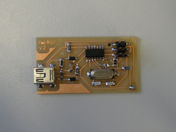

 Picture Source: David Mellis' FabISP
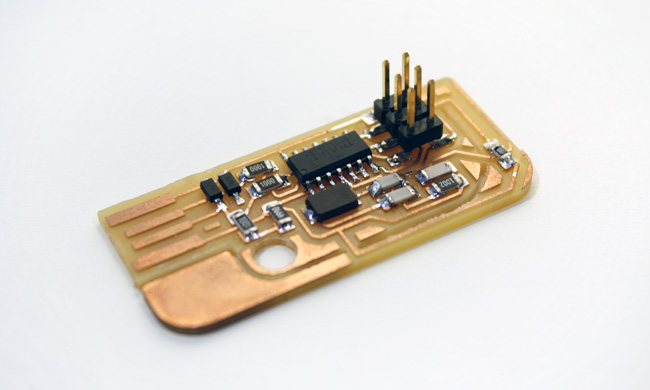
Picture Source: Andy's FabISP
Picture Source: Valentin's FabISP
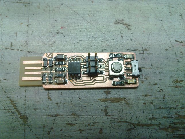
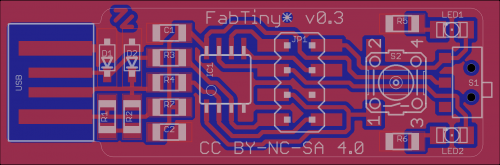
Picture Source: Zaerc's FabISP
Picture Source: David Mellis' FabISP
Picture Source: Andy's FabISP
Picture Source: Valentin's FabISP
Picture Source: Zaerc's FabISP
Following this excellent tutorial by Jean-Francois Duval, I set about fabricating my FabISP module:
MILLING

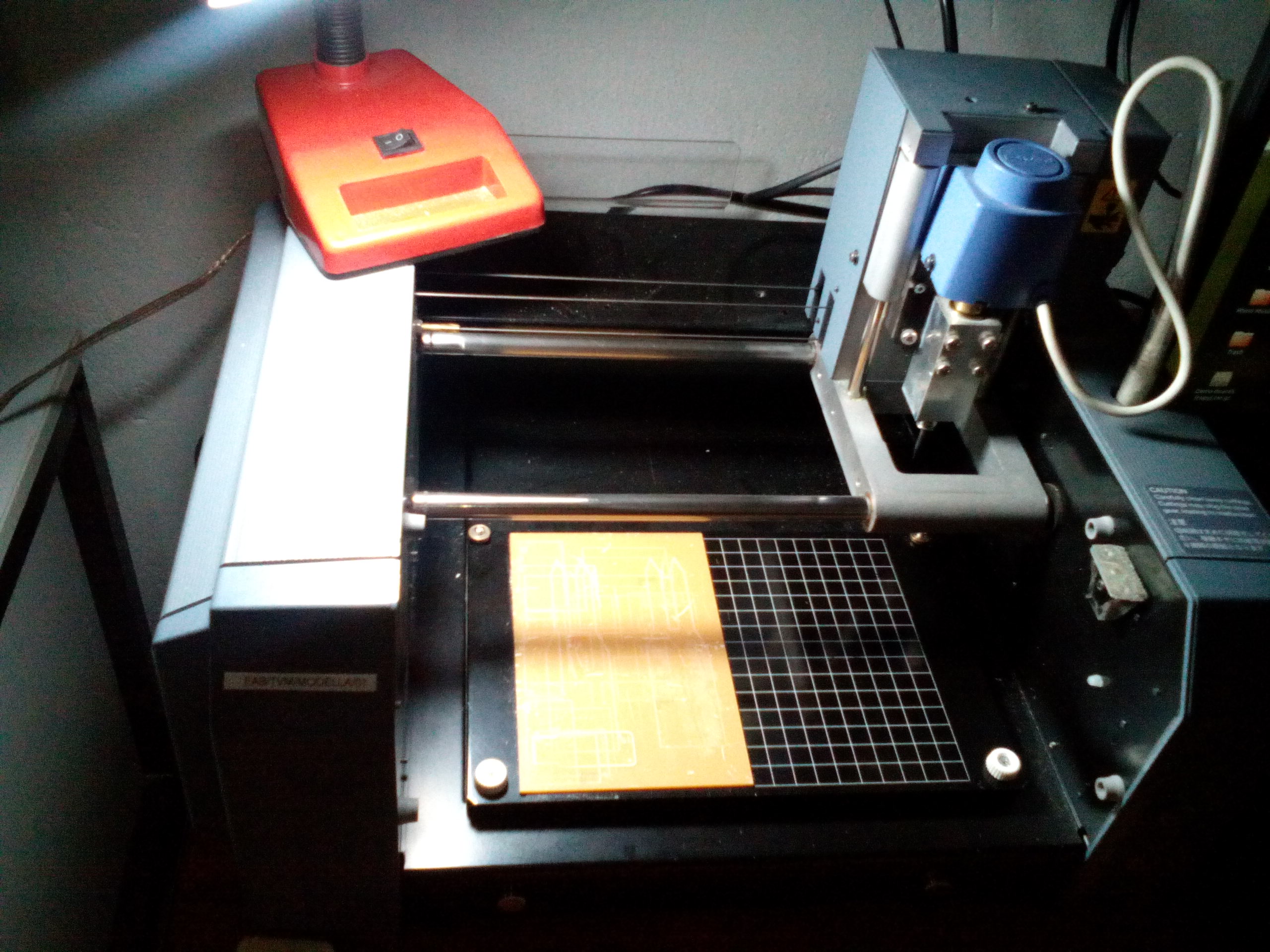
 Picture Source: Photo taken at Fab Lab Kerala
Picture Source: MDX-20 partnames
Picture Source: Photo taken at Fab Lab Kerala
Picture Source: MDX-20 partnames
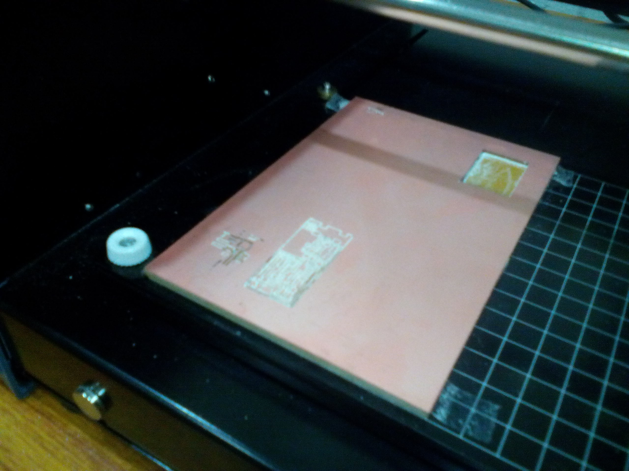
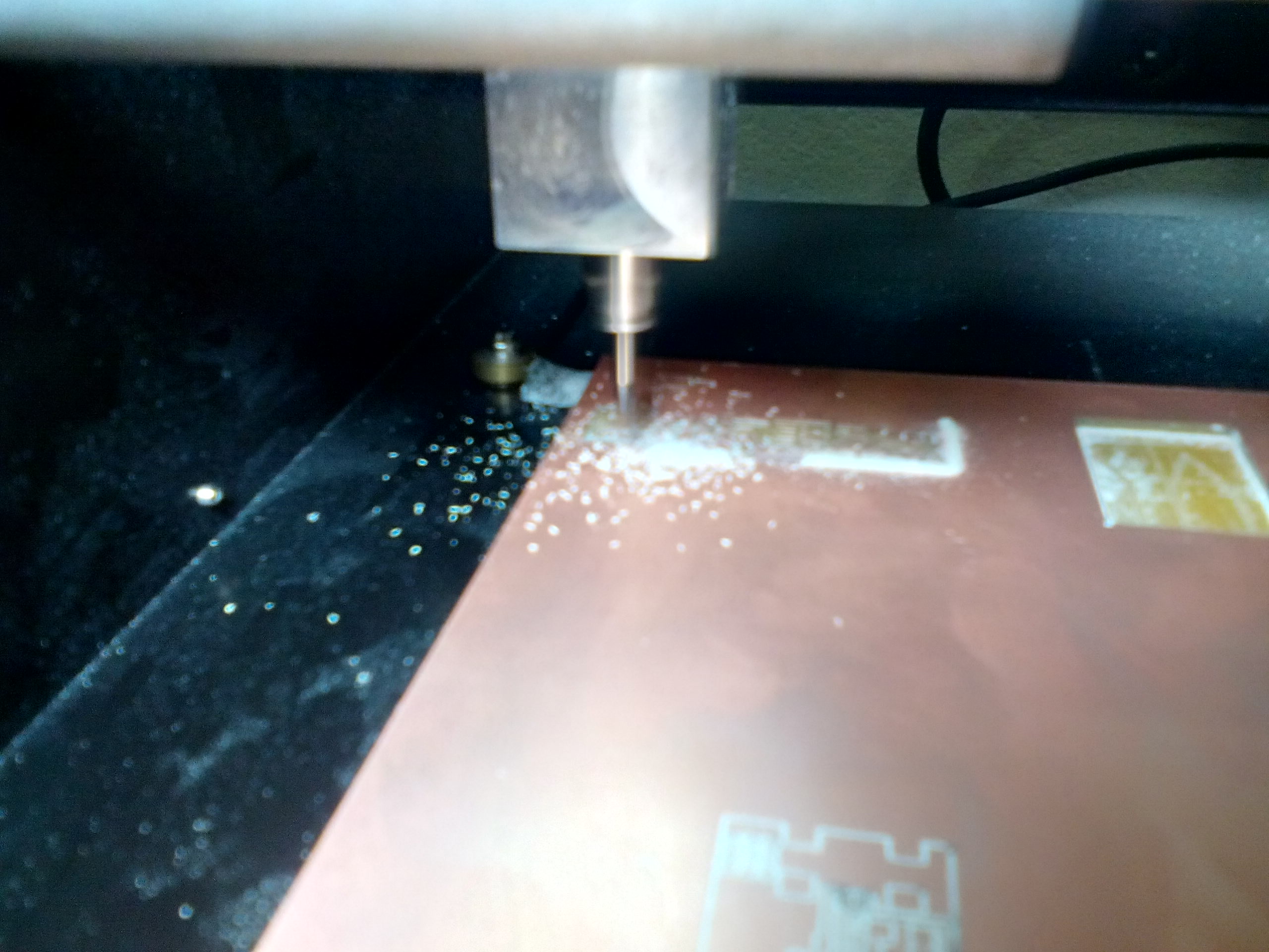
B. I then "prepped for machining" using the Modela MDX-20:
- I proceeded to follow the correct safety precautions when preparing my FR1 copper-clad PCB substrate, by first ensuring I had a "sacrificial material" (i.e. an unused FR1 board, but turned upside down) affixed on the
Work Plate of the Modela Mill.
- I used double-sided adhesive tape, being careful to not trap any air bubbles, on the underside surface of the FR1 copper clad board I was intending to mill on --> and affixed it onto the sacrifical layer, lining the edges such that both boards were superimposed on each other

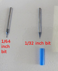
- My next step was to verify which
End Mill would be used to machine which part of the FabISP: The 1/64 inch End Mill for the first part - Circuit Traces; followed by the 1/32 inch End Mill for the Circuit Outline
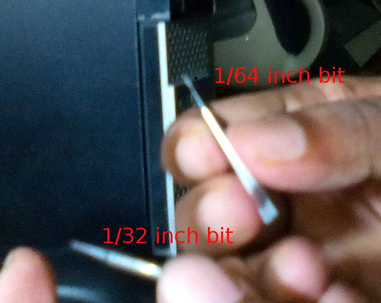
- Mounting the
1/64 inch End Mill on the Carriage of the Modela, I used the accompanying allen key to adjust the Carriage Nuts which would ensure the end mill/mill bit would stay in place in the Carriage; with guidance from my classmates on distance (up) the Carriage
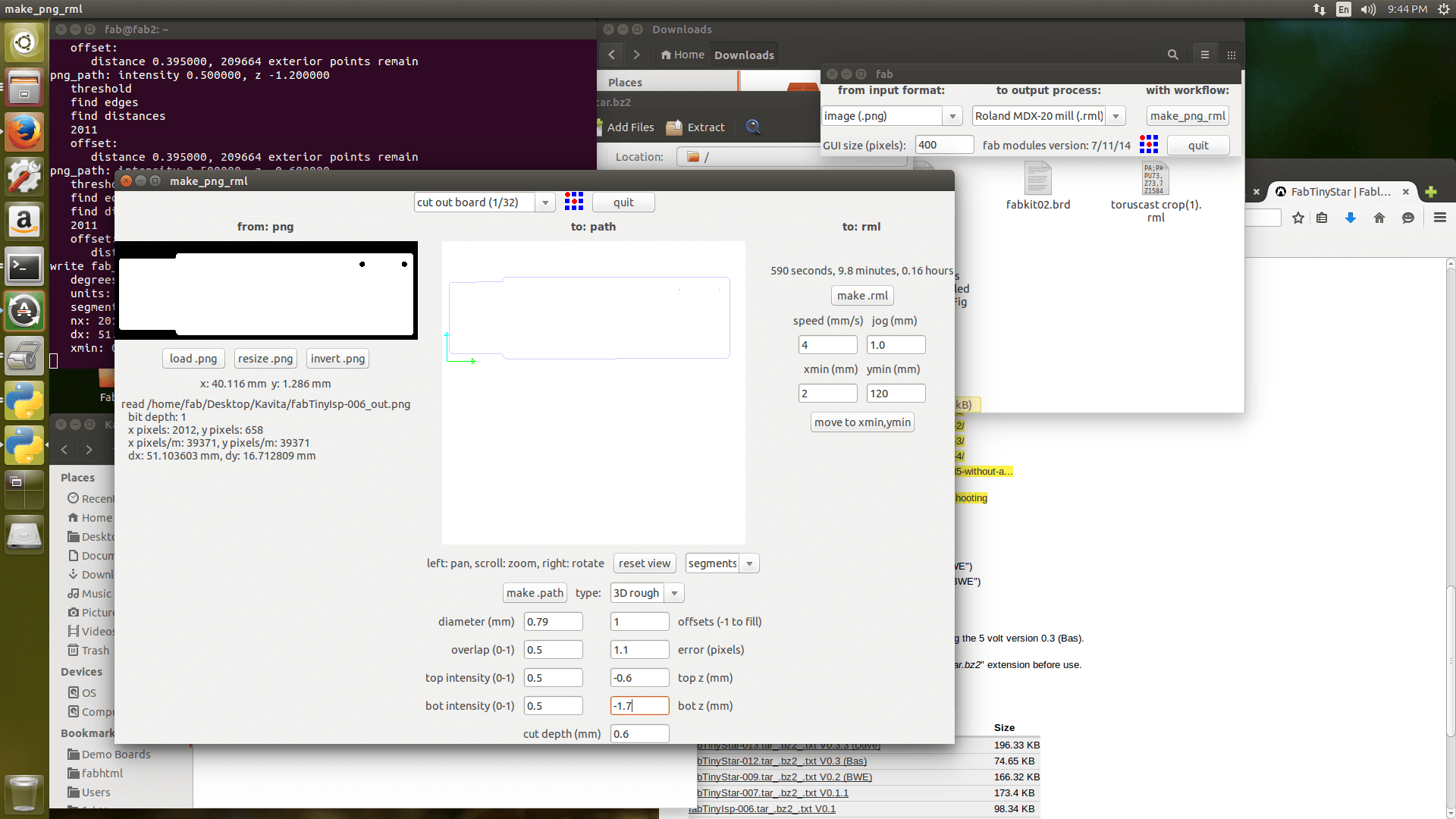
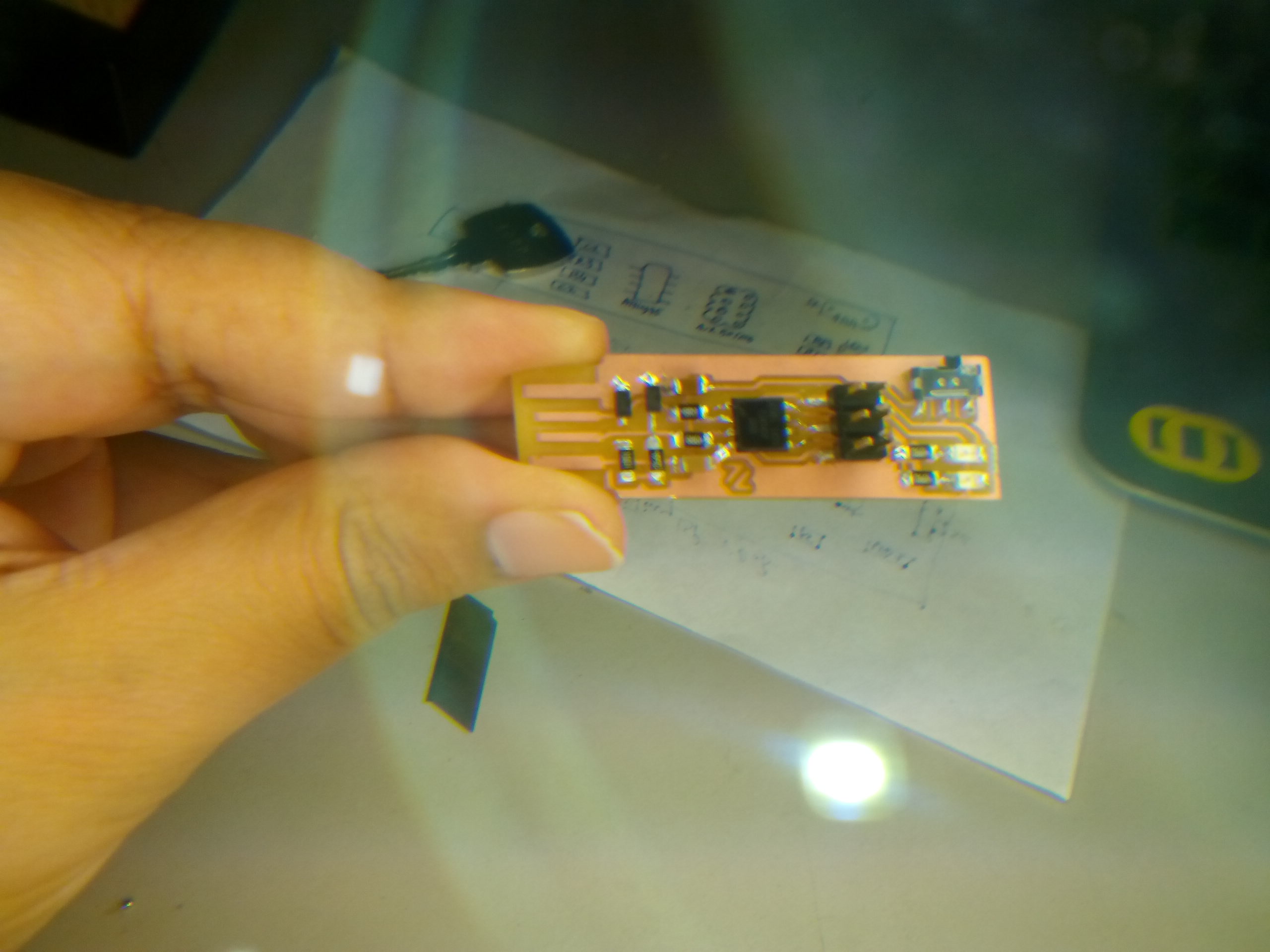
C. After ensuring the End Mill was secure and at the right distance from the copper-clad board; I executed Fab Modules which brought up the dialog window. I loaded the .png of the FabISP (Zaerc's fabTinyISP) I had chosen to base my design on:
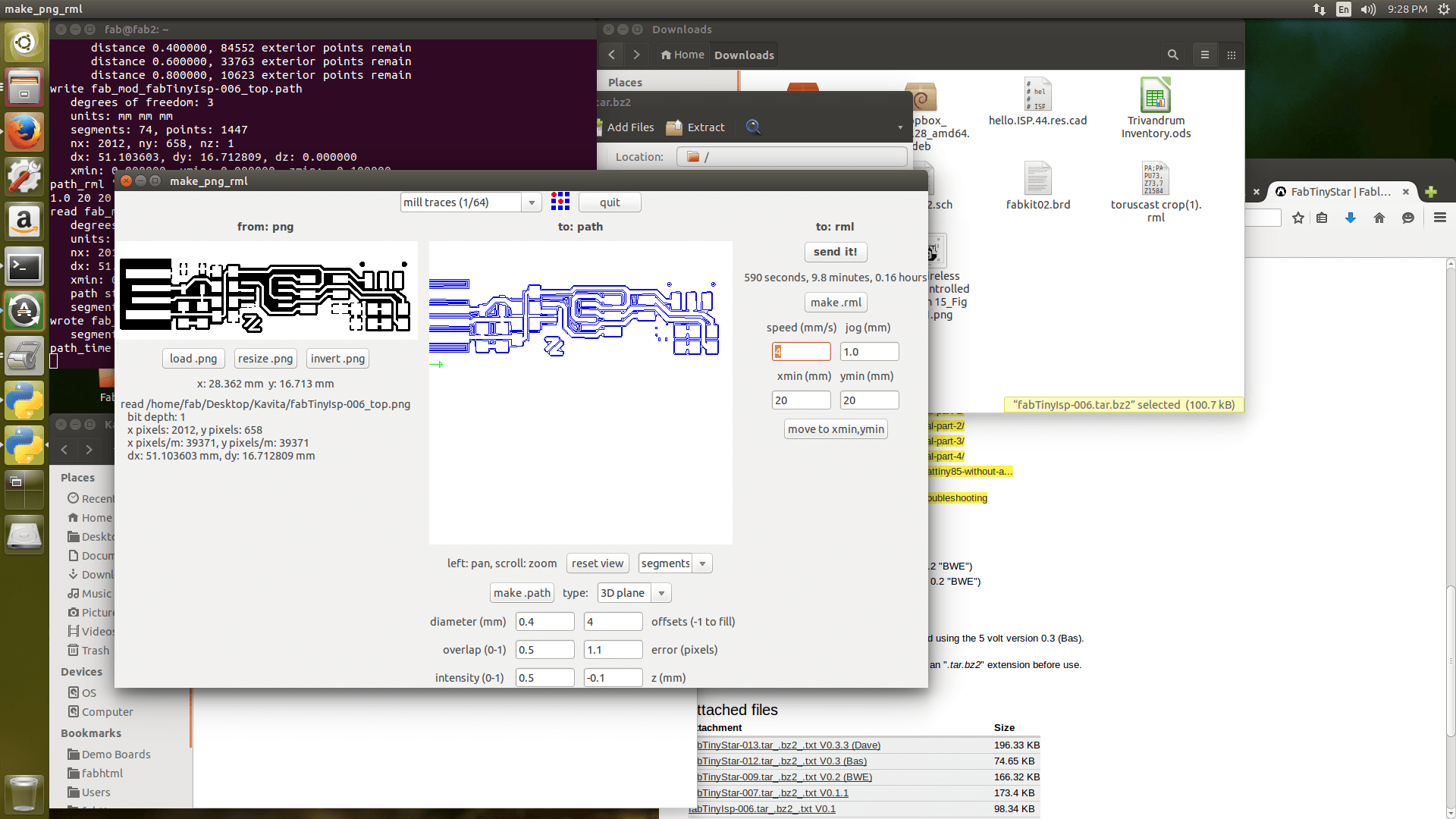
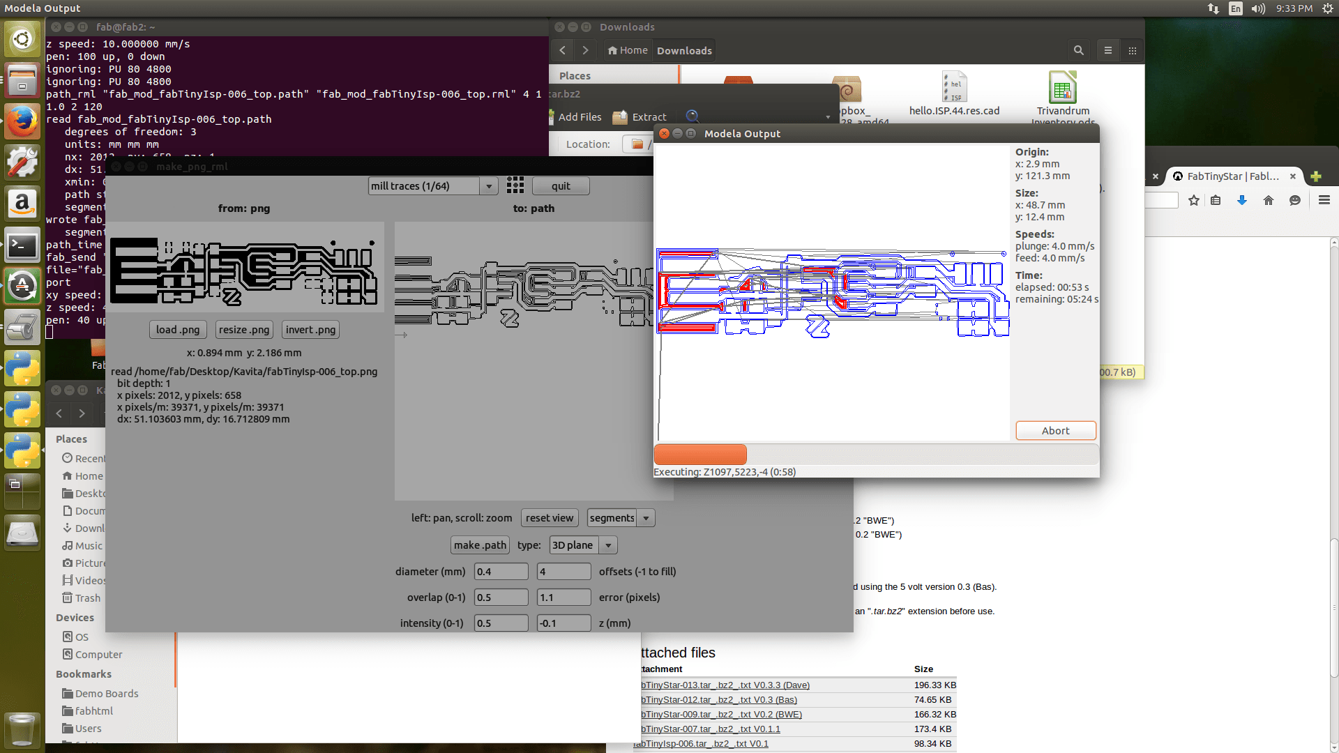
The inner traces of the FabISP were milled first on the Modela:


Followed by the outline cut, for which we replaced the 1/64" End Mill for the 1/32" End Mill:


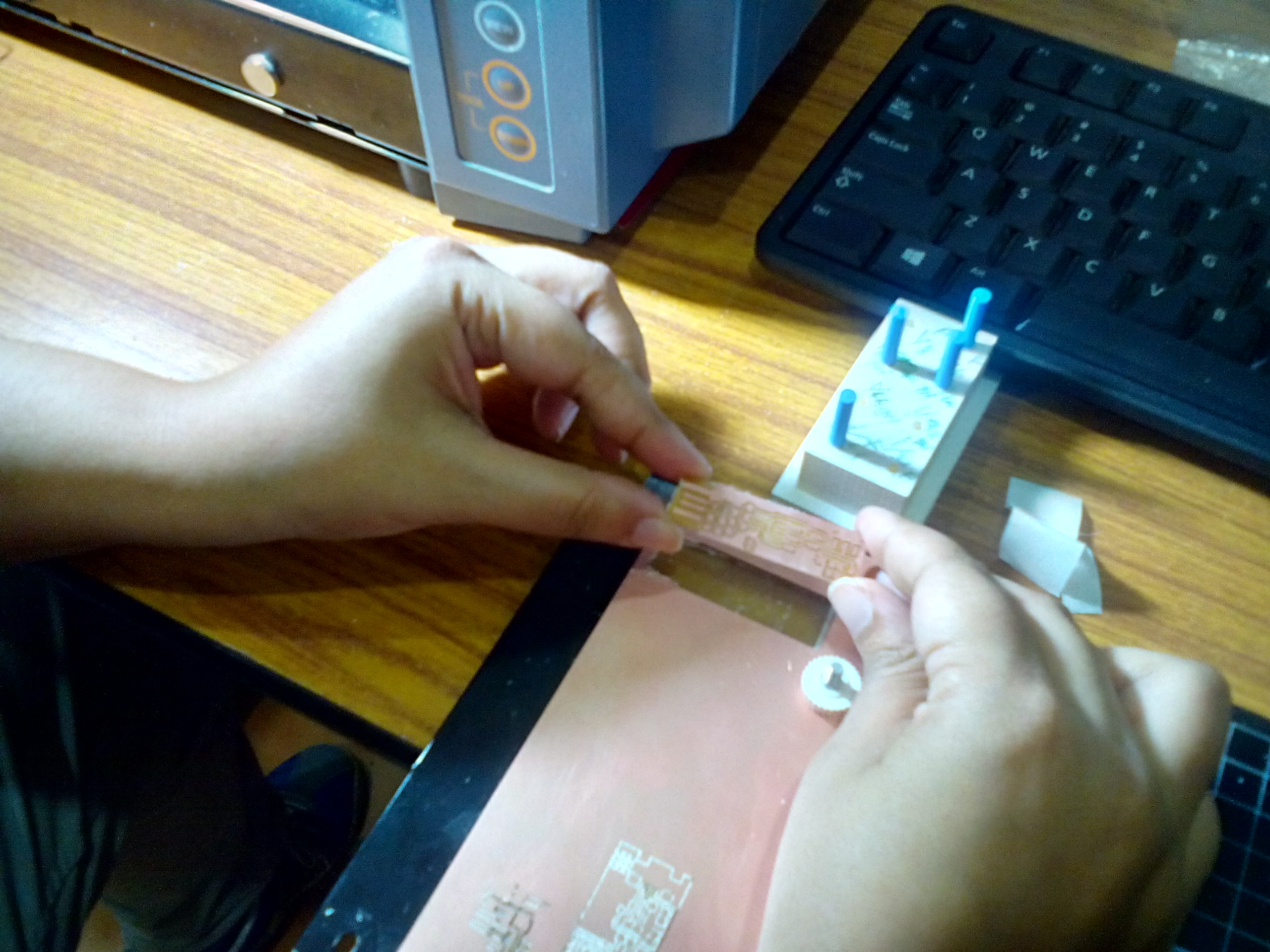
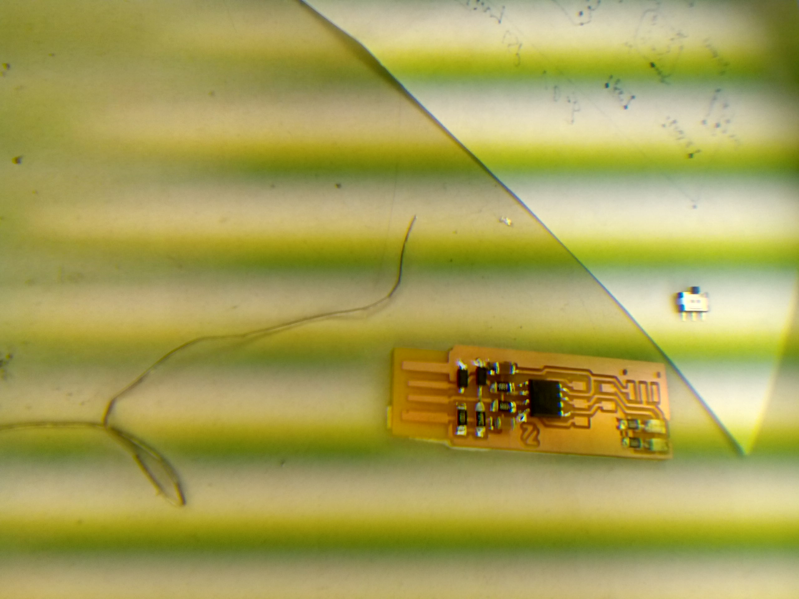
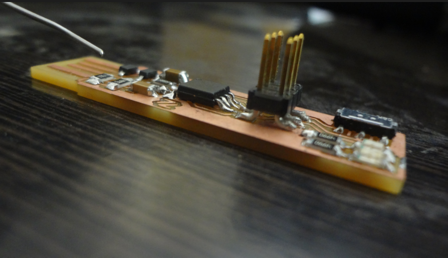
STUFFING

Since we were using SMD components it was impossible to simply "pick them up" one-by-one without having some kind of indication of what each component was just by looking at them, so I used a paper "organizer" to draw boxes around each of the components in the BOM as I retrieved them from the Electronics Component Storage in the Fab Lab:
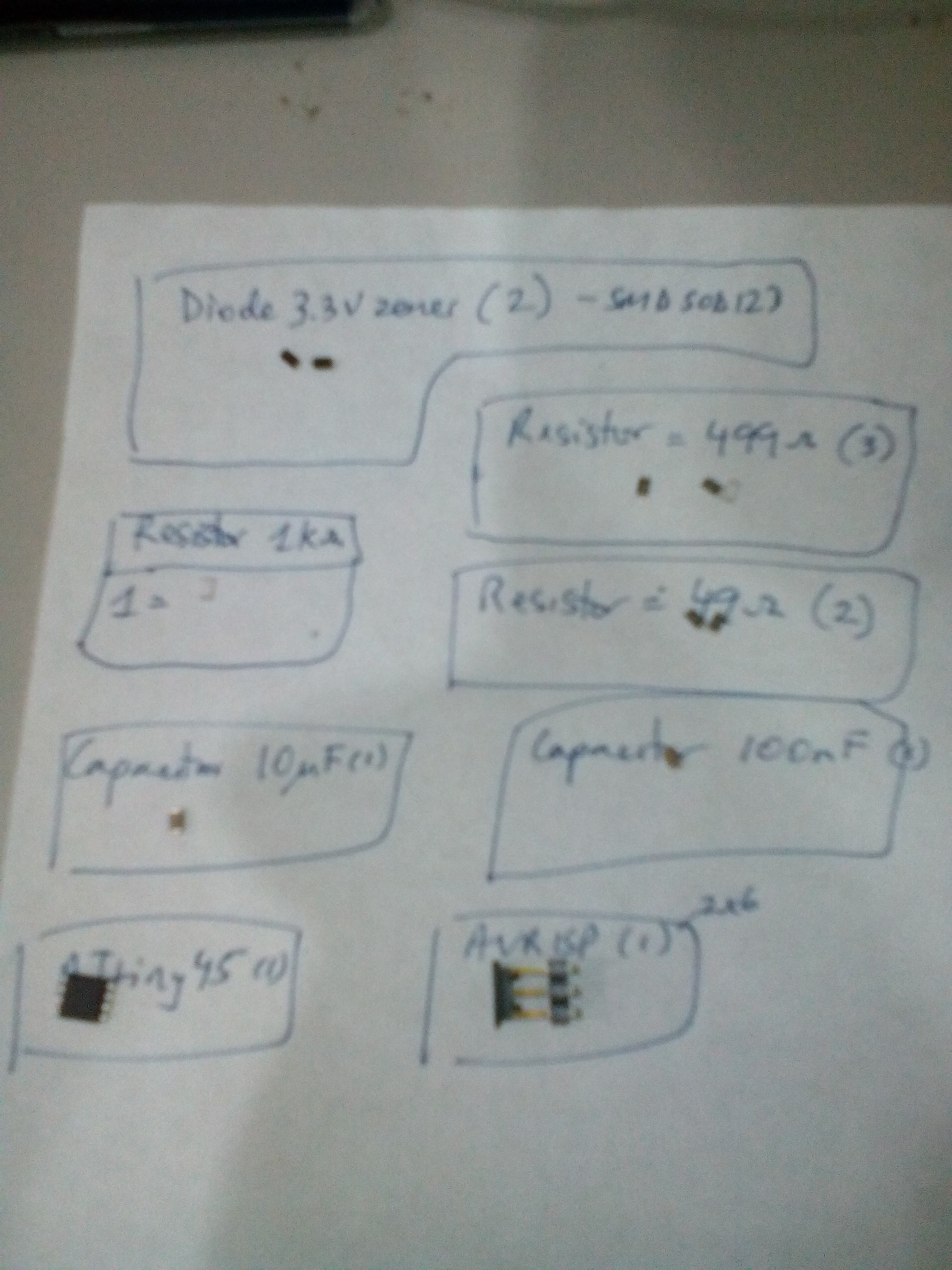 I followed these best practices when stuffing the board:
- I was careful to use the correct end of any components that needed to be biased in a certain way e.g. like the Zener Diodes and the LEDs
-
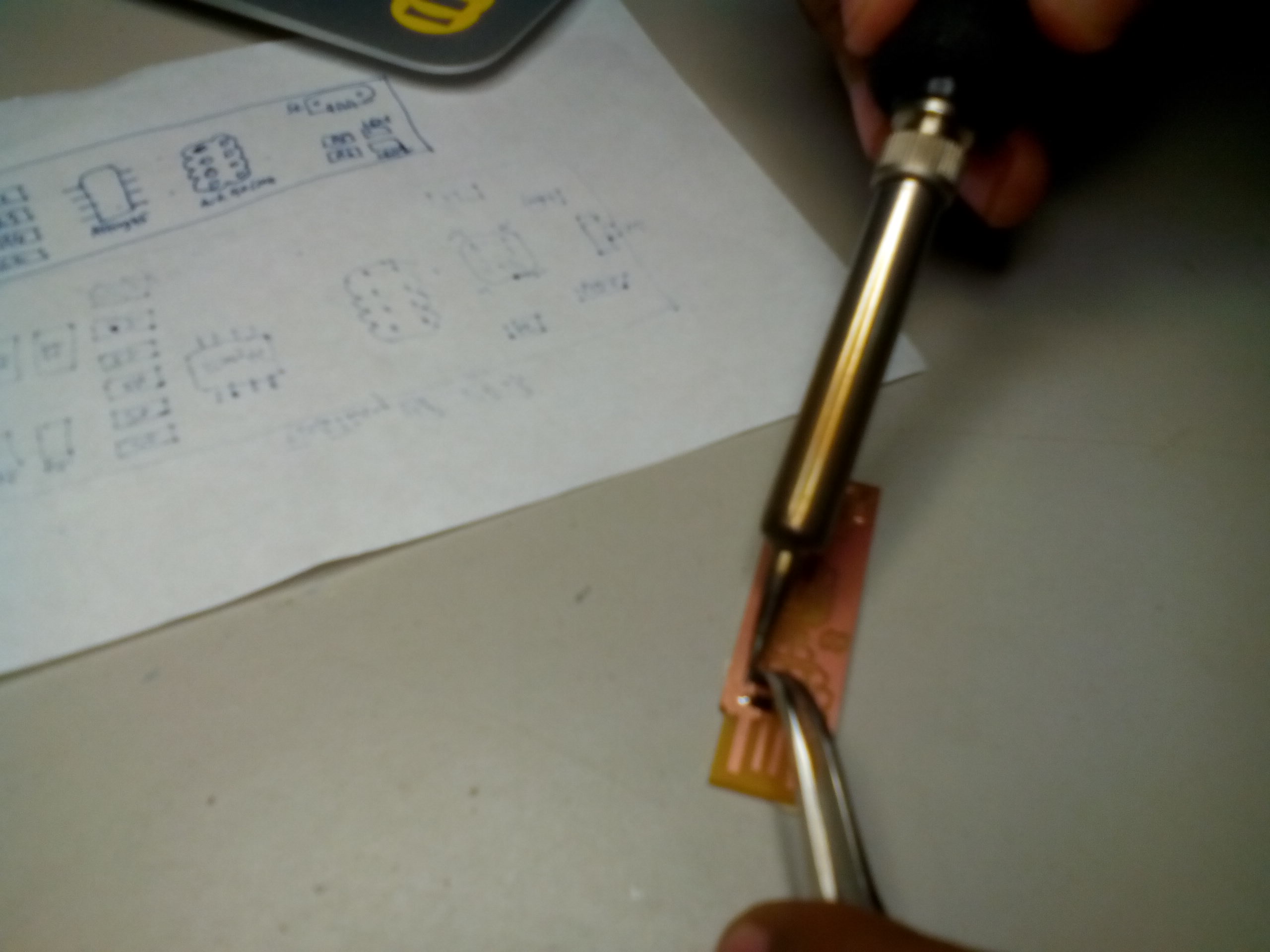
I used Solder Flux on the bare PCB board, before applying heated solder on each of the components and "gluing" them in place
- I soldered all the inner components first, which I'd new would be difficult to solder once other outer components had been soldered
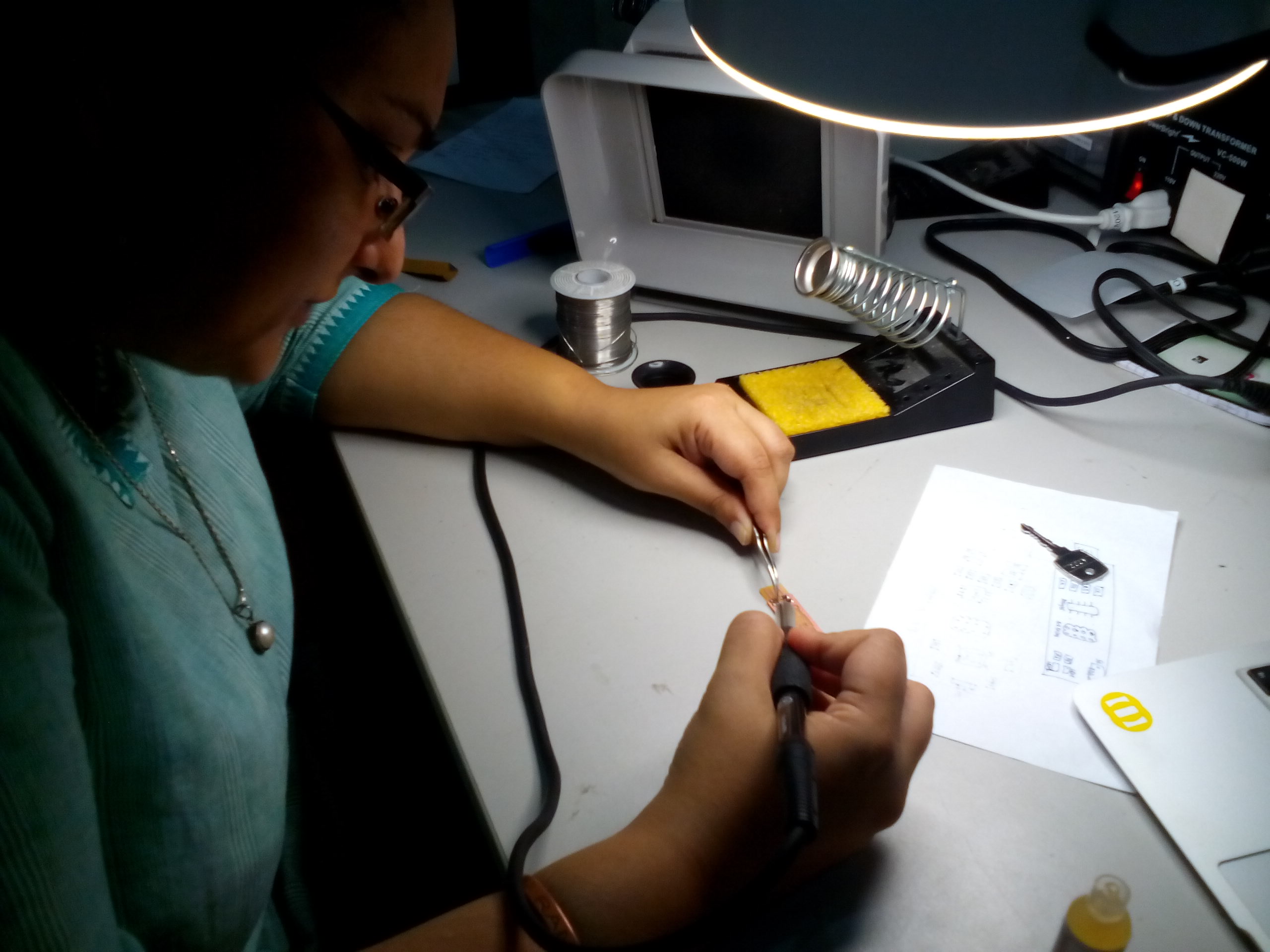
ASSEMBLY + PROGRAMMING
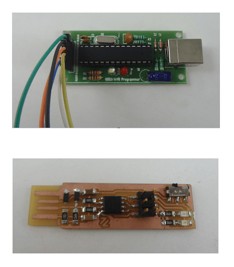
I managed to finally understand how to write the bootloader onto my new FabISP :) I used the Arduino IDE (version 1.6.4) selecting "ATTiny45" as the Board and "USBasp" as the programmer, since I used an 8051 AVR Programmer based on the USBasp design (http://www.fischl.de/usbasp/) to install the AVR bootloader to my newly stuffed FabISP (based on Zaerc's v0.1 FABtinyUSB). Here is the sequence of steps I followed in order to complete this task:
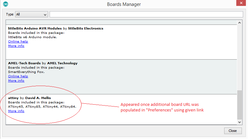
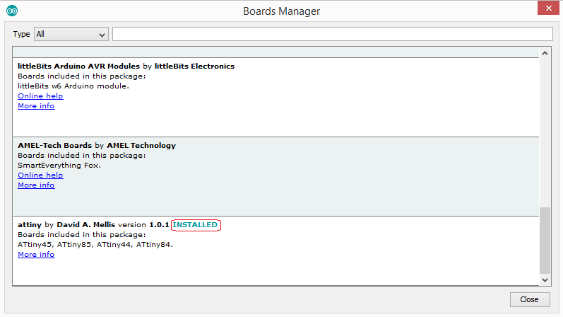
- Initially, when one loads the Arduino IDE, under the "Tools" menu, the default selection of Board is usually predefined as "Arduino/Genuino UNO" or the last saved board listing. Boards using the ATTiny chip are not listed by default within the selection menu. In order to select the appropriate ATTiny45 board I had to go to "Boards Manager" sub-menu and see what options I could use:

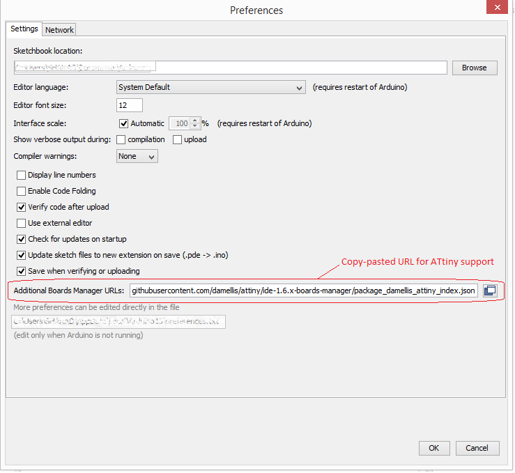
- According to the Tutorial listed at Hi Low Tech dot org's webpage I followed the instructions which enabled me to install ATtiny support using the built-in Arduino IDE boards manager (via entering the URL for ATtiny within Preferences):
-
Going back to the "Tools" menu, an option to select "ATtiny" became visible, I selected that option and installed the requisite ATtiny package:
- The next step was to select the correct board parameters, so as soon as I could choose "ATtiny" as the board, I selected the Processor as "ATtiny45" (which was the chip used in Zaerc FabISP v1.0 design); set the Clock speed to "8 MHz (internal)" and selected the Programmer as "USBasp" corresponding to the AVR programmer I was going to use on my new FabISP:
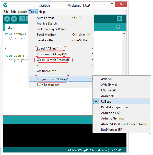
- Once board and programmer settings were established, I had to burn the bootloader onto the FabISP v1.0 via the USBasp programmer, by selecting "Tools --> Burn Bootloader"
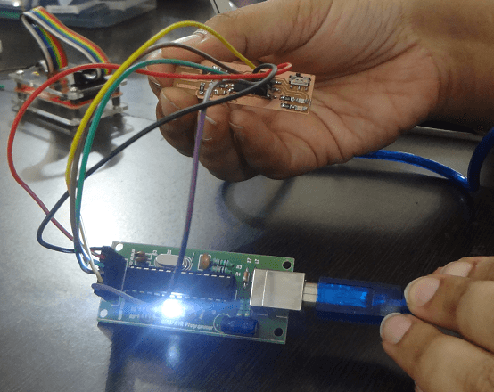
- It worked! The ATtiny45 chip had been detected and programmed! The led glowed red to indicate as such

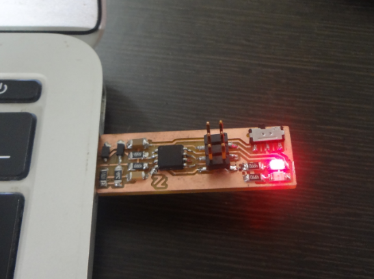
My next step was to ensure that I could flash the firmware as provided in Zaerc's "vusbtiny.hex" file. For this, I had to make sure the Fuse Bits on the newly bootloaded ISP had been set correctly. I used a friend's laptop to independently determine this:

- To further test the FabISP, I connected an Arduino via the 6-pin ICSP ribbon cable and ran the blink program.

Note: Since I used the standard "Blink" program that is listed within the Arduino IDE examples, I did not feel the need to attach the file here on my page due to space constraints within our FabLab's group's repository.
Extra
For this assignment I had milled and stuffed Zaerc's original FabISP board v0.1 (which was previously hosted at http://fablab.waag.org/project/fabtinystar/documentation/8259 but was suddenly discontinued). As a safety precaution, while updates were being made to Zaerc's page, I also happened to mill his latest FabISP v0.3 board as depicted on http://fabacademy.org/archives/2015/doc/FabTinyIsp/index.html

I wanted to further my understanding of AVR programming and what it meant to write a bootloader to a new in-circuit serial programmer, so I used a different device called the BUS Pirate - an open source universal bus interface that talks to most chips from a PC serial terminal. I am still working on this and will update results as and when my final project information is complete!
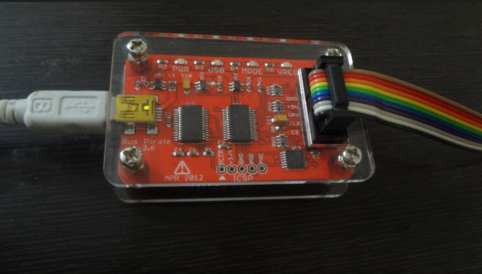
Bus Pirate is an Open Source Hardware device manufactured by [Dangerous Prototypes]
Next Steps: To use the FabISP(s) to program future PCBs I fabricate during Fab Academy :)
Go back HOME