Silk, top layer,bottom layer, ratsnest, routing, pads, vias, smd,through-hole, netlist, gerber,footprint, mils.
We try to redraw the [echo hello-world board] (http://academy.cba.mit.edu/classes/embedded_programming/index.html#echo), add new components to it. I will try to add two leds and one push button.
By this I am trying to find out What is better?,
An LED connected to GND(ground) and control signal of +5V given by uc(microcontroller) or led connected to VCC(+5v) that is given ground signal given by uc? I have connected the LEDs in both configurations.
I went through the following video tutorials to get started in eagle.
https://www.youtube.com/watch?v=1AXwjZoyNno
https://www.youtube.com/watch?v=CCTs0mNXY24
Workflow
The workflow for most electronics design software is similar.


a sample auto routed circuit path.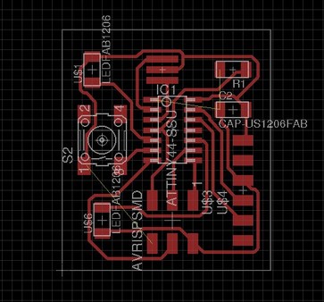
Sample png (do not use for production)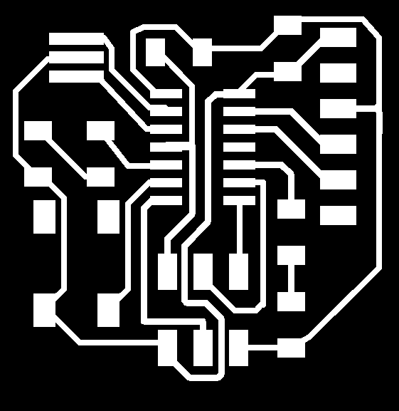
I tried to use Kicad. and found that it is not as intuitive and appealing as eagle.
I added fab library of components(Preference->library->add) from http://fabacademy.org/archives/2015/eu/students/haldin.anders/assets/week6/kicad_fab_librarys.tar.gz
The components locally available in from the software didnt show any issues in zoomin.
The eschema didnt respond to save option too due components being larger than the page layout.
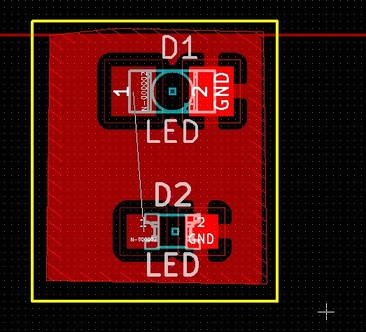
I tried a simple circuit of lighting an LED using the KICAD. The work flow is similar to eagle except that there is an extra step where you have to select the footprints of the components chosen.
Draw Schematic.
Annotate-This step is necessary before you generate net list.
Generate Netlist. I dont know what netlist is but this must the list of all the components used and the links between them that used to identify these components when assigning footprint in cvPCb and generating ratsnest in pcb layout creating part.
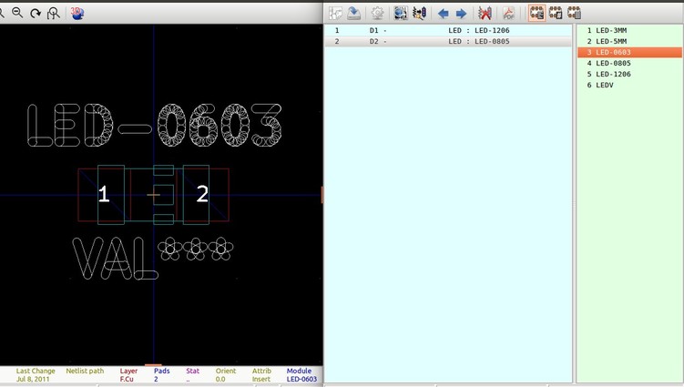
cvPcb -This is the step where you associate the components with the footprints. Open the netlist generated select each components and choose what kind of footprints you need for them.Make sure you enable preview. For some components you have browse through a very long list and figure out the thing you want, there is no option of user defined searching, I cant search smd or resonator and the names they use dont make very logical sense to a beginner, someone who knows how the sizes of the components are defined can use it better. This way it is not that friendly to beginners who don't know how to choose and what alternative you can choose.
Errors.
Graphic not authorised on copper layers
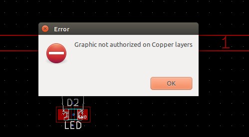
You have to select a non copper based layer. In the layer list box on the right you
will be able to see what are copper based layer. They are usually have cu suffix.
You wont be able to draw any other feature other than routings in a cu layer.
Auto-Routing
In order to make auto router work.
https://en.wikibooks.org/wiki/Kicad/Autorouter
I got an Error while building project in netbeans when I tried the instructions given in the link.
For now moving on and trying other softwares.
Impressions
Not intuitive, some things are out of reach from beginners understanding. It can be a good tool if you want to create everything from scratch like, components and their footprints etc.
Its an online pcb designing tool and you can visit https://123d.circuits.io/ to use it. You should have an autodesk account to start creating your deisgns. I chose to watch the intro video before starting with it. You will be given the option to watch a video when beginning.
Impressions
Creating schematic is very easy and you just have to click at the pads you want to connect
and the connection is drawn with meaningful bends paths. This makes it look neat at the cost of being slightly confusing as some
of the lines overlap. You might find it difficult to trace it visually. It allows many cool features like collaborative development options, sharing etc.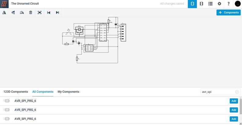
While adding components, a quick preview would have been useful,but not to worry
these are just a symbolic representation so you dont have to worry a lot about the
footprints right away.You can choose them later. If you click on the component it will take you to a detail page in which you can see all the kind of footprints you can choose for them.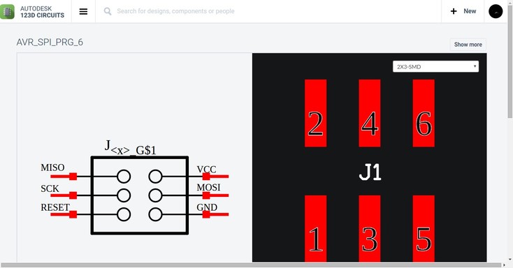
The ratsnest is instantaneously generated that allows you to make better judgement on placing components.
There is option to rotate a component in 45 degrees too.
There is no auto routing option. It has an extensive library of components and it was a joy to work on it. By far the most easiest to use and user friendly and beginners friendly. It will output only in Gerber format.I tried gerber import option of eagle 7.5, to see if it can be further worked on in eagle but it didnt work.
Download (unrouted circuit) gerber file
There are No shortcut to rotate compoents which i missed the most, no keyboard shortcuts. Very click and drag oriented. It has a great component library but not as extensive as 123d circuits. I couldnt find attiny 44 and ftdi smd, avr isp 6 pin smd() instead used avr isp offset). The components are easily searchable. It has search option from different vendors, spark fun, arduino, seed etc

You can choose the values and footprints for the components too.

It has breadboard view and code view in addition to schematic and pcb views. All these are connected with each other. And what the code view means is that it run some programs as well. But I cant comment on what kind of codes will it run and how it works. BUt it seems like a great solution.
Creating schematics is similar to point and click method used in 123d circuits but here it allows you to form the shape of the connections.
In the following pic I have not bothered to form good wiring shapes. for the schematic.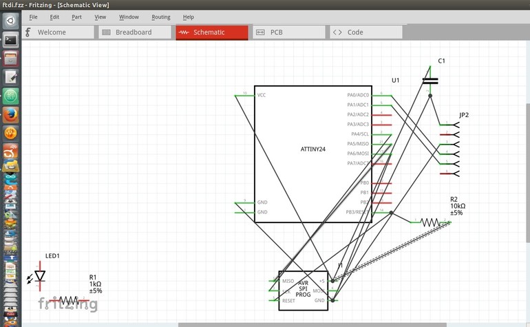
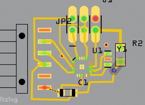
It has clumsy handling in pcb view. The routings created looked messed up. It gives us great freedom to route but it wont look great and the handling could be improved.
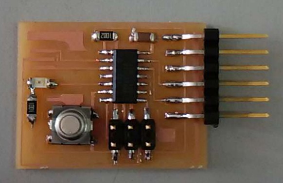
I have undergone pre-academy workshop with Franciso Sanchez and Luciano Betoldi during which time I used Kokopelli and made desined and made the hello ftdi with a button and led added. I will continue to use that board. Click here to go the page.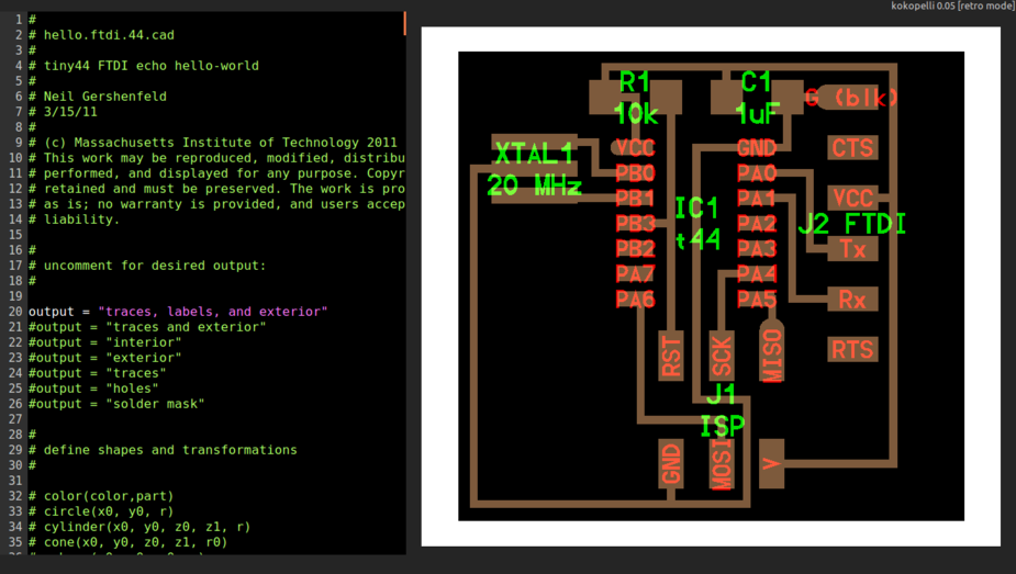
Circuitlab(https://www.circuitlab.com/editor) is a very good and beginner friendly online circuit simulation tool. I dont know what DC Bias, dc sweep, transient and ac analysis mean but it allows you to do these things. I understand that there is an input signal for a circuit(AC,DC, current or voltage) and you expect an output from it (filtering, square wave, amplification etc) and that I hope to understand from the graphs generated from the simulations. The only drawback is that it is trial version and you have only few hours to practice on it before you would need to buy a license for it. The introduction video is enough to get you started on it. Unfortunately I left my browser on for too long without attending to the webpage and my trial hours got exhausted before I could check the simulation and do other changes.
I tried to replicate the circuit of a transistor being used as a switch in the simulator but found that this would be meaningless for analysis unless I introduce a switch or better use a square wave voltage source in the signal side of the circuit and observe the output side voltage. But before I could do all these I ran out of time.

What like about Cicuit lab is that it is very beginner friendly, it has a number of example circuits that users can play with and learn using it. It also offers a 90 day trial option afer you have exhausted your one day trial.

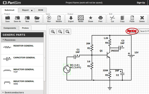
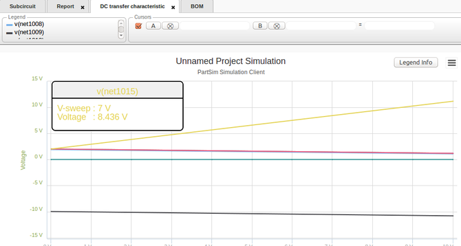
PartSim (http://www.partsim.com/simulator#) is another online simulator. It doesnt have time restrictions and also allows you directly add components from digikey directly. It can do DC Bias, dc sweep, transient and ac analysis. Here I tried to simualate transistor as an amplifier
I coundn't understand much from the graphs generated here. It not a type of representation I am used to nor did I understand what was v sweep.
I used the files generated by kokopelli for fabrication. Used fabmodules html version and Modela mdx 20 to make the board.
The final stuffed board.
(Resonator missing, forgot to stuff it in eagerness)