
This week we started with electronics production. The goal was to fabricate a pcb from an already existing design of fabISP using Roland modela and fab modules..
Downloaded files from
http://fab.cba.mit.edu/content/projects/fabisp/fabisp.png
http://fab.cba.mit.edu/content/projects/fabisp/fabispdim.png
Mounting PCB.
We need to mount a sacrificial layer on the modela bed first. On top of this layer we place the layer we want to mill. It is recommended that the sacrificial layer is stuck such that the plastic side is facing up. This plastic layer is much easier to be milled if the tool plunges into it. Make sure most of the area is covered by double sided tape. We used the white double sided tape instead of the transparent scotch tape. There are some advantages for using a white double sided tape. One is it has a larger area and it will be easier for us to cover the area. This makes sure that all areas of the pcb stuck to the base and are flat. Make sure there are no bubbles if you find some air bubbles remove them.
If the bubbles are at the edge it can be pushed to the edge, If it is in too much inside, puncture it and rub it flat using the shiny side of the double side tape paper.
While sticking the pcb to be milled use same guidlines as to secure the sacrificial layer namely, properly covering it with double sided tape and making sure it remains bubble free.
Here you can either use scotch tape on regular intervals of 10 to 15 mm across the pcb base or the white tape to secure the PCB for milling. We used the white double sided tape to secure the entire area. This wasnt perfect and after a while(two days) the corners loose adhesion and rise up, which caused some milling problems,hence I'd like to try with scotch tape once. The roland bed is reovable so a lot of these operations would be made easier by easy handling of the bed. Handle the bed carefully if it drops down of is subjected to large enough force that makes it bend it wont be able to produce good quality leveled surface anymore.
A nicely aligned and secured arrangement looks like the picture here.
Removing and securing the endmill.
Be careful removing or fixing the bits. Hold it in a way that it doesn't drop. 1/64 inch bit is very delicate and susceptible to breaking.
Handling png.
Sometimes you might need to Rotate png to place it on you board depending on the space available to be cut. You need to note that rotating using a normal image viewer will not preserve the size information. It mostly will look the same but would have scaled. We should resize it when this happens therefore, make sure to note the original size of the png image when it gets loaded in fabmodules. When you upload a rotated image use the old information to scale it down to the required size.
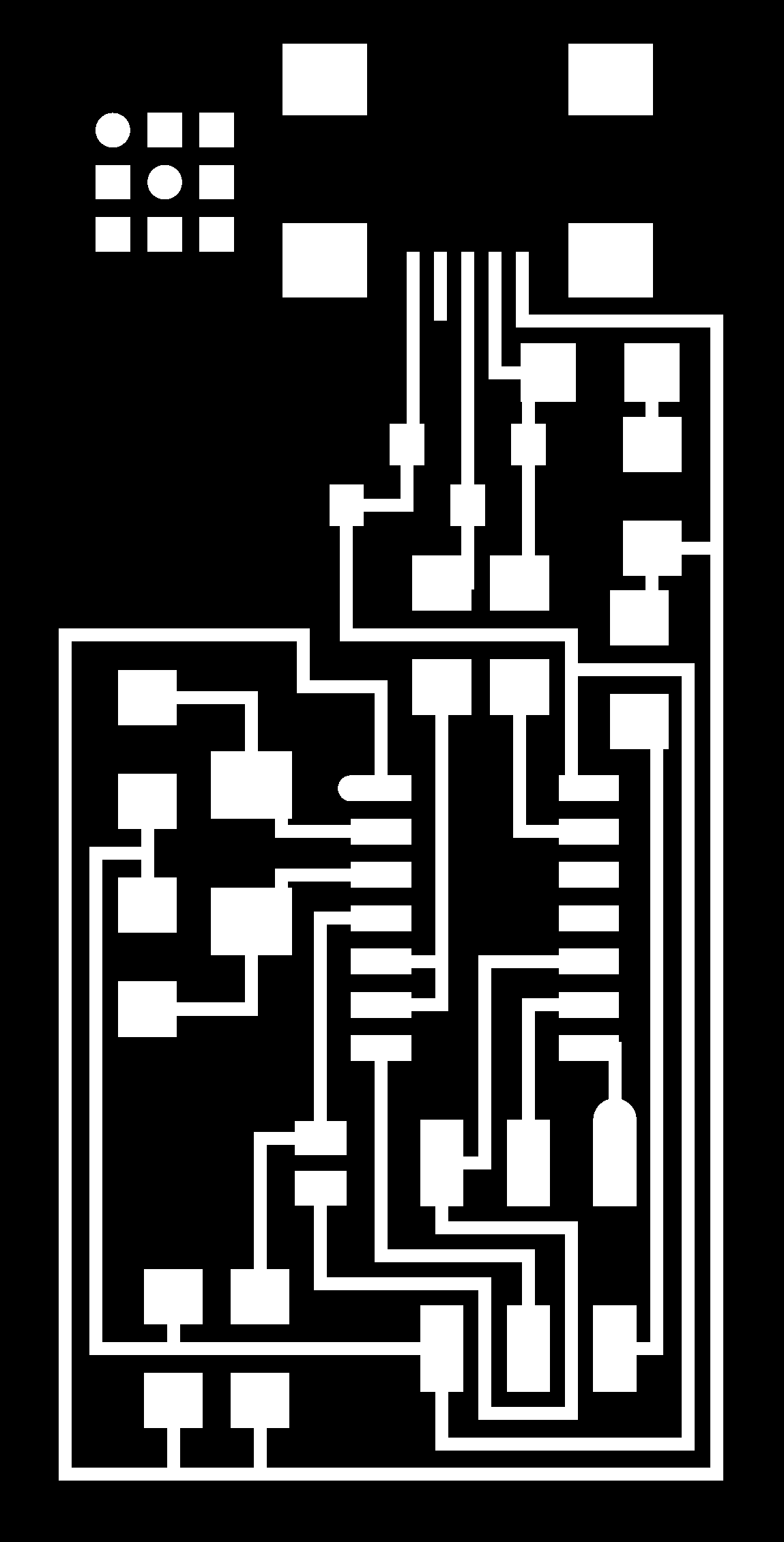
While making path in fab modules make note of the tool path generated. It shouldn't have any unexpected lines or moves. The move will be drawn as a line, a minor check on this before you start milling is recommended.
By default every trace is followed by 4 offsets cuts for isolation. This can be changed manually also by using the options given. If you want to remove all copper but the trace use -1 offset value, but with this approach the bit is used more and wear more per board so the number boards you can cut before the bit becomes useless is lesser.
Make path after every change. Mostly you can leave the machine parameter settings such as depth of cut or speed etc default. These will be different for different processes. We will be mostly using 1/64(inch) bit for milling traces and 1/32 bit for cutting the board.
If the pcb is completely flat it'll result in good clean traces. If not, in some places it'll not cut or cut too deep. if some areas are not cut, then u increase the depth of cut to 0.2mm or0.15, but only wen the job is finished with 0.1 trace. Directly doing 0.2 mm trace will mean more stress on the bit and more wear and less life or breakage.
Choose a good xmin ymin position. You need to measure the board area available and the size of board to be milled and choose a good location.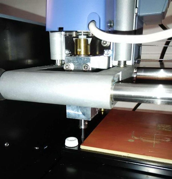
Vacuum debris, after job is done. Verify the job,
Problem: We have a broken trace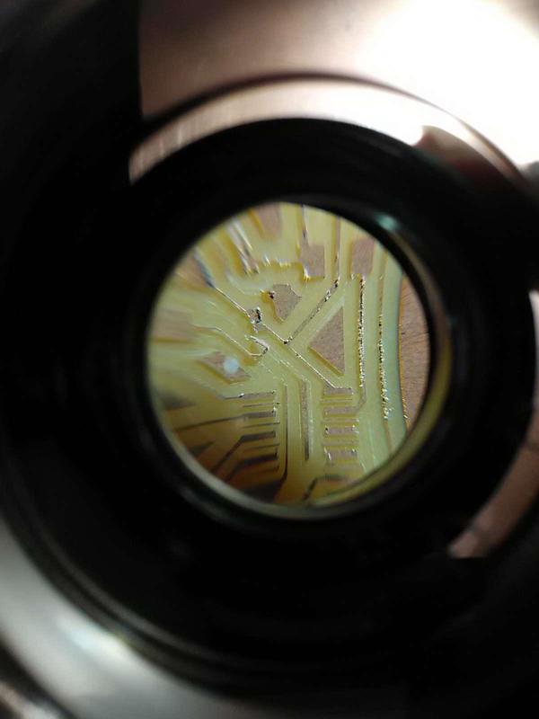
Cause: The traces are very thin, and the job now is useless. The traces shouldn't go out if you rub gently on the board or not be able to easily remove it.
So we download another version of the fabisp design(Neil version of fabisp) with thicker lines and try to mill again. The links for the design are below.
http://academy.cba.mit.edu/classes/embedded_programming/hello.ISP.44.components.png
http://academy.cba.mit.edu/classes/embedded_programming/hello.ISP.44.png
http://academy.cba.mit.edu/classes/embedded_programming/hello.ISP.44.traces.png
http://academy.cba.mit.edu/classes/embedded_programming/hello.ISP.44.interior.png
Board, dimension 22.98mm x45.2126mm
Zero position 2,55
Picking components for soldering. Go to the image where the components are mentioned.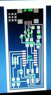
Note: this is a screenshot of a computer screen. The picture with components mentioned should be available from the links I quoted before.
General Precautions while handling smd electronics storage: While taking out components from the electronics drawers do not close it immediately let the box be open until you have put smd strip you have taken back into it. This is to avoid confusion when the smd is not labeled with it value or type. Capacitors can be tricky to handle because different value capacitor look almost the same. Make this a habit.
Prepare an arrangement like below. Write down material you need and pick the materials you need and arrange.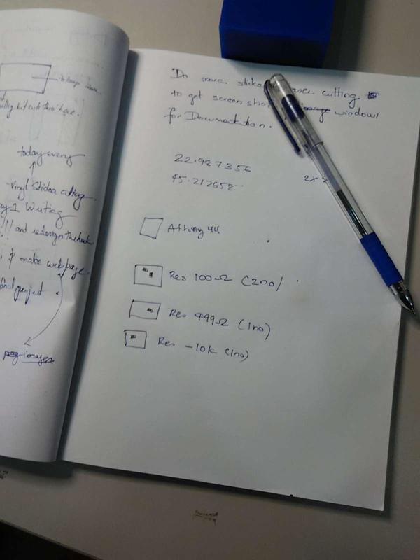
All traces look good by just inspecting with naked eye. The traces are thicker.
While removing the 1/64 exercise care Be holding it while removing.
Next we loaded the 1/32 bit and the outline image for milling.
Milled output.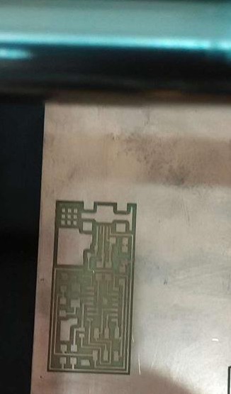
We need to pry the board out now. It would be stuck pretty firmly on double sided tape.
How it is done is you take thin ended object like the screw driver shown here. It should easily goes into the outline slot milled and move the board. Try to twist the screwdriver slowly and move the board slightly on all four corners.
Now try to pry the board out,
Pry from short side, the longer side bends doesn't bend. But below we try to pry from the longer side because the edge to the let side of the board of the base PCB broke and that gives us no fulcrum to lift the PCB up. Make sure you do not try to pry it from a sensitive area. Like an are where components or wires are passing through. This is another short coming of the white double sided tape-it holds too strong.
The board comes out with the double sided tape. The sticky double sided tape
Stick the board with double sided that comes out and place it on a table and start soldering.
Board is stuck making it easier to handle, it wont move while soldering.
Soldering order should go like more complex components to simple and middle of the board to border.
Fume extractor should be on.
Clean the soldering gun before you start the soldering operation. Opposite two diagonal corners of a component to all pins on each side one side at a time.
Difficult part is to place components, align them properly and soldering since the components are smd.
Alternate soldering technique.
Put component and use lot of solder and solder all pins together, then we can use copper braid to remove excess solder.
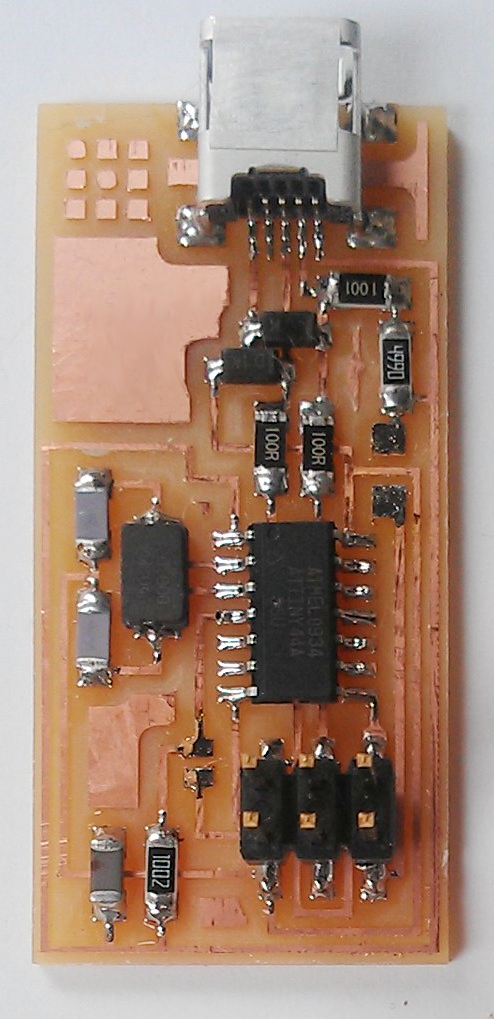
The final product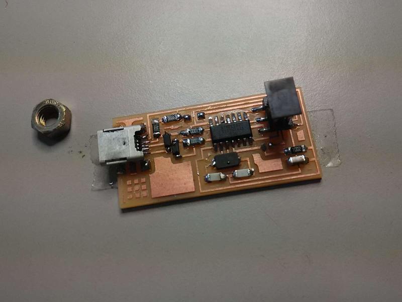
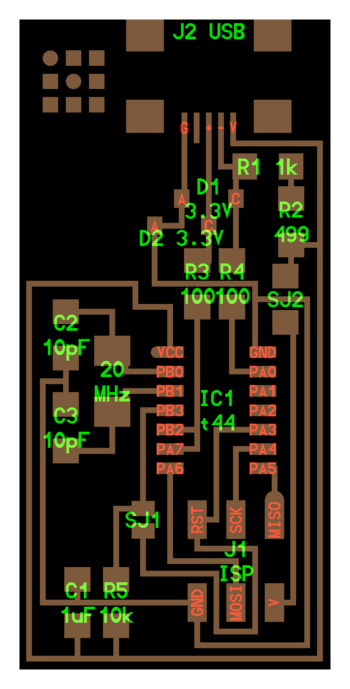
Note:You need to short SJ1 and add zero omh resistor or bridge for SJ2.Both are not shown in the figure above. You need to do this before programming.
Our FabISP is ready.
In ubuntu run the following
sudo apt-get install gcc-avr binutils-avr gdb-avr avr-libc avrdude
We need 6.1 version of avrdude
sudo add-apt-repository ppa:pmjdebruijn/avrdude-release
sudo apt-get update
sudo apt-get install avrdude
Add zero ohm resistor on SJ2 and short SJ1
Power the board through usb. It doesnt work with out this step. Connect to Atmel ICE, the notch of the pins pointing towards the inside of the board. Download the firmware and open the firmware folder in terminal type the following
make clean
make hex
Now go to the make file generate in folder and open it with text editor. Replace this line in the make file
#AVRDUDE = avrdude -c avrisp2 -P usb -p $(DEVICE) # edit this line for
to your programmer(Atmel ICE in our case)
AVRDUDE = avrdude -c atmelice_isp -P usb -p $(DEVICE)
Save the file and close
For the next lines the board had to be connected and live. Continue to enter these lines in folder opened in terminal.
make fuse
make program
Final step is desodler SJ1 jumper shorting. Now the board is ready to be used for programming other boards.