Electronics Design
For the past few years, I worked with bunch of EE engineers , electronics design is not a real stranger to me. Yet I had never do any layout job before by myself, so some bumps are expected.
At first I was thinking of using Altium to design tool, for that I knew it is powerful and preditable to me. Yet it only offers 15-day trial, I am not that sure if I could just uninstall-reinstall it to get access. So the safer option seems to be free version of Eagle PCB.
Eagle Tutorial on Youtube
Though it was filmed for old version Eagle, still highly recommend any Eagle beginner to go through these videos (at least EP1/EP2).
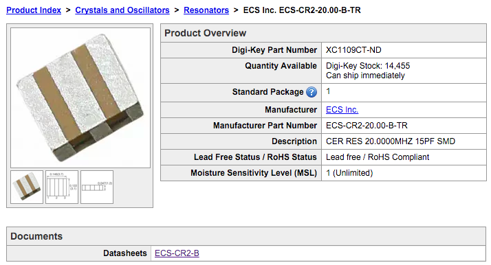
Since we don't have the 3-pin resonator in stock, I had to replace it with an equivalent.
ECS-CR2-B datasheet reveals that:
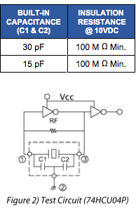
So I modified the design with one 20MHz crystal plus a pair of 15pF 1206 SMD capacitors. Not sure if this works, I will try to upload something to my board by the end of this week.
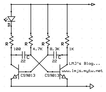
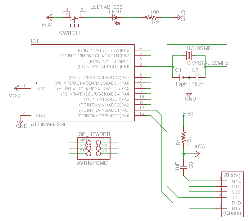
My original plan was to add an astable multivibrator to this week's board. But SMD BJT transistors is still on the way to our lab, so I decided to go back to the simplest design, with just one button and one LED.
Clean version (one button one LED)
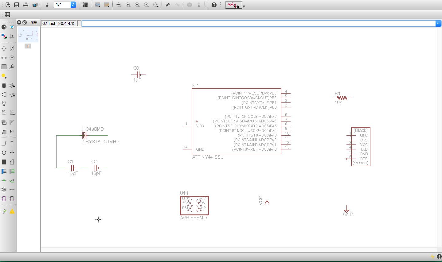
From component to schematics was not really a problem. Still, make sure you connect all the nets correctly, and double-check with the naming if you want to combine two or more nets together.
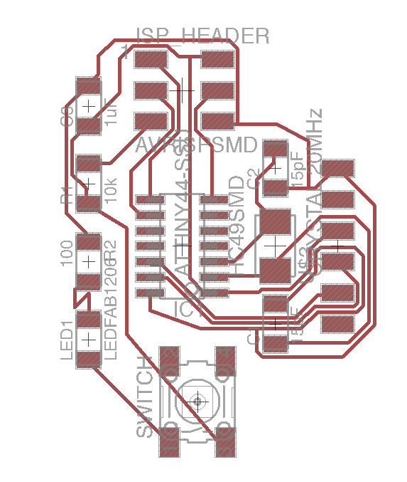
Cannot rely on the auto-routing at all, so I thought I should manually place all the traces. Won't be a great deal but need more hours on this one.
#Mar 12 Update
Finally get the layout done, with proper settings, the auto routing was not so bad at all. Yet I finalized the traces manually, for that it is still more convenient if you want to layout for desired shape at this scale.
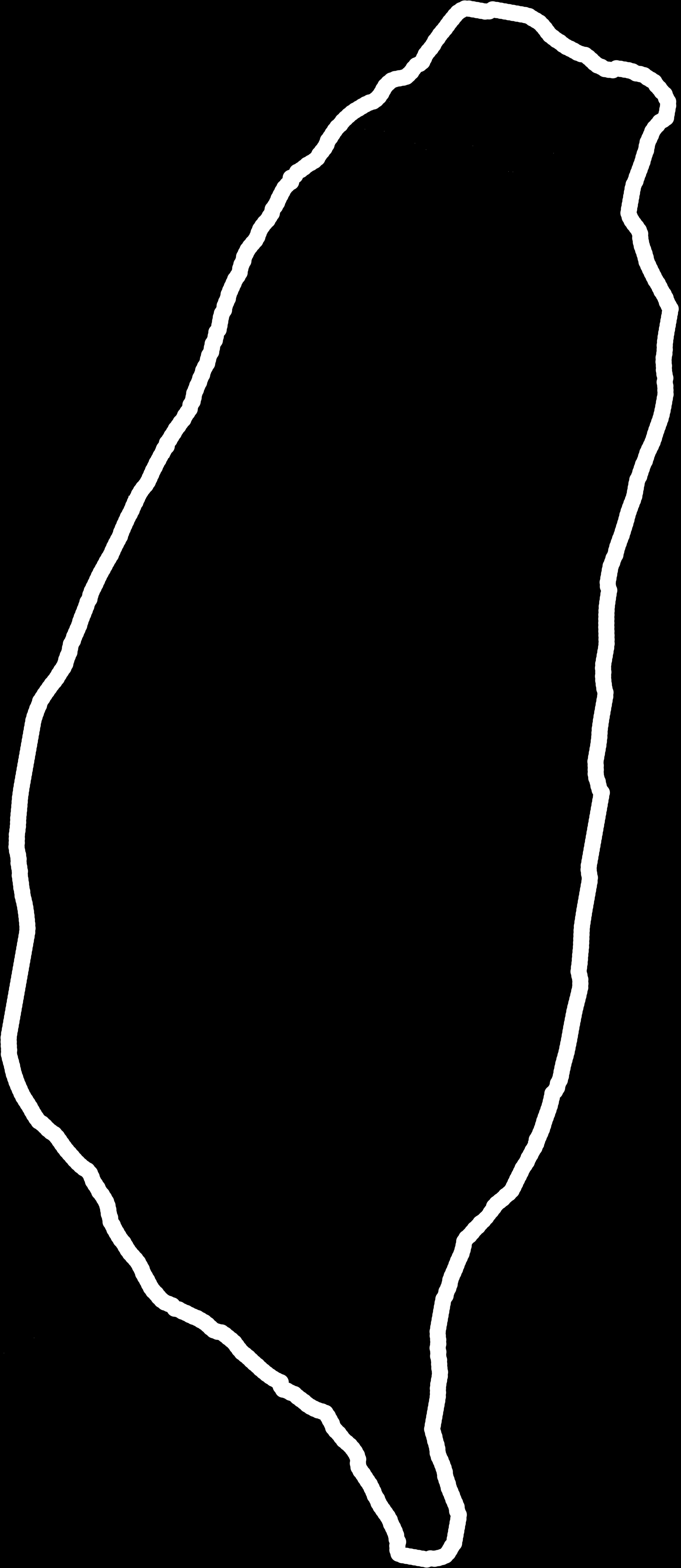
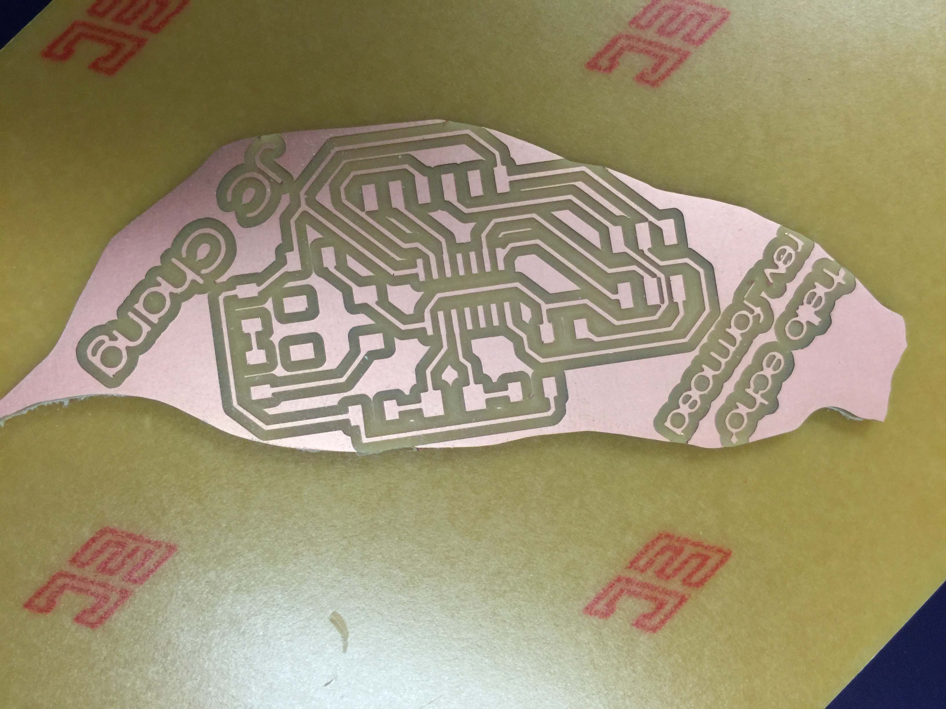
I have been fed up with retangular-ish bulky PCBs. At my previous work, fayalab, I made our breakout board series leaf-shaped, and, yes, named after leaf.

So, as you can see, I always try to add some flavor onto tedious PCB if I can. This time, contour of main island Taiwan.

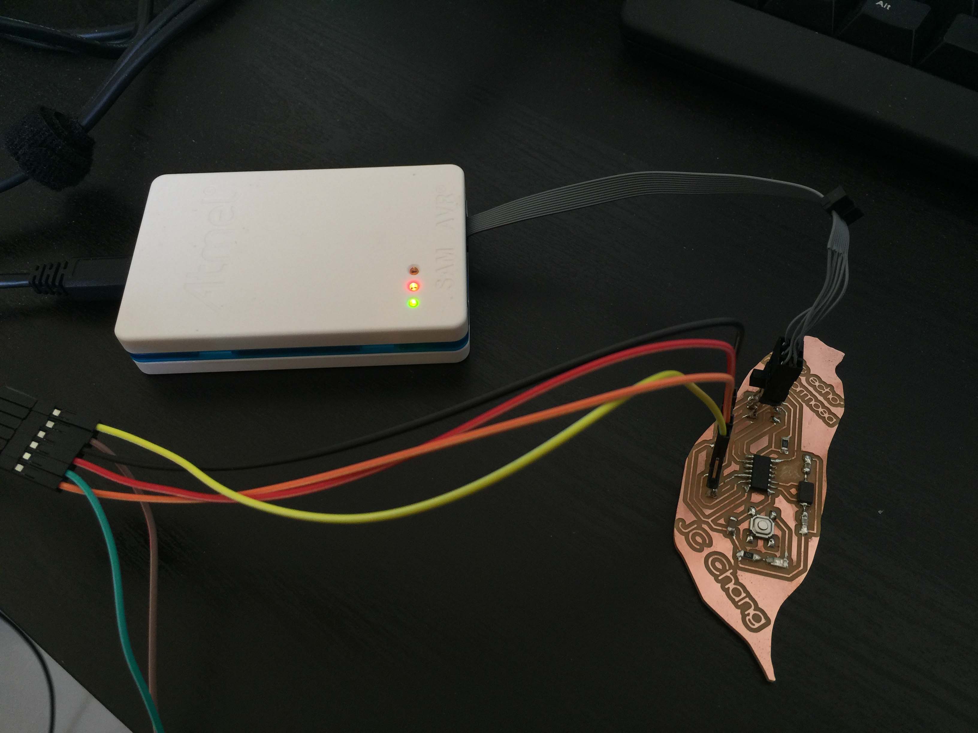
Because I cannot make the web fab module run correct path (neither guys in our lab), so I used standalone fab module to do the milling.
mill traces(1/64)
3D plane
offsets: 3
z (mm): -0.068
cut out (1/32)
3D plane
offsets: 4
z (mm): -1.4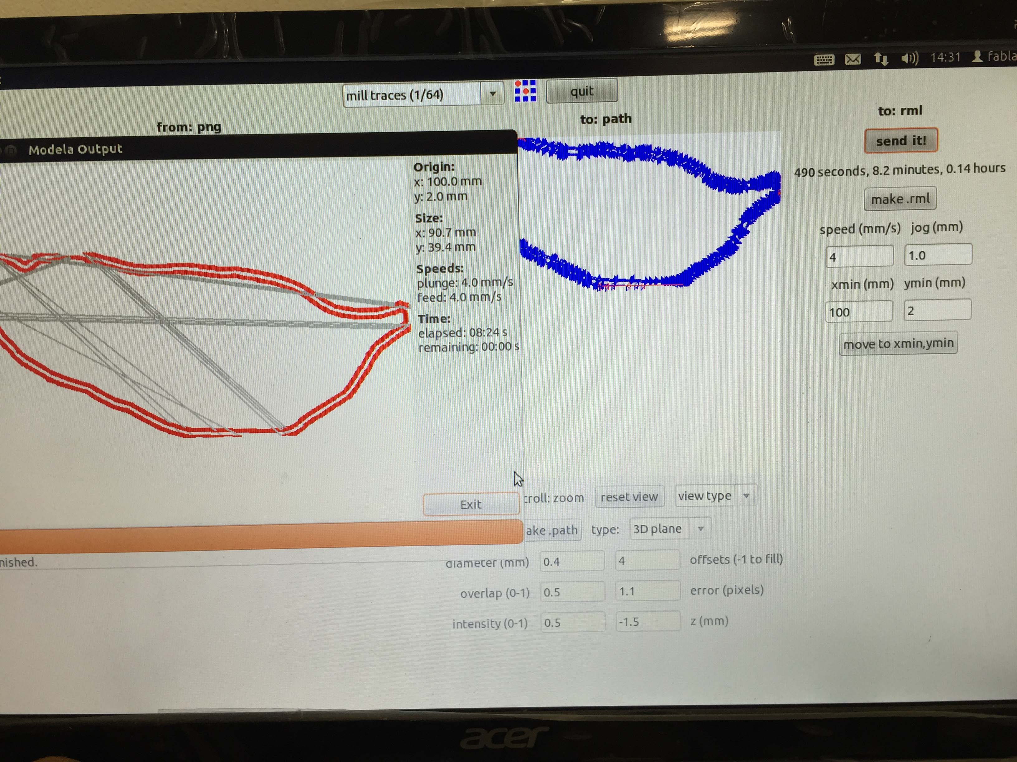
Ready for some coding!