Measure something: add a sensor to a microcontroller board that you have designed and read it
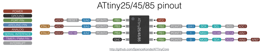
This week I chose to measure the "Light", the use light-sensitive resistor (photocell), turned the brightness signel into electric data, and then read out by the MCU. Then, using MCU to translate the input data into LED light. I used Design Spark PCB to draw the PCB and select ATTiny45 microcontroller accroding to the datasheet, there are three different models: Attiny25, 45 and 85. The difference between these chips are the RAM size. The Attiny45 is the cheapest one, that has 4K byte on-chip memory and 8MHz internal crystal oscillator. Pin2 and pin 3 can communicate with PC or external oscillator. This chip has five I/O ports: three analog inputs, 2 PWM outputs. I selected the TSSOP type, design the board by the following figure.I selected the TSSOP type, design the board by the following figure. 本周量測數據我選擇量測"光",利用光敏電阻(photocell ),將光亮度轉成電器訊號,再由MCU讀取出來。我沒有單純顯示出來,而是再由MCU處理訊號,轉換成LED亮度表現出量測的數值。 我使用前幾周(Week6)所學習的軟體(Design Spark PCB)進行電路板繪製。選用ATTiny 45微控制器,其是有小型、便宜4K記憶體的微控制器。內部更具有8MHz震盪器,低度使用下可以不用裝設外部震盪器,且可由Pin2、Pin3作為與USB通訊的端子。扣除VCC、GND、Reset(甚至可以調整成一般I/O),具有5個I/O,分別如下圖,具有3個類比輸入、2個PWM輸出,可執行許多小型專案。我所選用的是TSSOP封裝型式,由下圖讀出接腳。
To measure the light, we need to understand Voltage Divider Rule (ref. Wikipedia: Voltage divider ). As shown below, Z1 is a photoresistor, Z2 is a fixed resistor. If Z1 changes the value, V_out will change, too. Due to its internal electron irradiation of different activity, photosensitive resistance at high / low luminosity will exhibit low / high resistance. And it's very cheap without having polarity, AC / DC can be used, but the sensitivity, reliability and speed of response is it's weakness, and is affected by temperature, too. 量測光度的功能主要是利用電壓分配定則(Voltage divider rule)原理。如下圖,Z1使用可以變化電阻的光敏電阻,Z2使用固定的電阻器。當Z1變化時,V_out也跟隨電阻發生變化。光敏電阻在高/低光度時,因光照射使其內部電子活躍性不同,而表現出低/高電阻(反指標)。便宜且不具極性,交/直流電都可運用,但靈敏度、可靠性與反應速度普遍較低,且受溫度影響大。
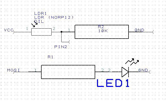
As shown above, I used pin2 as digital inputs, pin5 (MOSI) as an analog output (PWM), pin5 can be used as an output pin for LED, add one resistor to prevent burn up the LED. Schema as following figure. 參考上圖以及ATTiny 45 I/O,繪製電路時選用pin2作為˙數位輸入端,pin5(MOSI)做為類比輸出(PWM),可以作為LED亮度的輸出腳位,別忘了加上保護LED的限電流電阻,繪製如下圖。
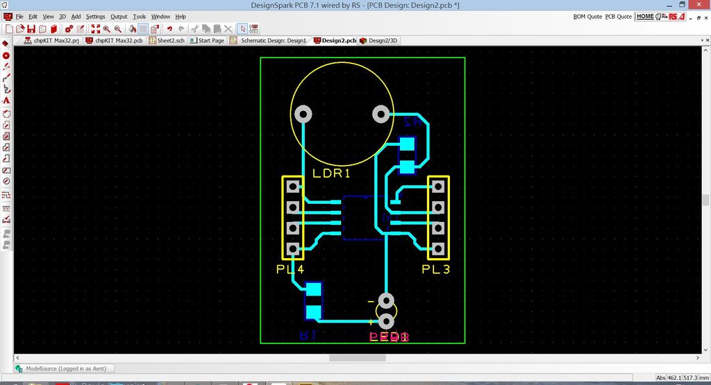
Connect the pin header with ATTiny45 for data transfering without other passive components. PCB layout as following figure. 將ATTiny 45接腳引接出,作為電力輸入及燒錄使用。單純電路不外加其他震盪器及被動元件。布局成PCB後如下圖。
Export to PDF file. 使用PDF檔案輸出圖檔。
Because some of components was not find in the SMD library, so I am mirroring the output image. Add a boarder line in the illustrator Using the Fabmodules.org to transfer the image to .rml file. Mill it. 由於部分元件還是沒有SMD library,所以輸出圖檔需做鏡射,將左右反向過來,使元件能在同一面。在illustrator中轉成PNG檔案並繪製邊框。並由Fab module轉成SRM-20使用檔案,及加工完成。
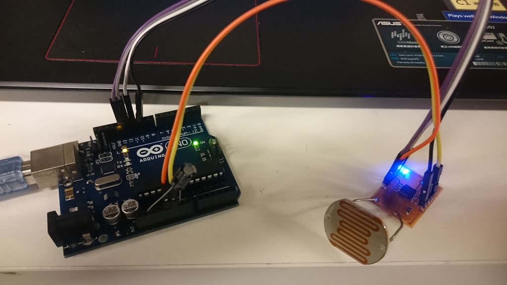
After the milling processs, welding the components. I pick a large photo resistor 雕刻完成後焊接上IC與元件,我使用了一個超大的光敏電阻。
I use Arduino IDE to program the board. ATTiny 45 is one of the AVR family MCU chip, refer to Week8s' method,Add the library into it. It all goes well. Just notice the differenct between Arduino pin number and ATtiny Pin number. 使用Arduino IDE進行編程。ATTiny 45是AVR系列晶片,參考前述(Week 8)方式,Arduino IDE新增tool及library即可順利編譯及燒錄。注意到Attiny 45腳位在arduino IDE中使用的編號,進行程式撰寫。
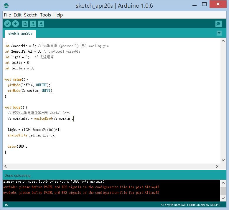
First section to define the pin number and data type.
Setup() function to define the output and imput
simply calcute the input data and write back to PWM pin.
Because the FabISP occurred some abnormal signal, I connect the ArduinoISP to write the code in. FabISP出現異常無法燒錄。便先使用Arduino ISP燒錄程式,對應Attiny 45燒錄腳位接線。
Result video. 結果如影片所示
Troubleshooting:
Because the photoresistance is too big, it's very hard to secure the component into the pcb board. Need to redesign the PCB board to secure the component. 光敏電阻太大,未於電路板上鑽孔及焊接固定。銅箔容易因碰撞撥離,可靠度不佳。
To scale down the pcb board layout, I forgot to add an ICSP pin header. connect and disconnect the wire is very waste time. ATtiny 45 腳位直接以排針引出,排列於兩側,優點是佈線(Layout)、雕刻製作容易,但沒有再做一組ICSP不易於燒率,進行實驗時總是編寫程式、燒錄、測試等步驟反覆進行,若有做ICSP將縮短拆接電線時間。
The Fab Academy is a Digital Fabrication Program directed by Neil Gershenfeld of MIT's Center For Bits and Atoms and based on MIT's rapid prototyping course, MAS 863: How to Make (Almost) Anything. The Fab Academy began as an outreach project from the CBA, and has since spread to Fab Labsaround the world. The program provides advanced digital fabrication instruction for students through an unique, hands-on curriculum and access to technological tools and resources.
Fab Lab Tainan was founded at Dec. 2013 at Tainan, Taiwan. It is the first Fab Lab at Southern Taiwan. Supported by Tainan City Government, this Lab hope could open for local citizen. The background photo of web page is the roundabout in front of Tainan train station.
I'm Jia-Hao Chang from Fablab Tainan.I'm senior staff of Association of Digital Culture, Taiwan (ADCT).In this years, I have participated the project of digital curriculum.My career is to empower people employing digital manufacturing technology or tools toimprove their problem.