Introduction
For this week we need to produce a PCB board by ourselves. There are three steps in PCB drawing: schematic designing, PCB designing and PCB making. We have made a pcb board few weeks ago so this week we concentrated on designing. I have tried three different tools: EAGLE which is free, Altium Designer which is commercial and kokopelli which is geeky.
EAGLE
EAGLE is a half-free pcb designing software. It has a commercial license but if you just want to design small PCB, free lincense is enough. Eagle has version on Linux, MAC and Windows. All of them can be downloaded from their website. www.cadsoftusa.com. Following is my turtorial for EAGLE.
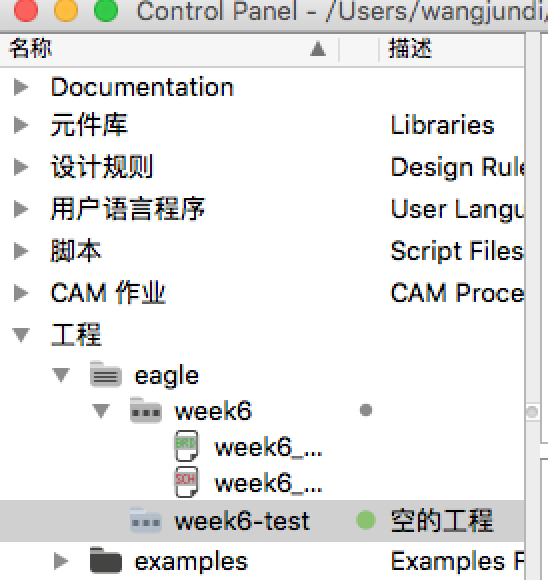
1. Setup a new project
Go to File-New-Project to start a new project. A project is consist with a schematic and a PCB borad. You have to design the schematic first them Eagle will generate some components and how their linking on the PCB board. Them you have to draw the line.
After set up a new project, you can see there is a project in the Project on the control panel.
2. Setup a new schematic
Then set up a blank schematic. Before we start drawing, we need to install the library first. Eagle Libraries consist components wa may use. For fabacademy, we have Fab library right here. Don't forget to use it in the control panel.
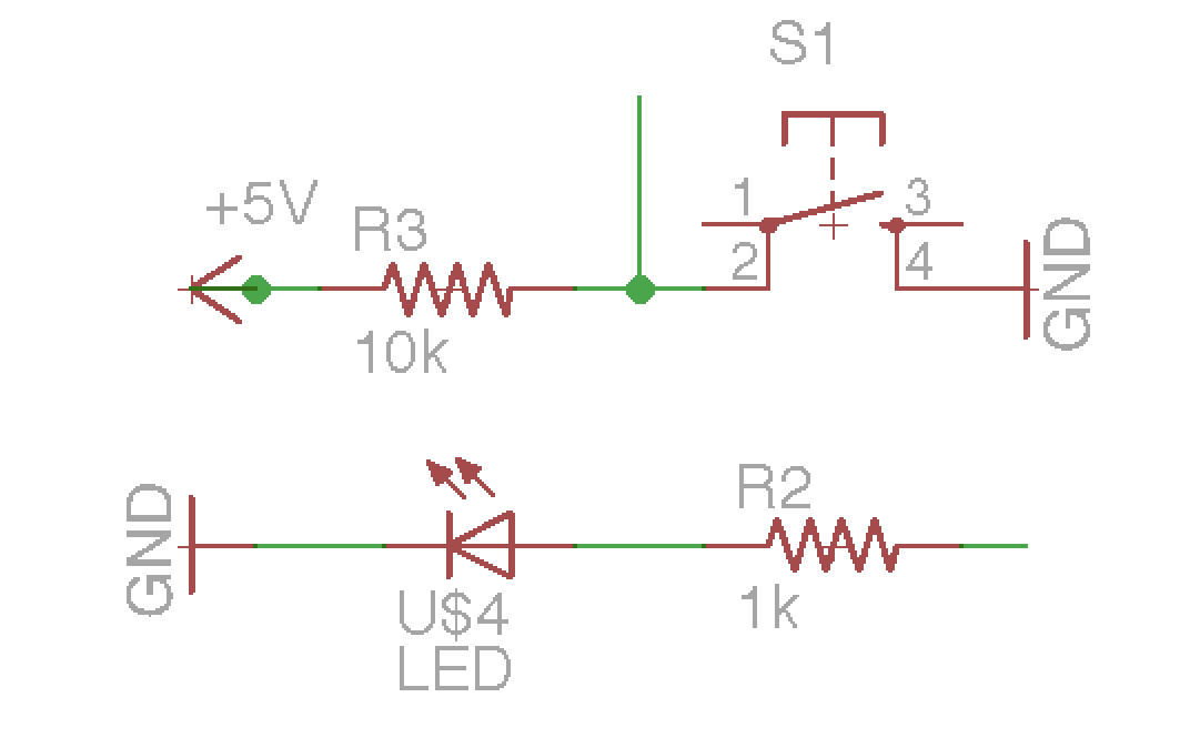
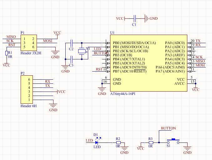
Then we can use "add" command to add components. The schematic is as follow.
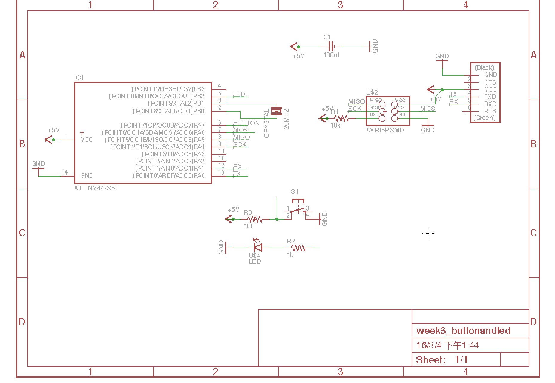
For the MCU and FTDI and ISP ports, all we have to do is link the ports one by one. For the led, we need a current-limiting resistor. Usually it is 1k ohm. For the button, we need a pull-up resistor to keep the Pin status high when no one push the button.
You can download my schematic from here.
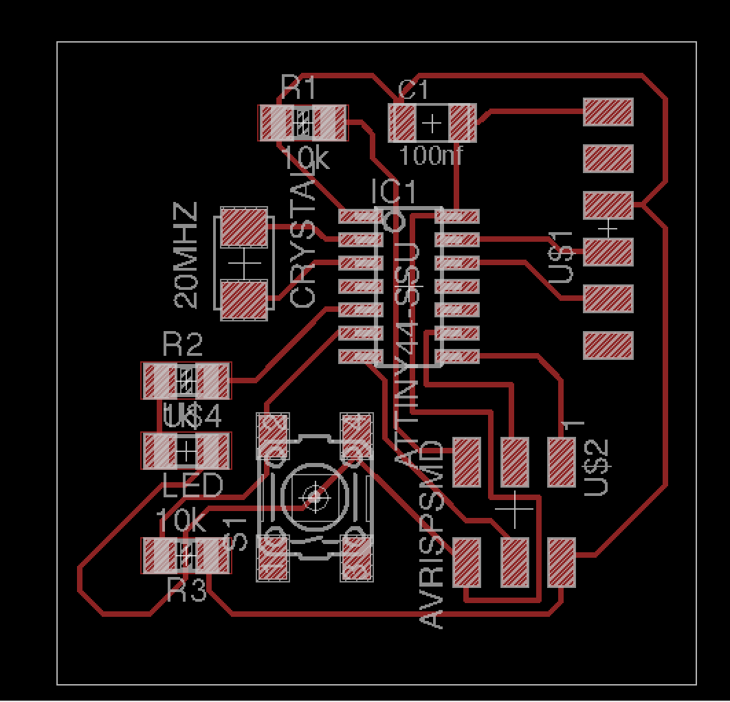
3. PCB design
Then comes the pcb disign. Click the "switch to pcb" button on the panel then you can see the board with all of your components. Arrange them and line them. Just be careful with the gap between the lines.
I have encountered some problems about the line and gap. Because the milling machine has its max precision, if you make the line to thick and get narrow gap, the fab module cannot distinguish it. So you have to keep the line thin enough and what I chose was 0.01.
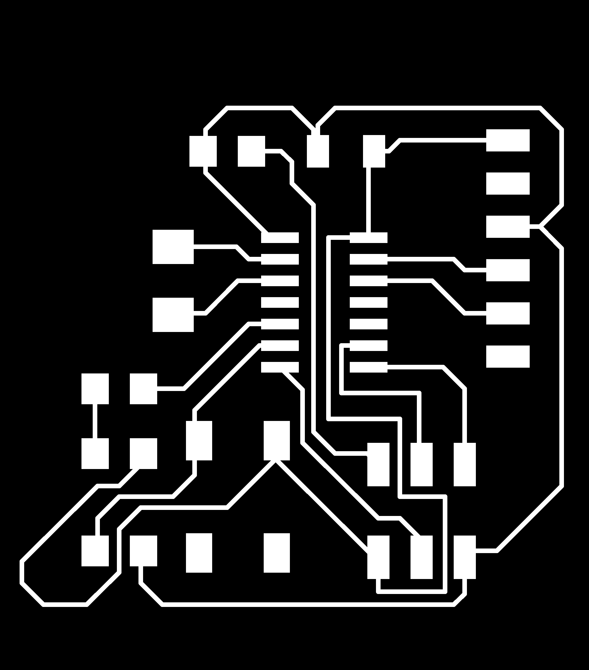
Here is my pcb board.
PCB files trace edge
And then send it to the fabmodule, mill it and sold it. Here is my final work.

Altium Designer
In my opinion, Altium Designer is far more convenient than any other PCB tools, except Cadence. But you know, it's very expensive. Thanks to my start-up company, we have an altium designer lincense. AD has the same function with eagle, but it has many assist tools to help you with the PCB design.Here is my schematic.
You can download here.
Kokopelli
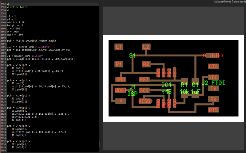
Kokopelli is a PCB design tool. It use code to design the pcb. So it's very geeky.
1. Install
Fab module local.
http://kokompe.cba.mit.edu/
Unzip to a folder open a terminal in that folder and do:
make clean
make fab
sudo make install # recommended and needed for kokopelli retro
2. Hello.button.45.cad
This file contains all the function. We just need to modify the function to make the traces. These are it's structure:
LINE 18 - 24
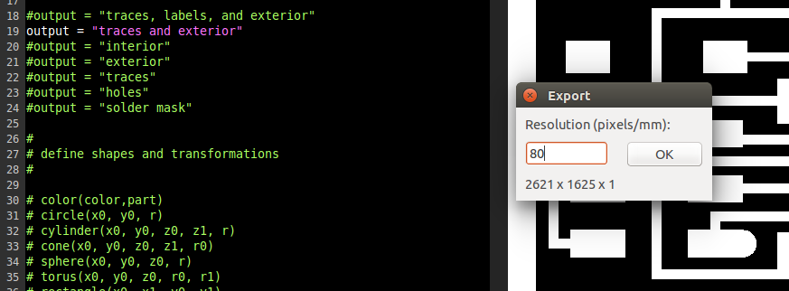
For exporting, uncoment the line depending on what output image you want. to render out.
LINE 82 - 165
Defines basic shapes 2D and 3D
LINE 172 -422
Define functions
LINE 425 - 905
Text classes and definitions
LINE 908 - 996
PCB classes and definitions. Modify the PCB class if you want to change the shape of your PCB to be eg. round
LINE 999 - 3551
PCB Library Here you find all your parts you can use, or create your own pars.
LINE 3555 -3590
Graphics
LINE 3593 - 3690
Define Board
LINE 3697 - 3714
Code for defining exporting options
LINE 3716 - 3726
Set limits and parameters
2. Adding components
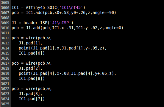
First Component a MCU ATtiny 45 and placeing it on the pcb rotated -90.
3. Wires
To draw Wires betwen components pads you first define a wire and then specify wrom which components pad to other components pad.
pcb = wire(pcb,w, J1.pad[3], IC1.pad[7])
RULE: Wires will ALWAYS be drawn, first Horizontally then vertically.
If you need to go vertically first you add a point like this
pcb = wire(pcb,w, J1.pad[2],point(J1.pad[4].x-.08,J1.pad[4].y+.05,z), IC1.pad[8])
4. Exporting
In the Export menu choose .png. You want to export a high resolution image to get the best tracing and milling result. Depending on the size of your PCB the number you put n may vary, a general rule of thumb is for a 5cm * 5cm PCB you should have around 2000px * 2000px.
But this only works with some simple circuit. If you go with a huge circuit board, tools like kokopelli will make you mad.