This
week the task was to redesign the hello world board.
I used eagle cad to do the work.
This week was interesting learning how to use
a circuit design and layout program.
I
used Neil’s sample to be able to make the schematic to see what was
needed and
added a push button and a led with a current limiting resistor. The resistor I
used was just 1 kilo ohm and
Neil recommended that for most led and could go lower if you want the
light
brighter. After
the schematic was make
showing all the connection you transfer it to the board part of the
program. Once the
board is created we
needed to use the Modella mill and cut the board the same way the
fabisp was
cut in a previous week. Now
that the
board is cut it needs to be populated with parts and with any luck it
should
work.
For
this week I used eagle for my circuit board design.
I chose this program because it is free and
has a lot of online free library’s you can add to it.
After installing eagle I downloaded the fab
library on the fab academy website.
This
library has most of the parts and footprints for the components that
are in the
fab inventory of electronic parts.
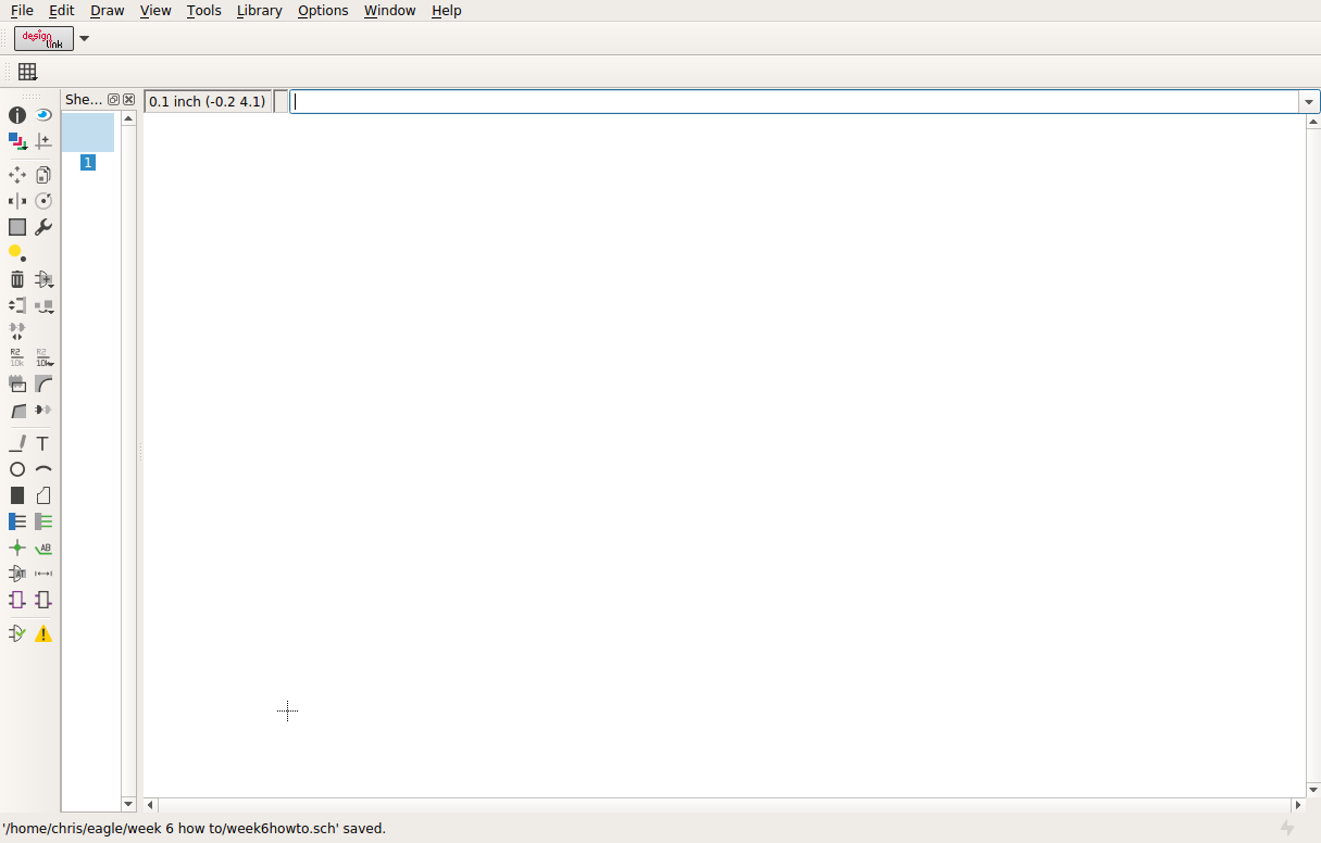
After opening eagle I created a new project to hold all my files.
After the project has been created the next step is to create a new schematic
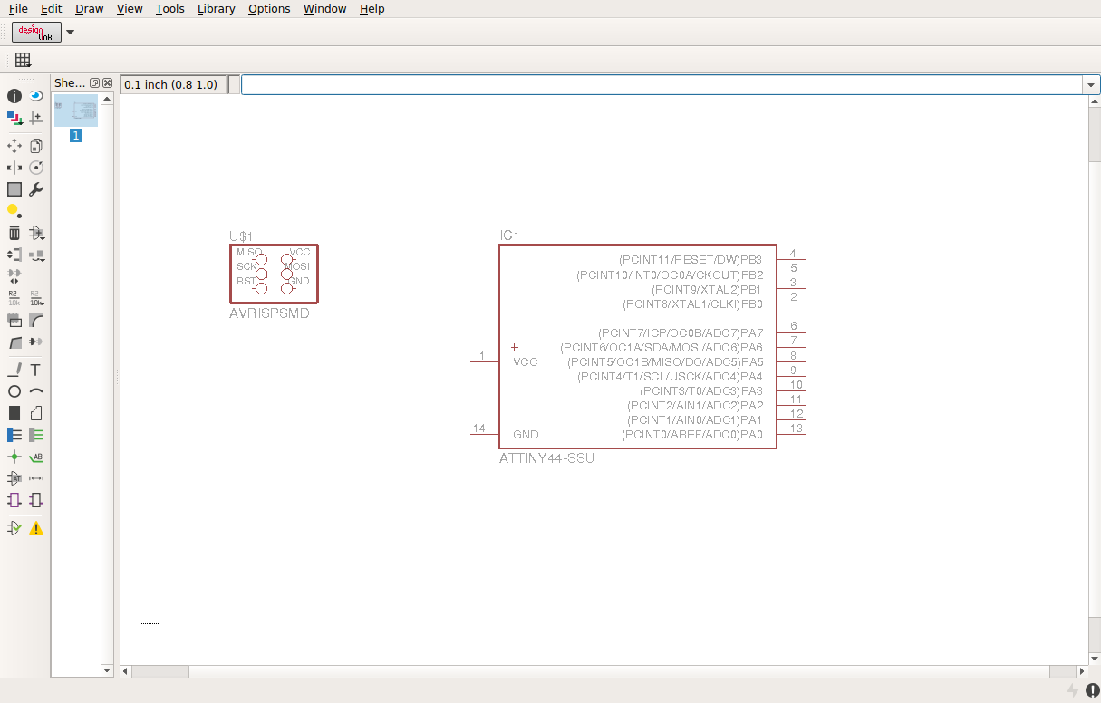
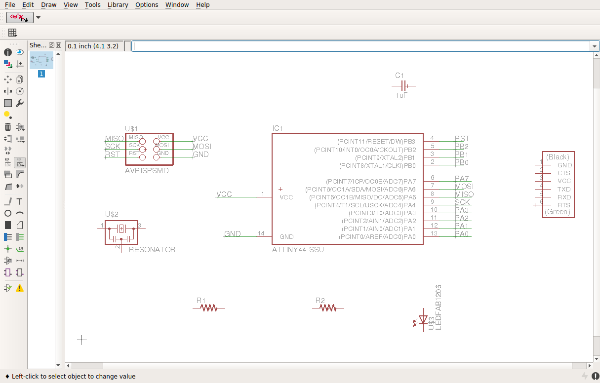
Once a new schematic is made the all the parts have to be added by using the add button. Once the add button is clicked the menu of all the library’s opens and we need to find the fab library so you can use those parts.

In the library
there are a lot of parts the hardest part is
making sure you have the right part and the right foot print. For example the attiny 44
there is 3 different
foot prints and I’m using the soic14 which is a 14 pin surface mount
package. Once the
part is selected you
have to place it on the schematic.
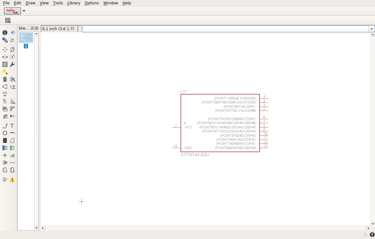
Now you need to place some more parts that need to be in the design the next part I placed was the avrisp header which is a 2x3 surface mount header.
Once some parts are added I like to some small wires off all the connections.
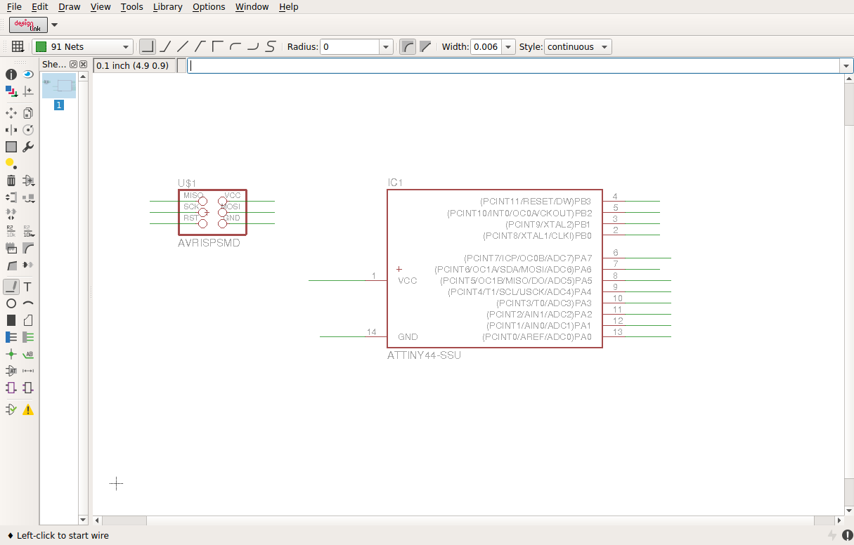
After there are
some small wires you can add labels that
will help you connect pins without drawing wires that crisscross each
other.
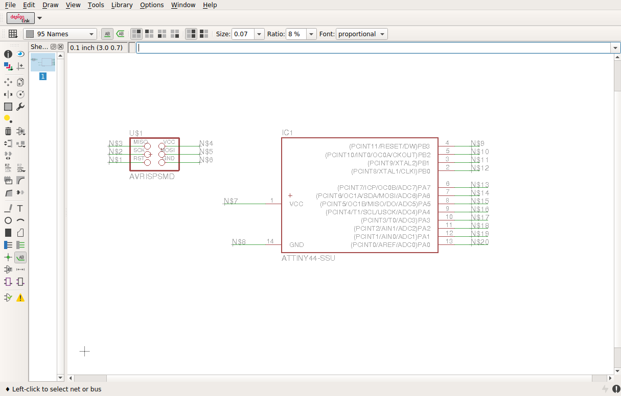
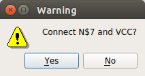
After the lables are added you need to give them a name. I named n$4 to be VCC that is on the avrisp after that I named N$7 which is the power pin on the attiny44 to VCC that will connect those two pins. If you name two labels the same it will ask you do you what these connected click yes.


Now it’s time
to add the rest of the parts and label them so
all the parts are connected.

If you right click on a part like the capacitor c1 you can change the value like 1uF.
Once the
schematic is finished you can create a board.

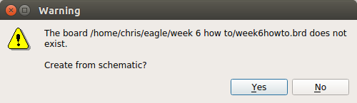
To go to the board part you need to switch to board view if you do not have board created it will prompt you do you want to make a board from the schematic you need to click yes.
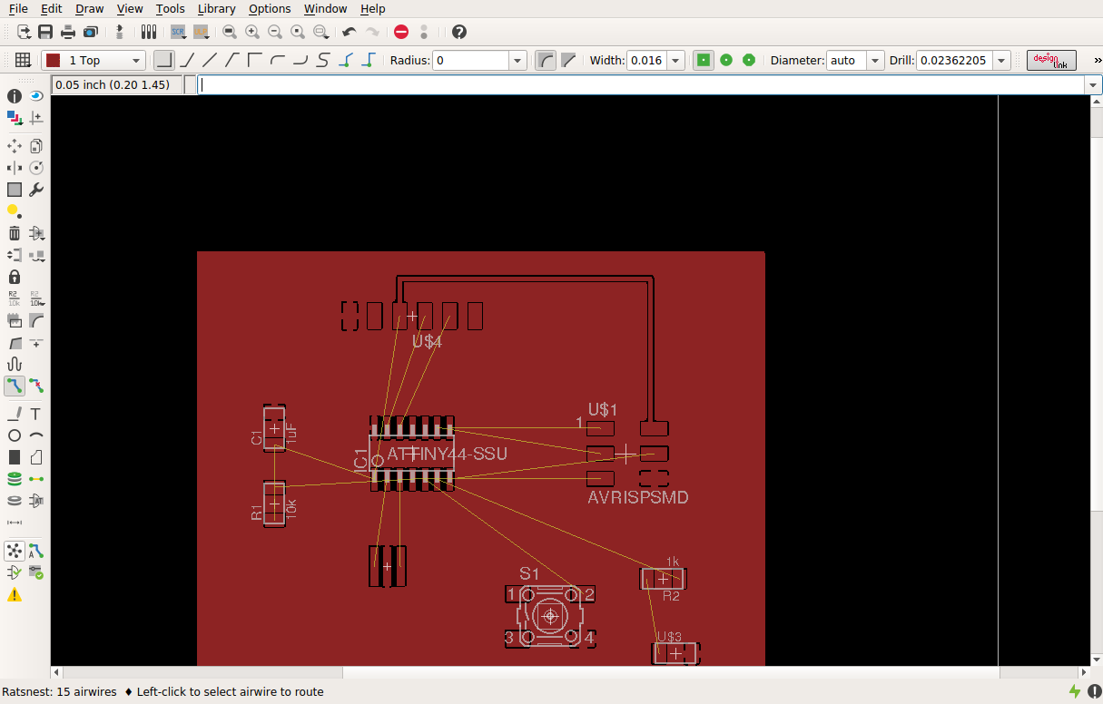
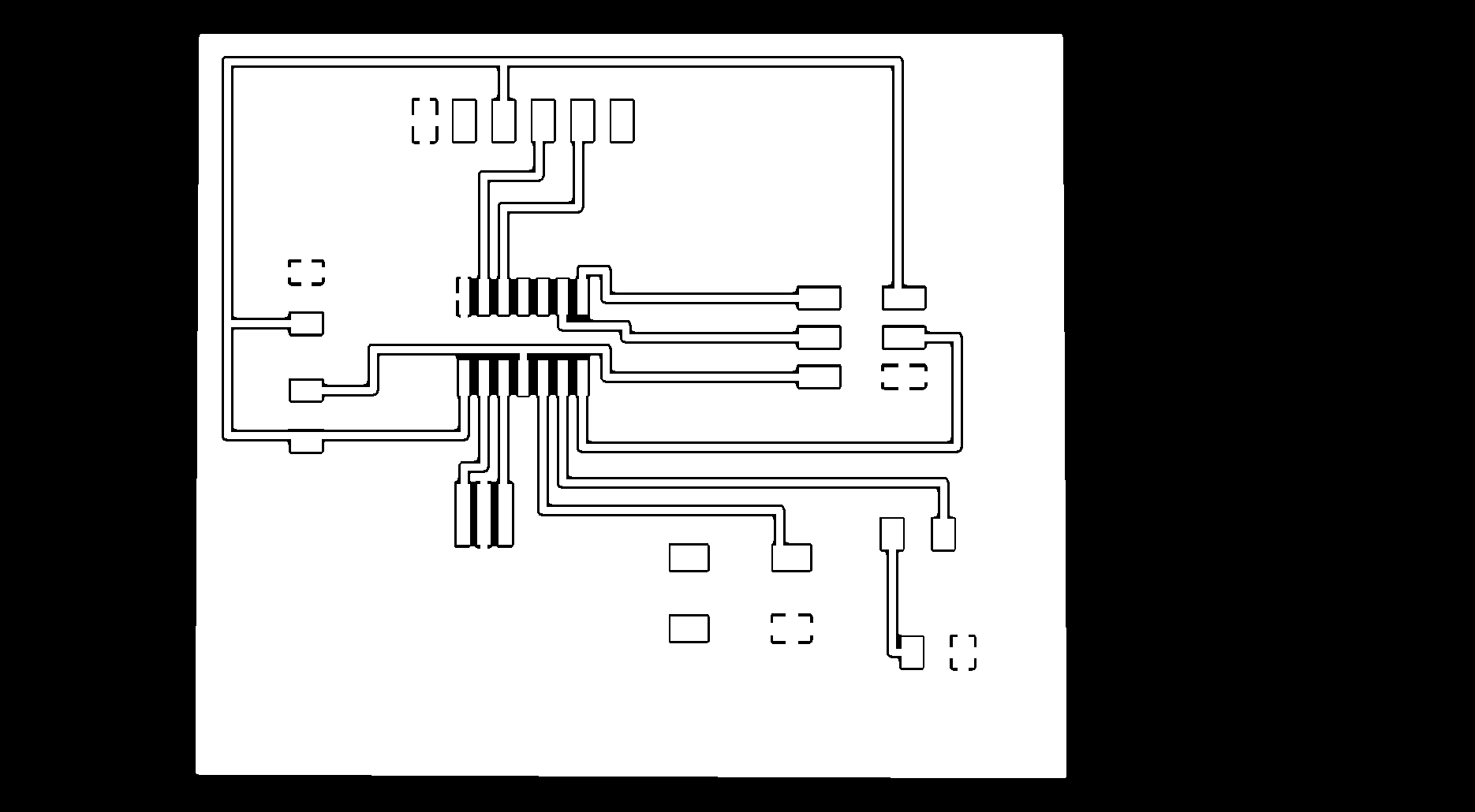
Now that the board has been created you have to place the parts inside the white square that is the usable area to create the PCB. This take time to layout correctly and may be needed to done multiple time to get it work.


Once the parts are placed initially I like to create a ground plane so that all the grounds are connected. To do this create a polygon and then name it the ground net.

Once the ground
plane has been made this is what it should
look like. All the
yellow lines are the
rats nest it shows the connection to each pin.

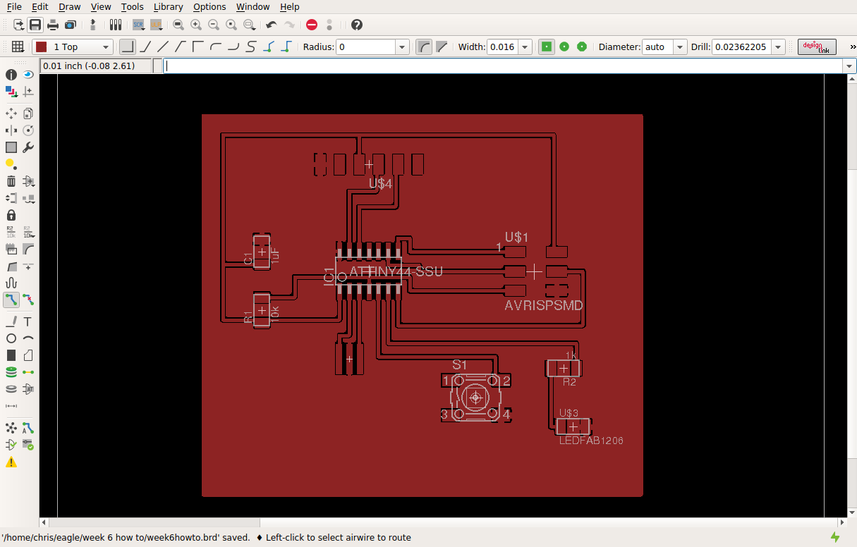
The last part
is to place all of the traces with the route
command. This can
be challenging without
cutting the ground plane or having to cross over traces which are not
allowed. There is
one thing that can
help is you can go under and between parts as long as the space is ok.

To be able to cut the board out you need to either export a png file or use the cam processor to create a Gerber file for a board house. To make a png you can go to file export and choose image. For the traces you need to make sure that only layer one or the top of the board is selected and choose monochrome set your dpi resolution and save the name. The outline of the board is outputted the same way but it is just a line so I imported into inkscape and filled the inside so there is a boarder transition to cut.

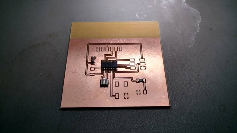
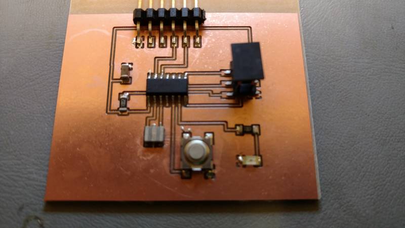
Here is a picture of the board being populated with components