Week 6: Electronics Design
Assignment
- Design a electronic circuit board with atleast one led and button
- Show how it is done with words/ images/ screenshots
- Include orginal design files
- Simulate the board
This week being Electronic Design, we are supposed to design electronic circuit board with atleast one led and button. Simulating the board is the next target.
Some software's I tried out:
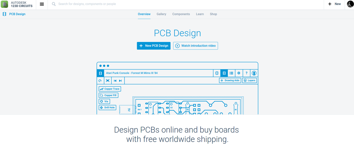
123D Circuts
123D Circut is the perfect place for bigners where we can learn electronics, PCB designing and programming. which is online based design software. Click here to get 123D Circuits
Some Features notable:
- Real Time Simulation: You could prototype and design before buiding the circuit.
- Arduino Programming
- Collaborative Editing!
In 123D circuits you can drag and drop the components. The components are listed, categorized and described well. Also, you could search for a component.
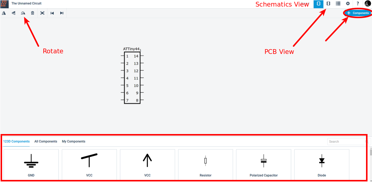
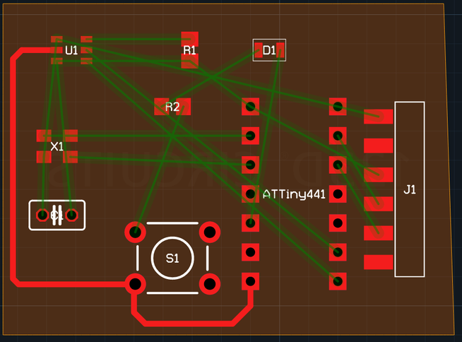
Adding components can be simply done by dragging and dropping. I dropped Attiny 44, Resistors, Capacitor LED, 6 Pin, FTDI 6 pin Header.
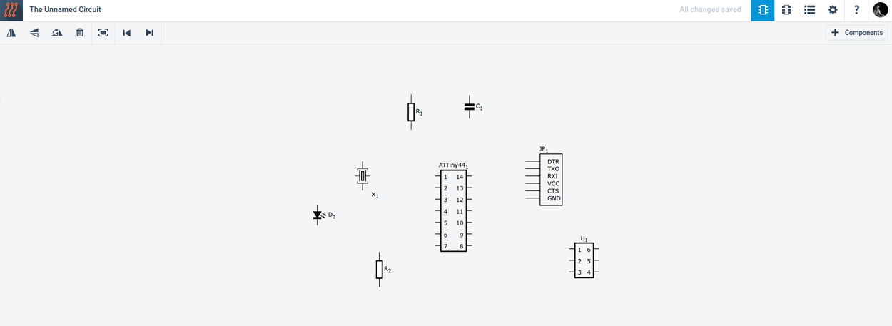
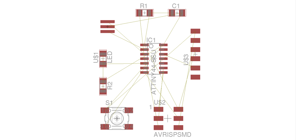
Adding components can be simply done by dragging and dropping. Schematic view after dragging the components.
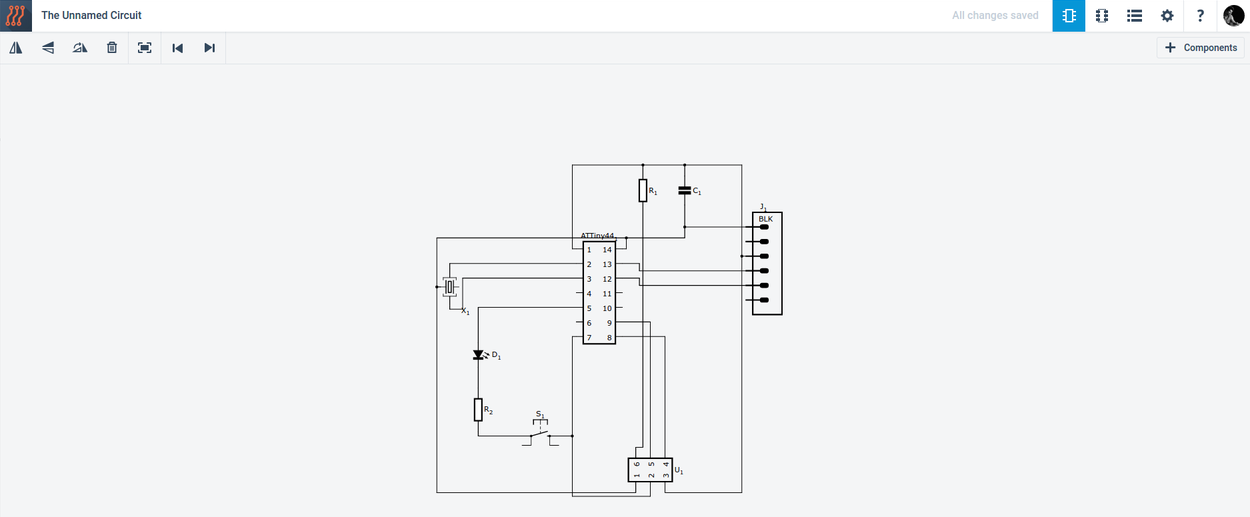
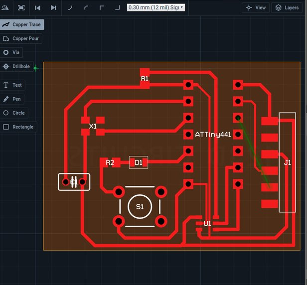
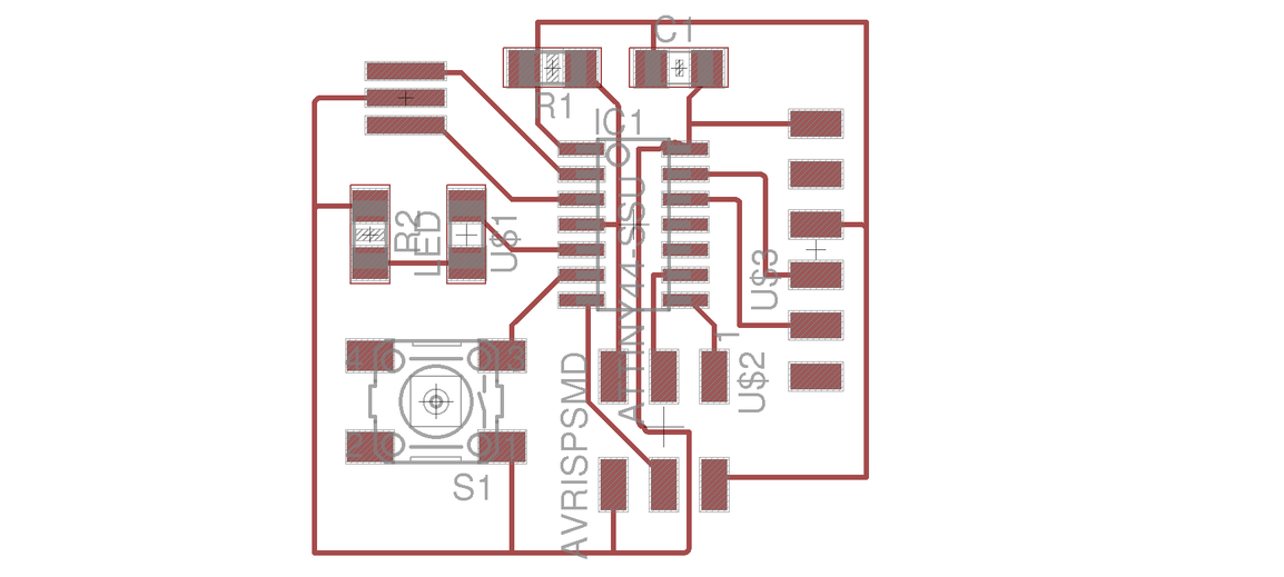
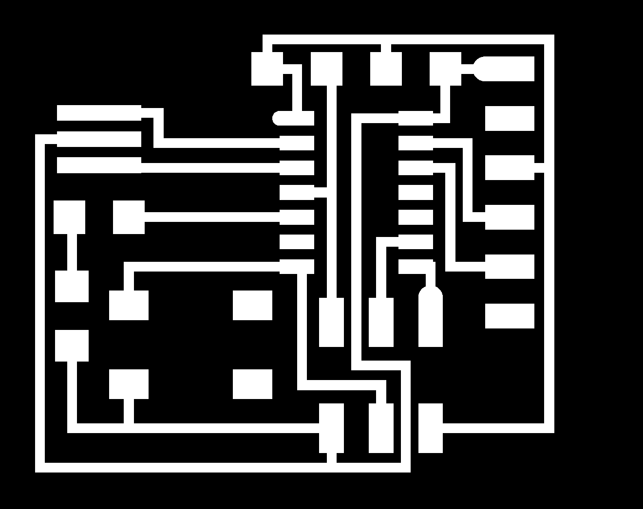
PCB view
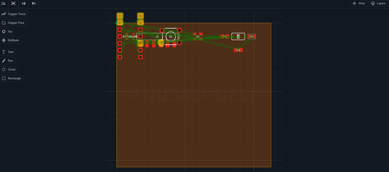
Then I drawn the copper traces
Eagle
Eagle is PCb designing software can design your board easly, I just tried this . its so simple than 123D circuit. Initialy i added Fab library to the eagle library. then I opened the new shematics (File>new> schematic)
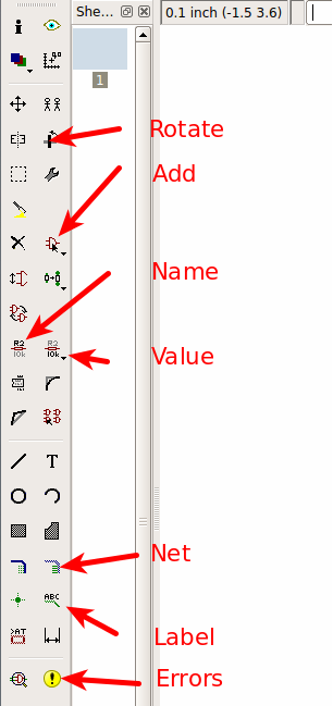
here I mensioned some useful tools for basic Pcb design using with eagle
I dropped the needed components from the fab library
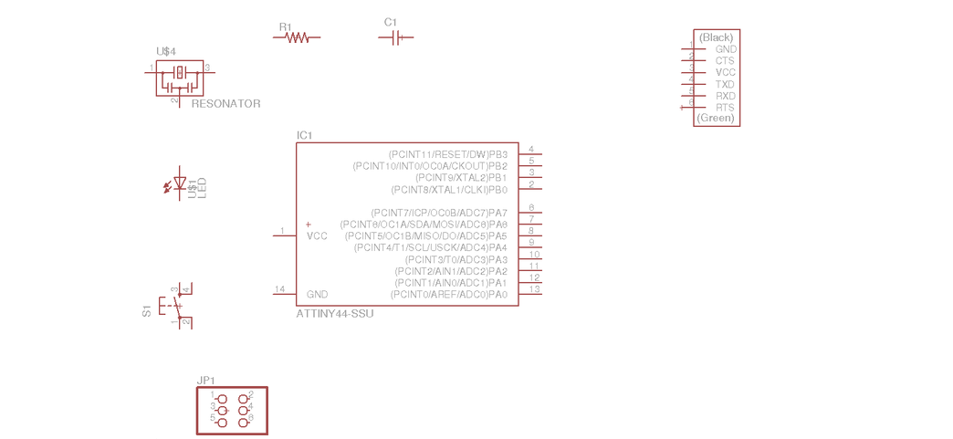
A schematic in electronics is a drawing representing a circuit. The most basic symbol is a traces, shown simply as a line.
I named the each end using Name tool with the names which want to connect. And I mentioned the values with using the Value tool
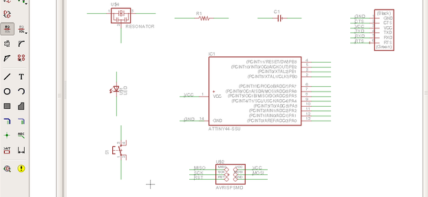
I checked the schematic Error Using Error tool. Then I switched the schematic into borad view(file> swith to board). I arranged the size of board and components.
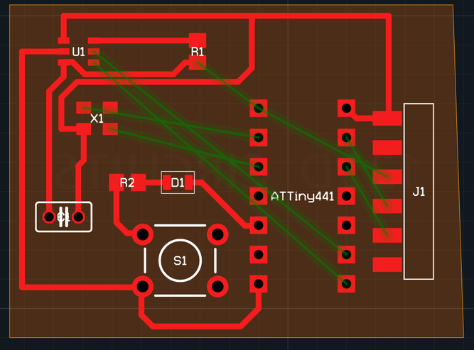
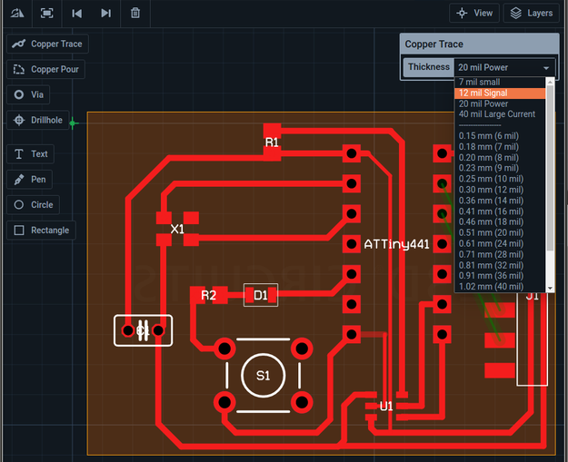
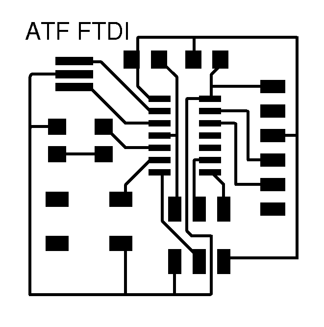
Drawn the traces using Route tool. Edited the Grid into 0.01 inch. then I compleated the full traces
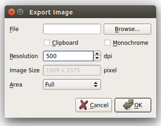
Selected the traces layer , the I tryed to export the trace and saved in PNG format.
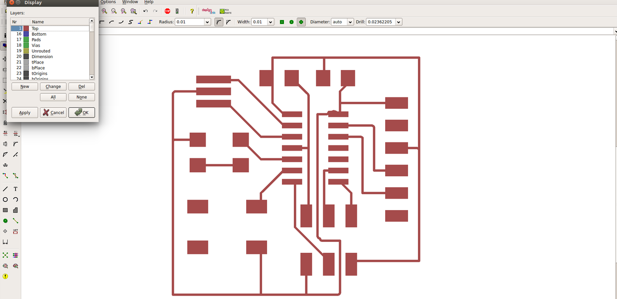
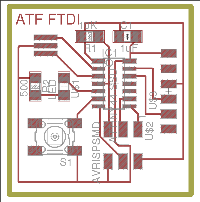
I named it as ATF FTDI drawn an exterior border with in a new layer. And I checked the error again using Error tool. there was no errors in my PCB.
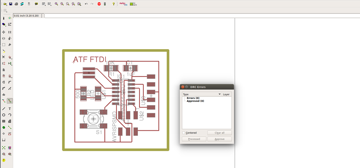
Atlast I finished my PCB. and saved it as In PNG format.


Kokopelli
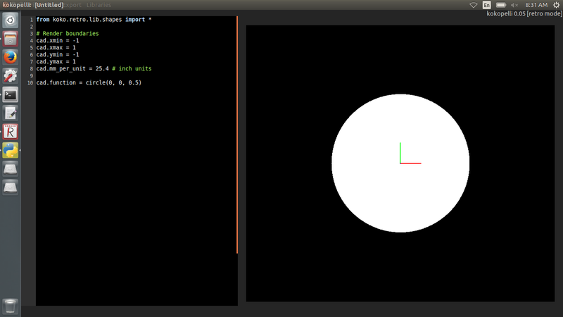
kokopelli is an open-source tool for computer-aided design and manufacturing (CAD/CAM).It uses Python as a hardware description language for solid models. A set of core libraries define common shapes and transforms, but users are free to extend their designs with their own definitions. You can also use this software for designing PCB boards.
Installing Kokopelli
First Download the Koko_retro.zip file. Then unzip it. Open the terminal inside koko_retro folder.
make clean
make fab
make install
cd bin
./kokopelli -r
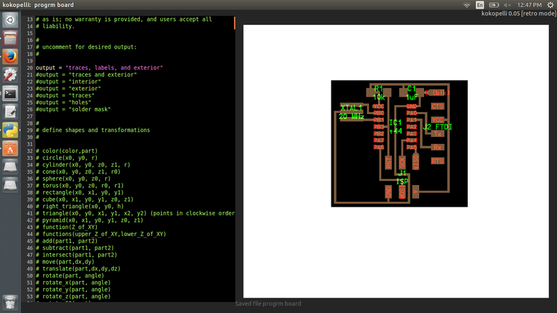
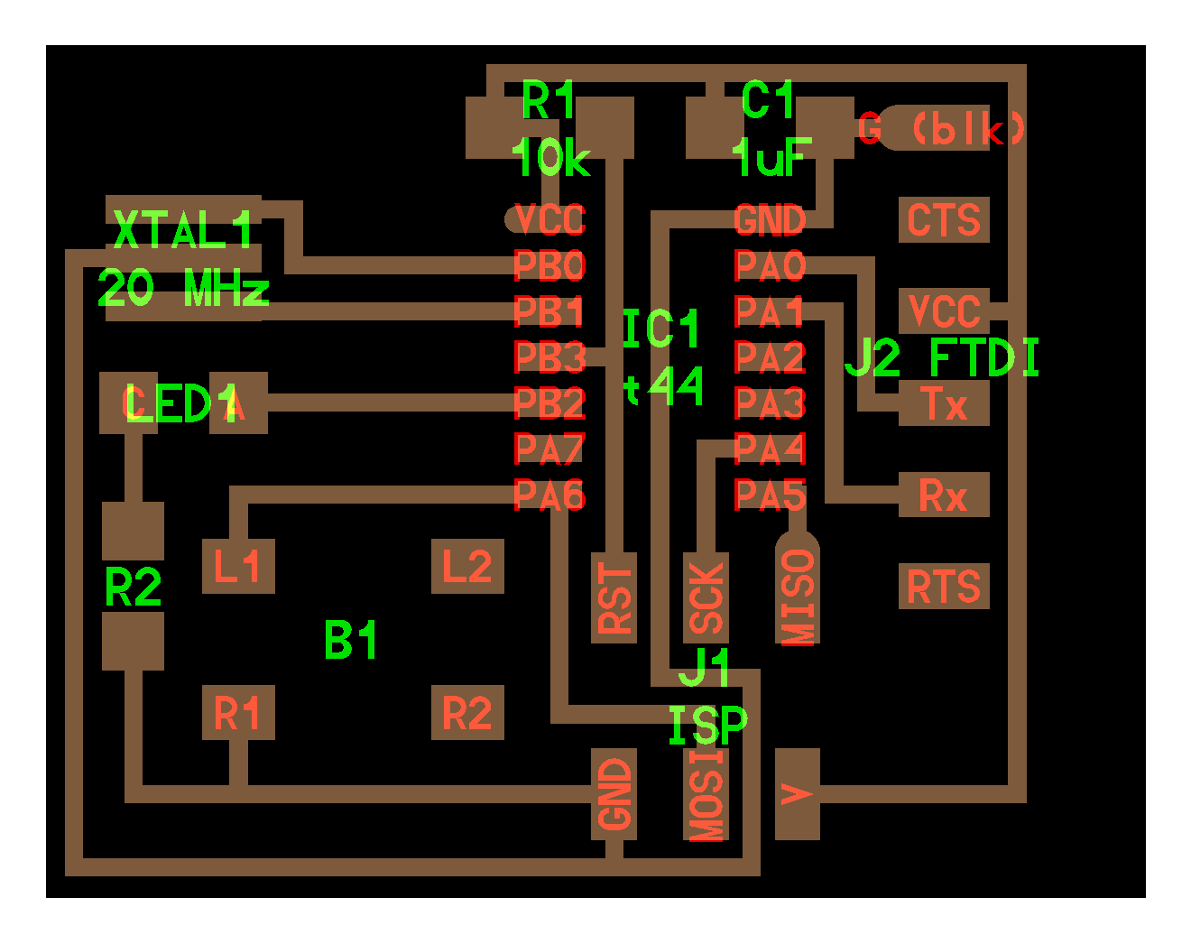
Designing Hello.ftdi
Download the program hello.ftdi.44
I pasted the program into kokopelli. Parallaly
- Open with gedit.
- Search for LED_1206, R_1206, Button_6mm
Then I need to add one LED, Resisistor, Botten . So I use these program to create the traces and soldering pints.
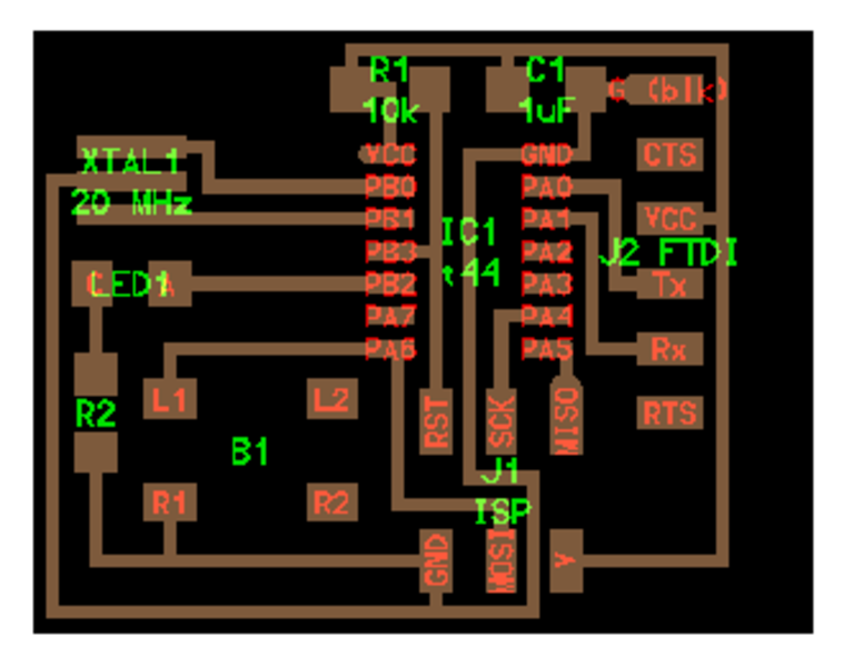
For adding the LED I inserted the following program. I want to connect my LED to IC pin 8. which denoted by IC pad 5.
LED1 = LED_1206('LED1');
pcb = LED1.add(pcb,XTAL1.x,IC1.pad[5].y,z,180)

pcb = wire(pcb,w,
   IC1.pad[5],
   LED1.pad[1])
then it shows like this
Then I inserted Resistor in between LED and Jumber(J1).
R2 = R_1206('R2')
pcb = R2.add(pcb,LED1.pad[2].x,J2.pad[6].y,z,90)

pcb = wire(pcb,w,
   R2.pad[2],
   LED1.pad[2])

pcb = wire(pcb,w,
   J1.pad[6],
   R2.pad[1])
Placed a Bush botton 6mm in between IC and J1.pad[6]
B1= button_6mm('B1')
pcb = B1.add(pcb,R2.pad[2].x+.24,J1.pad[1].y-.045,z)

pcb = wire(pcb,w,
   IC1.pad[7],
   B1.pad[1])


pcb = wire(pcb,w,
   J1.pad[6],
   B1.pad[2])
at last the PCB shows like
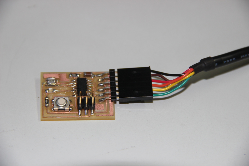
I milled and soldered the board.