PLEASE NOTE: Final Project Experiments involve weeks for:
- Input = Motion Sensor
- Output = LED Array
- Embedded Networking and Communications = programmed serial bus
- I also edited Neil's C and Make files from those weeks to develop a proof of concept for my device, which combines goals for those weeks as well.
- Completed Schematic Drawings
- Completed Board Layout Designs
- Noting my process/progress as I work
- Scaling/importing my drawing/design images (get it right in the design and you don't have to go "back to the drawing board"
- Milling and stuffing the boards - 3 in total: the bridge (has the FTDI) and 2 nodes, all boards have 4 and 6pin headers
- Programming the boards in C
- Video the results
- I omitted the tiny45 and replaced it with the tiny44 micro-controller.
- Don't make your traces in the schematic - just make the connections. I used the net tool as opposed to the wire tool because I had the bad habit of criss-crossing lines that weren't clear as to what was connected to what.
- If you're frustrated with the lines (routing or wire) snapping to the grid lines, visit the grid icon and select 'finest' for display and style. Note that you'll have to increase your resolution and/or trace your lines or adjust their width to make sure they can be seen well by the modela
- Then I used the move tool to literally move the lines to an angle where I could clearly see what was being connected.
- I used the tiny44 micro-controller datasheet to make sure I knew what pins did what, and how they should be connected to the 6pin header.
- Then I looked for a board Neil had routed and uploaded, that connected a tiny44 to a 6pin header => and used that as a visual template to draw from.
- I left the connections open for the following components because I wasn't sure how easy it would be to create the board layout and I wanted to leave myself a loophole for connecting: Resistor1, the LED, the switch (Omron Button) and transmit/receive on the 4pin header, to the micro-controller.
- Eagle won't let you route connections on the board layout if your connections in the schematic aren't right! You'll want to adjust the board view by zooming in and out while drawing to make sure you're connecting the components.
- Before you do anything, save your work in a place you can find it!!!
- Click the layers settings icon (go to help in the Eagle toolbar and type the icon name you seek and the program will point it out to you)
- Choose 'none' in the layers window
- Click apply
- Click 'top' and 'bottom' - to maintain your image's traces - then 'ok'
- Go to File, then Export, then Image
- Name your file
- Click Browse to determine the file path to save to
- Click 'Monochrome'
- I raised my resolution to 1500 so that my image's traces will show up in the modela's preview window (the image size rises automatically)
- Click apply, then 'ok'
- From here, you can upload your image from its saved location to Fab Modules
- Fab Modules allows you to invert your monochrome image so that it can be directly milled via the modela!
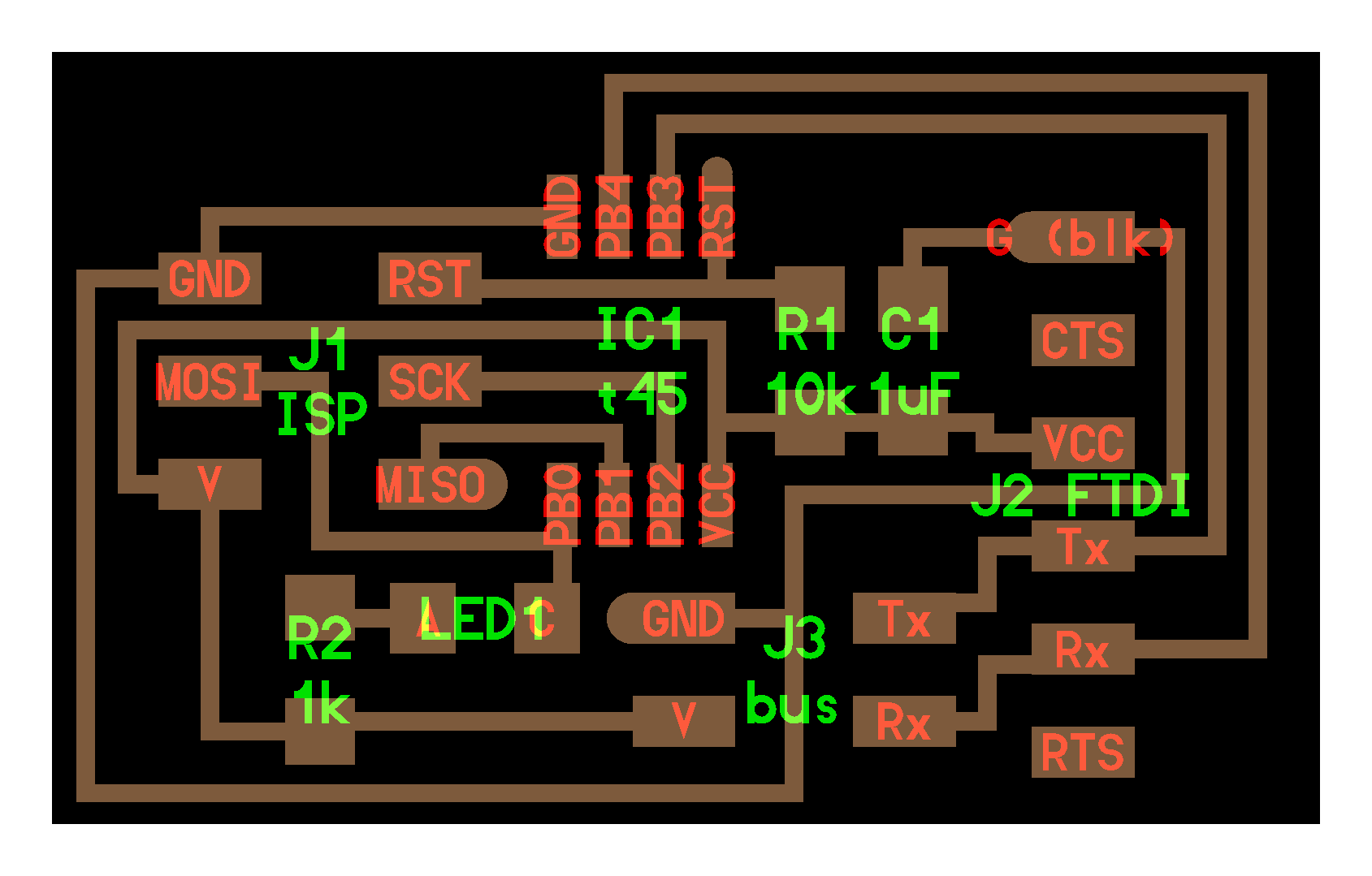
Designing Schematics and Board Layouts for a Serial Bus System
I wanted to create a bus system LED and motion sensor components. The boards are to light up when motion is detected. This would combine the assignment weeks for: Electronic Design, Input Devices and Networking and Communications. This would also create a working prototype for half of my final project.
Workflow Goals:
Designing in Eagle 7.5.0 Light
Drawing the schematics was much easier than designing the board layouts for me. I sometimes would pick the wrong components (surface mounted items are red while drill-holed items are green and white), but I knew the purpose of the drawing was to create a precise representation of the actual circuit board to be programmed. Here's my process:

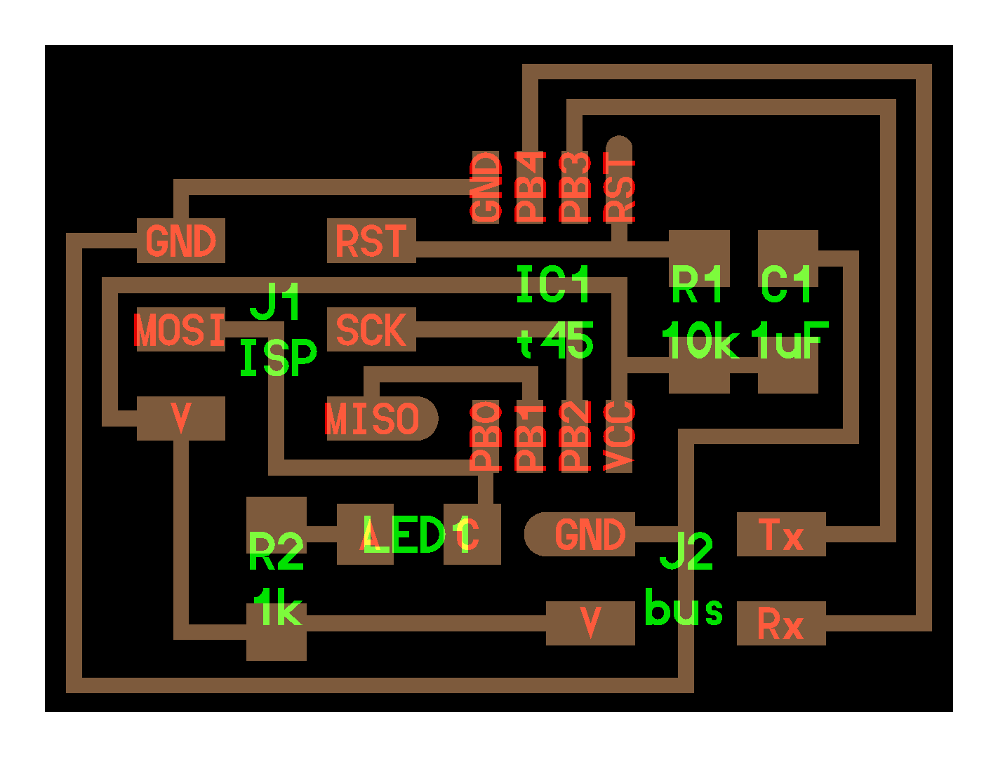
The above schematic is my re-drawing of Neil's hello.bus.45.bridge board. Below is the corresponding board layout, as traces:
Please note that wires were added due to a missing trace on this re-drawn board.


I was able to draw those on my own but when it came to adding/subtracting components for the other boards, I ran into problems, especially with the board layouts. I kept isolating power and ground on my micro-controller, making necessary components obsolete because the pins weren't accessible - too many bad moves wastes precious time:

I sought help from our lab coordinator, Zuberi Moore, and learned the zen of circuit board design. Here's the schematic and board layout for my bus node (this link connects to Neil's design), with a few exceptions:

Here's my chicken scratch with pen & paper -it helped me figure out how to route my traces! But so did the auto-router tool. I used it 4 or 5 times actually, while zooming in to edit traces that were too close to the component pads and deleting wacky connections.

To turn off Layers
Exporting the Image:
I've learned A LOT this week and look forward to applying this knowledge to my final project!
Types of USB cables: http://www.velocitymicro.com/blog/usb-3-1-vs-usb-type-c-vs-usb-3-0-whats-the-difference/Input: Motion Sensor & Output: LED Array
My simplified experiment that was successfully completed in the week for Networking and Communications, offers a rapid prototype for an initial iteration for a full scale device: The LED strips will be connected to the circuit boards (which will be encapsulated in waterproof material doubly), which includes the motion sensor and phototransistor. Solar panel(s) and an external battery will also be added during the spiral development process, as I scale up to a fully functional device.


Here's a video of my proof of concept via video