Week 04:
Electronics Production
Important Vocabulary
Tiquismiquis: Escrúpulos o remilgos afectados y excesivos
Objectives
- create an in-system programmer to hold a small amount of code: requires milling a new board, soldering, programming it, and documenting the process
Software
- FabModules for .png to AVR
- AVR Crosspack for the firmware that is permanently on my ISP.
- Makefiles, with Xcode to run.
Machines
- Roland SRM 20, the «MonoFab»
- Modela mill
- ATAVRISP2 programmer
PRACTICES
How to Mill and Program a PCB
(although this stands for printed circuit board, the boards are usually etched or milled; also, PCB is how the substrate is referred to; when it is "stuffed" with components, it is a usually just called a "circuit board")
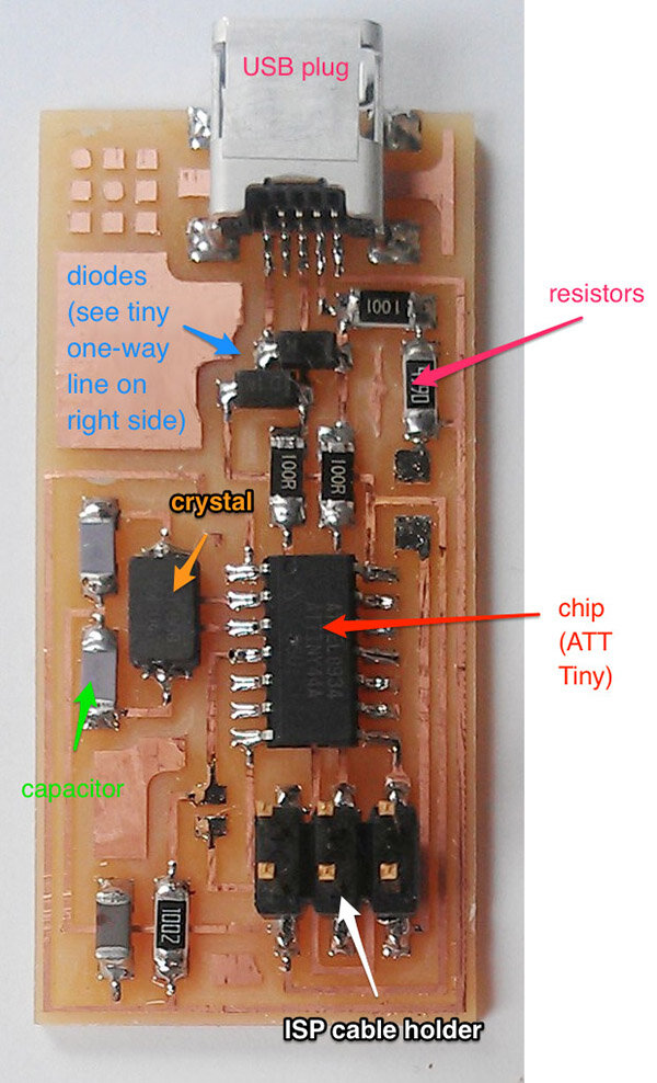
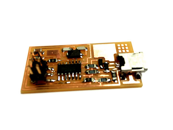
I am making a copy of Neil's programmer, which will allow me to keep a small amount of code / text on a homemade ISP (in-system programmer).
To Mill
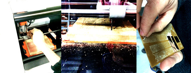
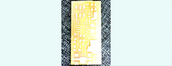
A milling bit drills off the veneer of copper, leaving copper in place to form electrical paths. Here’s everything we need to know to do the work:
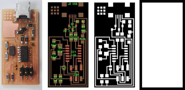
Two .png files control the paths that the milling machine will use. A fab module converts the .png into paths that the Roland SRM-20 can read.
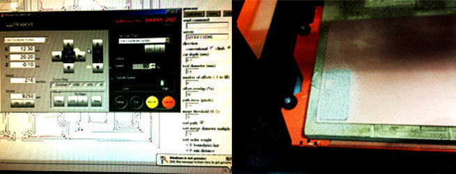
For our in-house milling machine, the first thing to do is to make sure the bed is *f*l*a*t.* We are milling .1mm at a time, so perfection becomes relevant. After carefully setting the delicate 1/64” (.4mm) milling bit to zero, during the first board, the PCB pulled up off the bed. The board was stuck to the bed with double-sided tape. We decided that the underlay needed to be more flat, so we re-milled the entire surface, and had a tape-removal party so we could put on fresh tape.
Our fab module was acting up in conjunction with the machine, and the monoFab kept irrationally stopping. A babysitter had to press “resume” whenever it queried. Demanding kid.
After the traces are milled, you change the bit to a thicker one (1/32”, or .4mm) in order to cut the outline. With this bit, we set the step-down each time to .6 (as opposed to .1 for the traces). The material itself is 1.5mm but we set it at 1.6 so that it cuts through (and into the underlay; hence why the underlay needs periodically to be re-milled); the fab module automatically goes around twice and then adjusts the last trace to go around the remaining increment, which in this case was .4mm. THIS IS DIFFERENT FROM the “OFF-SET” number, as we discovered. For the traces, you offset 3 times; for the outline, the offset = 1.
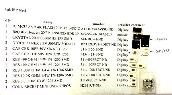
Using the schematic, we picked parts from our “electronics closet” (a bunch of madly minutely labelled drawers in the FabLab) and used tape to affix the parts to our parts list. Nifty trick to keep track of each tiny necessity.
Moving into soldering ...
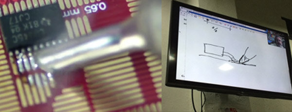
Neil made a drawing showing the importance of heating the pad and the component to get a good weld. Ferdi recommended a fantastic tutorial on soldering ~ I thought the multi-pin soldering, with a flux pen and a well-tip gun, was especially cool.
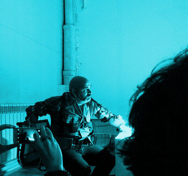
Below, see the eerie shot I took of Jisun at work under the lamp + magnifier unit that helps us see the parts.

I find this process beautiful. Bright lights, shiny solder, magical chemical transformations ...
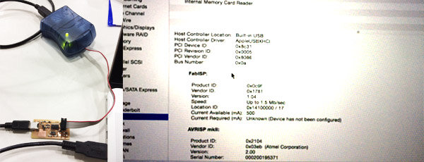
Then, using a Fab Academy tutorial for programming , I used an AVRISP as the programmer to program my programmer. The only thing to note here, really, is that the Makefile contains code to program BOTH the ATAVRISP2 and the FabISP. We are not going to both at once, only one at a time, so use the hash to turn one of the lines into a comment while the other is a command.

The last step for this week was using desoldering braid to pull the 0-resistor jumpers off, transforming the board from a receiver of information to a giver of it.
N.B ~ IF it hadn’t worked, the troubleshoot is to take an ohm-meter and methodically go through all the connections based on the schematic, making sure the meter beeps when traces are supposed to connect, and that it doesn’t beep when the meter is touched to things that are supposed to be separate.
Theories
Ferdi said a nice thing that reminded me of the pedagogical philosophy of Sugata Mitra’s Hole-In-the-Wall project in Kalkaji, Delhi: you make the thing, and it works, then you start to wonder why it works. This is so different from compiling knowledge in order to act. In Fab Academy, we act, then we take whatever time we can make to figure out what we just did. I think this is Ignorant Schoolmaster in action … Mitra calls it "miminally invasive education."
EVENTS THIS WEEK:
IAAC winter lecture: Marcellí Atúnez
He's a wild, bold, insane, pornographic cyborg artist. My takeaway: bust it up. Work harder to break all the boundaries. Do it with fierce horrific breathlessness, a suffocating sense of sexual excitement. Not because it's (gack!) good or useful!
Okay, I immediately capitulated to my impulse to be good and social. I threw a party at my house for the lab.