Exercise 6: Electronics Design
Starting out with Eagle CAD
3/02/2016
I just finished making my first circuit board using Eagle CAD following the tutorial from OtherMill click here . It was relatively easy to follow the directions but obviously I would be pretty challenged if I was asked to design a board from scratch.
I learned that the first thing we had to do was make a sketch. The hardest part of this is finding the correct part from the library. One minor problem I found early on was connecting components on a circuit board. I had connections that should not have been there and others that were not.
When I checked my original sketch it seemed to match the tutorial picture and I tried fixed the lines but it did not seem to make any difference so I just started over.
When I drew the lines correctly the second time it worked and looked like the picture in the tutorial.
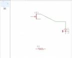
I then had to the sketch the board. The lines were all jumbled up between the components. According to the tutorial these are just air-wires and not traces. As shown in the tutorial we could use the select tool to move the components around.
Once I did this then I used the Auto-router tool. I do recall Neil saying that this often causes problems but this is a simple board so I tried it and it worked. It rearranged the connections so that the traces made more direct paths. The only thing that had to be fixed, per the instructions, was the LED. I also tried doing it manually and it was very easy.
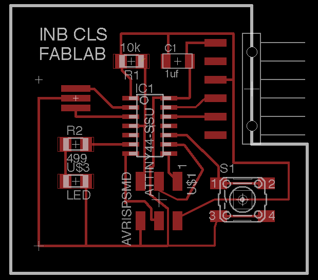
Designing the Hello World Board
The next thing I worked on was finding the components to make the Hello world board for the FAB academy. I looked in the existing library Eagle CAD and most were in there.
3/3/2016
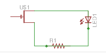
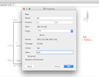
I worked on Eagle for a very long time today. Getting the FAB library was a huge help. I found most of the components on the FAB library. One of the first things I learned looking through the Eagle library was to tell the difference between components that will have holes and those that are surface mounts. It took me a little while to figure out that basic components like ground and VCC were in a in a library called Supply. Once I did this it was pretty easy to find all the components. The only component that I had a hard time finding was the JP1. After looking extensively for it I cut and pasted this one component from an earlier sketch by a previous FAB Lab student.
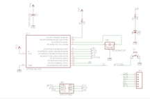
The next thing I had to do was label of the connections. This required drawing a line from the components that matched the example board. Then I had to name and label each wire. I had some trouble with this because I kept left clicking on it the line to select it and then right click it. This would not bring up the menu for selecting label and name for the wire. I realized that the problem was that you only needed to hold the arrow over the line and then right click. I thought it was pretty cool how once you wrote the name it would connect the various components. It was however pretty frustrating because I had no idea why most of the were there. I hope to gain a better understanding of the why and how of circuit boards are configured.
The other similar problem was moving groups. I knew to use the group button but I could not get the move group option to come up. I realized that Eagle gives you directions at the bottom and it instructs you to hit control and then right click to move a group. Once I figured out these things it was pretty easy to make up the rest of the board.
Once I had all the components on the schematic setup I switched to board. All the air-wires were crossed in every direction. One thing I did was to stretch out the air-wires to better see where everything was connected.
Because I had no idea where to start or really even what I was supposed to be doing, I decided to follow the protocol I did with the the othermill lesson. So I first tried the Autorouter function.
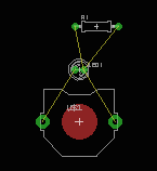
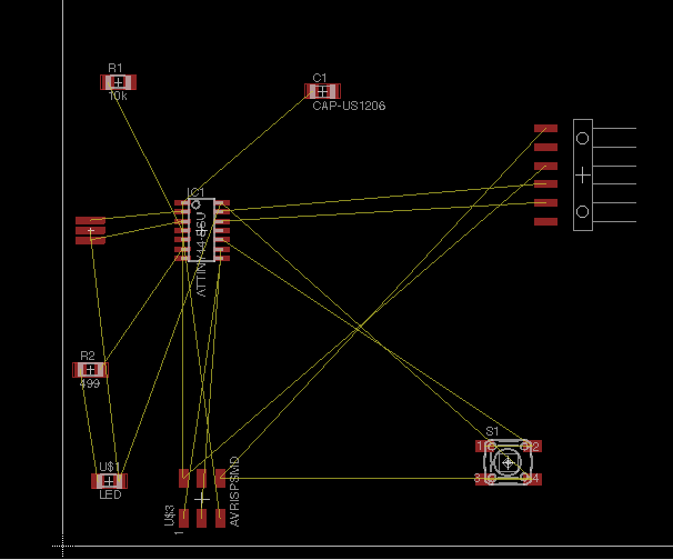
This cleaned up a lot of the mess so that I could actually see what was going on. I realized after the auto-router that the point of the yellow lines was to act as a guide to show which components would be connected and which should not be. When a component was correctly connected with a trace the yellow line went away.
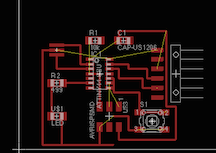
I then set out to use the manual rout to connect the components. It became immediately clear that there is a real art to positioning all the components so that that the traces connect without crossing. I made a lot of progress but I was a bit frustrated and confused by the fact that I could not get the last few connected and for reason I do not understand I could not get some of the yellow wires to disappear. Also equally concerning there appeared to be connections that should not be there.
3/4/2016
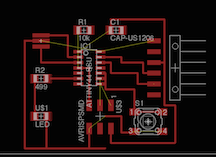
I started over many times and with the Auto-routes. It became clear that how the components are arranged has a huge impact on how Eagle routs the traces. Obviously it must tie into how it optimizes the path. Moving the components even a little up or down will totally change how it auto routs. After trial and error I finally managed to get it to auto-route all the traces. I decided to go with the auto-route that I had but then I realized that my board was in fact missing a connection between one of the pads on the jumper and the bottom pin on the ATTINY. I could not figure out why because when I looked at my schematic and it looked like it was exactly the same as the one I was basing my board on. Clearly one of the lines I labeled was not making a connection from my schematic. To test this I tried copying and pasting the entire schematic from the board I was trying to redraw. When I checked the connections the connection between the jumper and the ATTiny was there so that there is something wrong with my schematic and not something wrong with my Eagle settings. I decided I would need to redo my schematics as the best way to fix the problem. But I have hit my limit of 4 hours messing around with Eagle and so that will wait for another day.
3/5/2016
Actually my needing to start over worked out because I went through from the beginning with two of my lab partners who had not yet made their schematic. Happily when I redid it, all the connections were there. I learned several things. One small trick I learned that saved time was that when you are connecting two components you do not need to draw a line between them. You only need to touch the tips together that you want to connect and then you can pull them apart and they will have a green connection wire. As is the pattern, it took me three hours, at least, to make my first schematic, this time it only took me 45 minutes and that included helping two other people and as I said it actually worked this time.
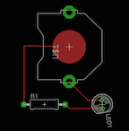
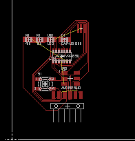
I arranged the components in the approximately the same pattern has I had the day before and I auto-routed the board. I got 100% of my connections the first time so figured I might as well go with it because it seemed as good as anything I would do. The only thing I changed was that in a few places it ran the traces underneath the resistor and LED. I knew enough that this seemed a bad idea. I broke the traces and turned them back into air-wires and then rerouted the traces around the resistor and the LED. Next I set my board to cut on the other mill.
Cutting the board on the Othermill
Previously we had cut out a board made from the sample schematic just to see if we could program it. The board was taken off the other mill before the actual outline of the board as cut so I had to cut the board with snips. This proved to be really difficult because the board cracked really easily. Most importantly I realized where the outside trace needed to be and I knew it would be wrong on the board I was cutting. I was not really thinking but when I made my trace I made it in relation to the white graphic of the jumper not the pads. Oh well it was too late to do anything about it, the Othermill was almost done.
I used solder paste to put down all the components. Having made the previous boards this was pretty easy. I first put solder paste on all of the pads and then on the pads for the resistors, capacitors and the LED. The only issue was it was not clear to me which way to put the LED. It had a green mark on the bottom. I found this website ( click here.) and it said the green side was the positive anode. I still did not know which way to face but the schematic seemed to indicate that the cathode went to ground and the anode faced the resistor. Next I put on the ATtiny, the button and the jumper.
This time rather than use the UV oven I just used the hot air gun to melt the solder paste. This worked really well and was much faster, it took me about two minutes to melt all of the solder paste. The only advantage I could see for the oven would be if you had a bunch of boards to do at once which would certainly fit a classroom situation.
We tried to program it but we got the same exact error message we got when we tried to program our FAB programmers from week 4. Oh well, should have expected as much.
3/7/2016
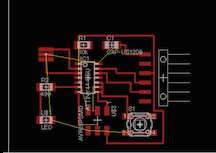
My board was messed up every which way possible. First the outline around the jumper was too far out. In addition there were several places where the othermill did not cut out traces when two traces ran side beside. I am learning an important lesson with digital design. It is really easy to design something digitally that far exceeds the ability of the device that will actually make it. Oh well, time to start over.
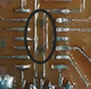
I kept my schematic and tried doing some more auto traces but it quickly became clear that it would be more work fixing all the places it messed up than it would be for me to make all the traces myself. I worked for several hours trying various routes for my traces. The biggest pain was getting the traces through the ATtiny. Eagle has this really annoying way of making traces in defined segments. In other words there is a minimum length that it will allow you to make a line. As a result when you try a line from the interior side of a pad on the ATtiny it either barely comes out in which case you are forced to run your line along the pads which will not be enough space. On the other hand if you pull the line out farther it moves to almost the center. This makes it really difficult to get multiple traces to run through the pads. In addition it snaps to particular parts of the pads. This makes it difficult to get the path you want. One other buggy part of Eagle is that once you have created a trace it leaves an airwire that sometimes can be difficult to get rid of without getting rid of more of your trace than you want.
I was forced to make some crazy paths to get what I wanted such as the two angled paths through the ATtiny.
What was somewhat hair pulling about doing it this time is that I was paranoid about having any traces to close. I probably overcompensated for a safety margin of lines but if it works I do not care. To view my eagle schemetic ( click here.) to see file for brd ( click here.)
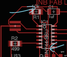
One thing I did not like about my previous design was that there were some places that traces were close to pads. This was pretty annoying because the lines seemed to snap to grid so it was really hard to get lines to pass exactly between pads. I finally realized that in the upper left corner there is an option to set the grid. I set the grid to 0.0001 which gave me the ability to get the lines spaced about better.
I was confident that I could get this board to work. One of the boards that I soldered using a sample design worked when David tried to program it.
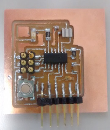
I milled out my the hello world I designed on Eagle cad. It looked pretty good but I would make my traces bigger next time. I was so paranoid about traces touching that I think I over compensated .
Soldering my Hello World board
I collected all the components for my helloworld board and soldered them using solder paste that I melted with a hot air gun.
After soldering my board I next test my board with a Multi meter. Oddly, when I was testing the various pins of the ATtiny44 I could make the LED light come on using pins that were not being used and thus had no connections. Sure enough when I took the ATTiny off there was solder paste underneath the chip that did not melt.
I guess what happened was that solder paste got underneath the chip and because it was covered by the chip it could not wick when I heated the pins. I used the heat gun to quickly melt solder paste. To be on the safe side I replaced the ATTiny44 with a new chip, this time using surface mounting to solder. In the future I will not use solder paste for the chip and just solder it.
I tested my board for shorts again with the multi-meter and could not find any. It is time to move onto programing it. The lesson that I learned from this was that getting your board to work basically comes down to solder technique. Bellow is one of two Hello world boards that I made.
Final thoughts on soldering boards
As tempting as solder paste is that it really causes more problems then it solves. Certainly it makes it easier to solder but it does not wick as well as solder wire. As I experienced with the solder under the chip, it has a tendency get in grooves at which point it is really hard to melt. So my recommendation with solder paste is that you should use a tiny amount, making sure to keep it on the pads. Then melt it with a hot air gun to set the pieces down. This will make it easier to then go back with solder wire and add sufficient solder to ensure a good connection. However, as you gain confidence I would stop using solder paste ASAP because ultimately you will have less problems with shorts using solder wire.