06/ electronics design
This week's task is to redraw the echo hello-world board and add at least one button and LED to it.
1. group assignment
2. electronics design
3. PCB fabrication
4. programming and test
← previous
→ next
⋯ assignment list
🏁/ final project
Group assignment
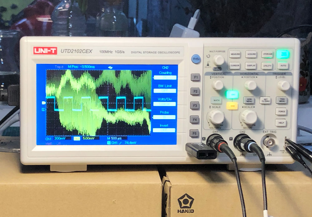
This week as a group we used the oscilloscope in our lab to see the signals of a resonator on a microcontroller circuit board, and multi-meter to test voltage, current, resistor value and continuity between components. Pamela has documentation on her page:
group assignment documentation link
It is cool to see the visualization of signals on an oscilloscope, and compare one type of signal to another at the same time. You can adjust the voltage and time unit to see the signal graphic at different scale. At current state, oscilloscope is an add-on because the board we are making now is simple and has few things to test, but multi-meter is the key to solve problems and it is important to know how to use it effectively.
Electronics design
To design the board, I use Autodesk Eagle for EDA (electronic design automation). I find this eagle tutorial very helpful. Here are the steps:
1. First create a new file and get a blank canvas in schematic view. A schematic is a drawing representing a circuit. It uses symbols to represent real-world electronic components. In schematic view we sort out the logic among components.
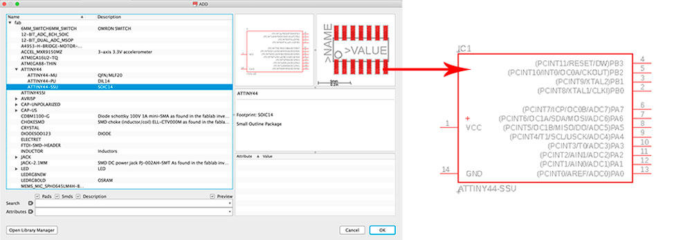
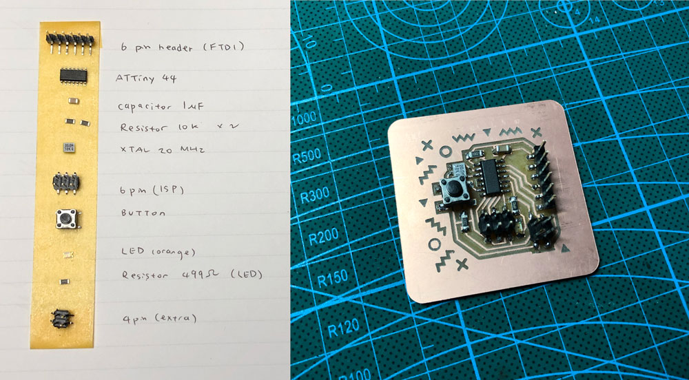
2. Add components by clicking the add button in the left tools bar and search for the name through the list. The components I need are:
- – microcontroller ATtiny44
- – crystal 20Mhz: external clock. The attiny has a 8Mhz clock but the resonator is faster (increase the clock speed of the processor) and more accurate.
- – capacitor 1uF
- – VCC and GND
- – button
- – pull up resistor 10Kohm for button and for RESET signal
- – LED and its current limiting resistor 499ohm
- – FTDI 6-pin header: powers the board and allows board to talk to computer
- – SPI 2x3 pin header: for programming the board
3. Install the Fab Lab components library (fab.lbr) which contains frequently used components in fab labs. By narrowing down the in-use library down to Fab library and basic supply1, you can find almost all the components you need for this assignment and save a lot of searching time.
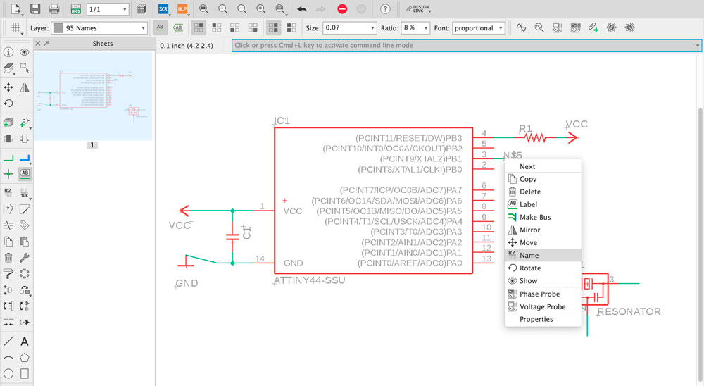
4. Notice the components we use for the board are the surface mounted types instead of through-hole. Once the component is placed onto the canvas, you can move it around and right click to rotate before you click again to set it to a fixed position. You can always move and rotate by finding the command icons from the tools bar.
1. First create a new file and get a blank canvas in schematic view. A schematic is a drawing representing a circuit. It uses symbols to represent real-world electronic components. In schematic view we sort out the logic among components.
2. Add components by clicking the add button in the left tools bar and search for the name through the list. The components I need are:
3. Install the Fab Lab components library (fab.lbr) which contains frequently used components in fab labs. By narrowing down the in-use library down to Fab library and basic supply1, you can find almost all the components you need for this assignment and save a lot of searching time.
4. Notice the components we use for the board are the surface mounted types instead of through-hole. Once the component is placed onto the canvas, you can move it around and right click to rotate before you click again to set it to a fixed position. You can always move and rotate by finding the command icons from the tools bar.
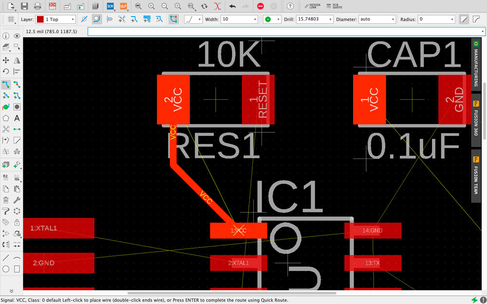
5. Connect the components by choosing net from tools bar and adding visible wire between components, or adding same name lables so they will get connected automatically. Use the ERC (Electrical Rules Check) to verify the design.
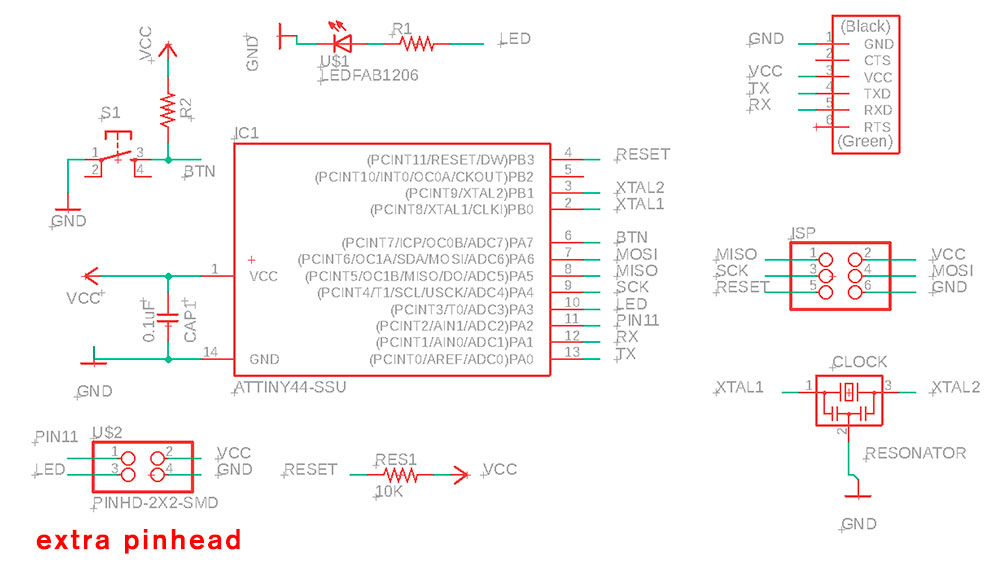
6. Here is the finished schematic view. I added an extra 2x2 pin header to extend the unused ATtiny44 leads, LED, VCC and GND.
7. You can also switch to the board view which simulates the layout of the PCB board. Drag components around to organize them.

8. Use route from tools bar to route each trace manually. You get more control this way than using auto-route.
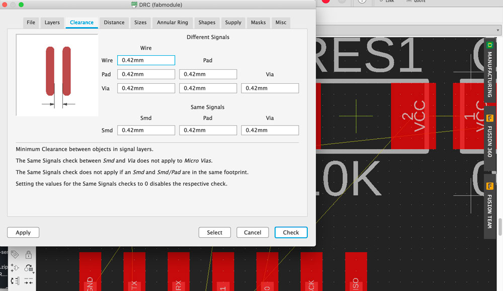
9. Download DRC (Design Rules Check) for fablab and replace the default one with this new one to make sure the space in-between routes is enough for the 1/64 endmill to cut through.
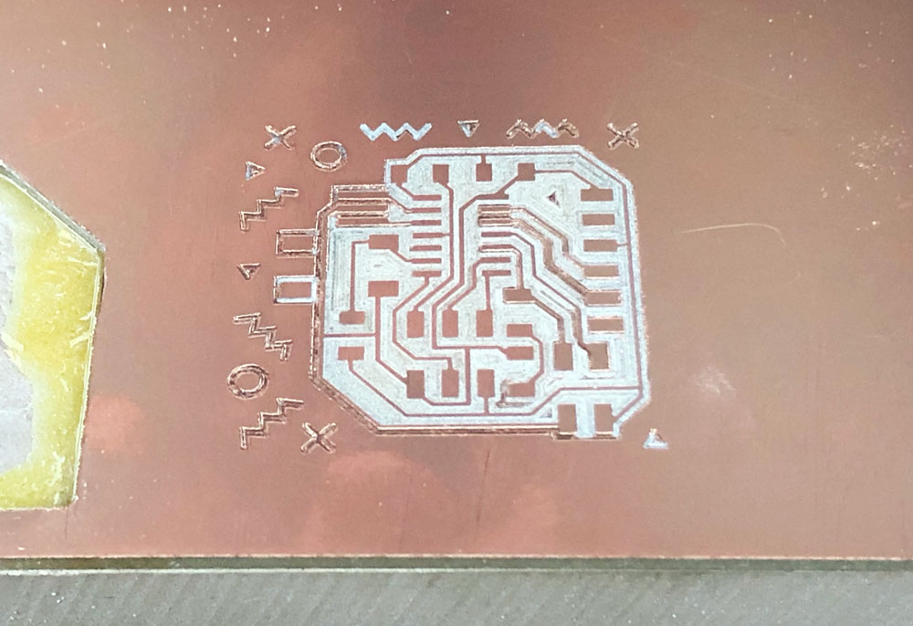
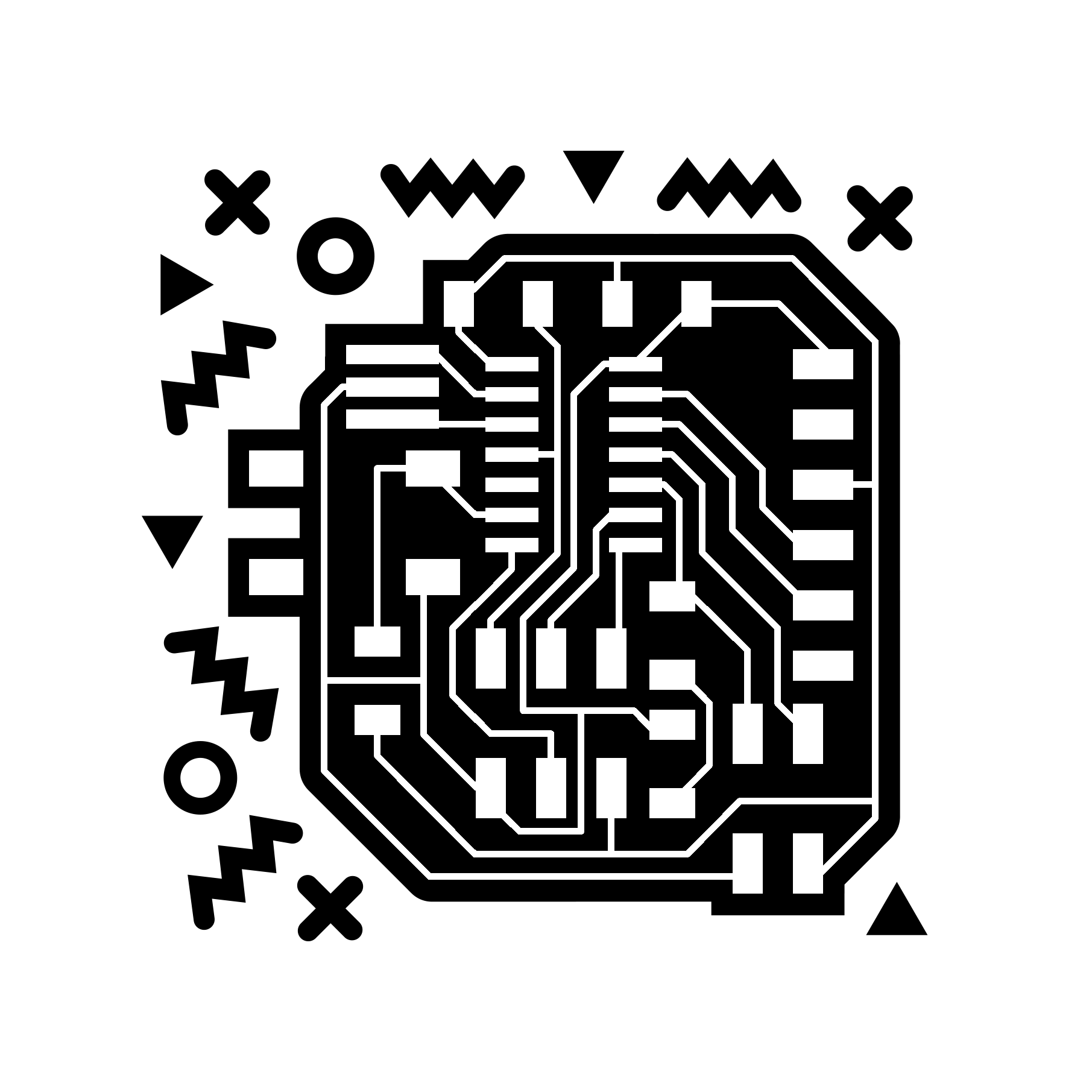
10. This is how my board looks like after I organize the routes. By turning of layers and uncheck the show-name boxes under setting I can remove the info I do not need from the board view and export the clean trace to .png file.
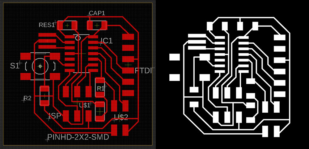
↓ download .png file: 06_echo_helloworld.png
↓ download eagle file: 06_echo_hw.sch, 06_echo_hw.brd
PCB fabrication
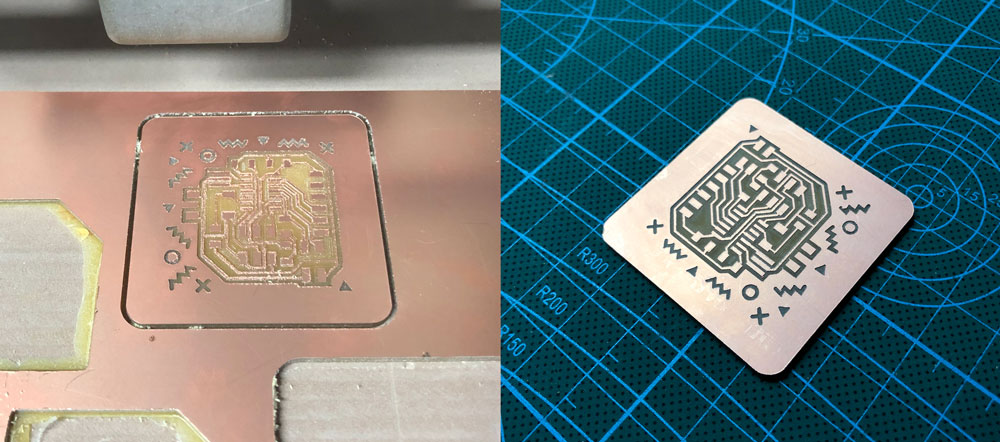
I added some graphics around the circuit design for decoration :D
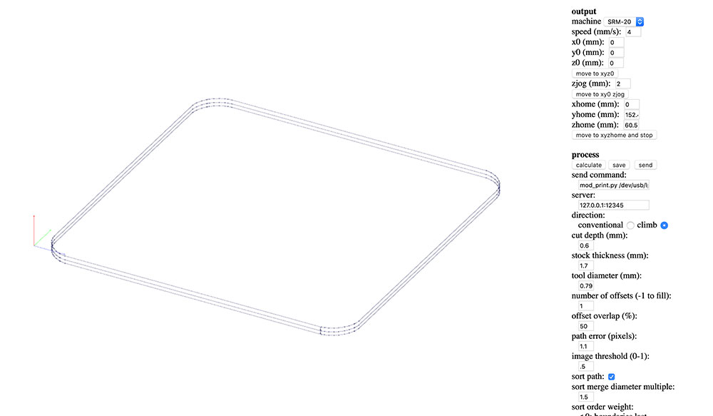
Then I went through the same process as I did for my FabISP from week04. The .png files got imported into Fab modules and exported as .rml files for milling.
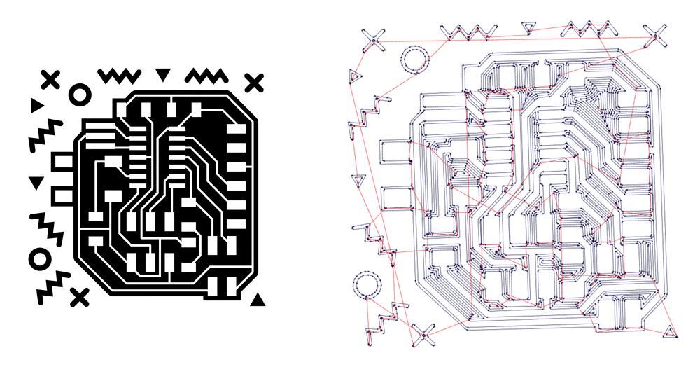
There is still some copper left between narrow traces that does not get cut out entirely. It is clear from the calculated trace view (above-right image) that one single-time outline route is not enough to cut out the material in-between.
So I thickened the outline for the circuit part, the graphics, and milled again on the previous one. The bold traces turned out better but it was still not 100% clean between some narrow traces.
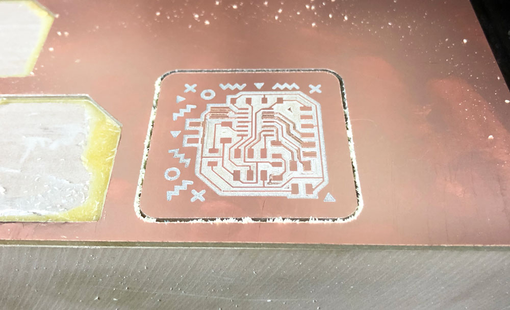
I modified the .png design again to add more space around because I came up with the idea of inserting the PCB into a case or a frame as part of the design.

↓ download .png files: 06_helloworld_f_trace.png, 06_helloworld_f_outline.png

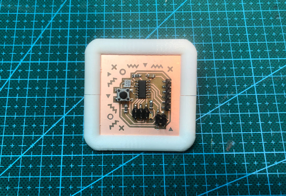
The milling went well. I arranged the physical components and soldered them onto the board.
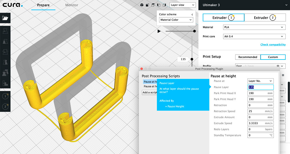
Then I modelled a frame in Rhino, sliced it with cura and printed it out.
Now my PCB is happy with a frame :D
Programming and test
The next step is to program the board and make it alive. I follow this workflow for hello.ftdi.44.program.

1. Connect the FabISP to computer, 2x3 pin header on FabISP and the new PCB accordingly, and 6-pin header on new PCB to external power with an FTDI cable.
2. Download the hello.ftdi.44.echo.c and hello.ftdi.44.echo.c.make file from embedded programming week page. Save both file into the same folder. Do not open either file with any application. Rename the .make file to Makefile with no extension, and leave the .c file as it is.
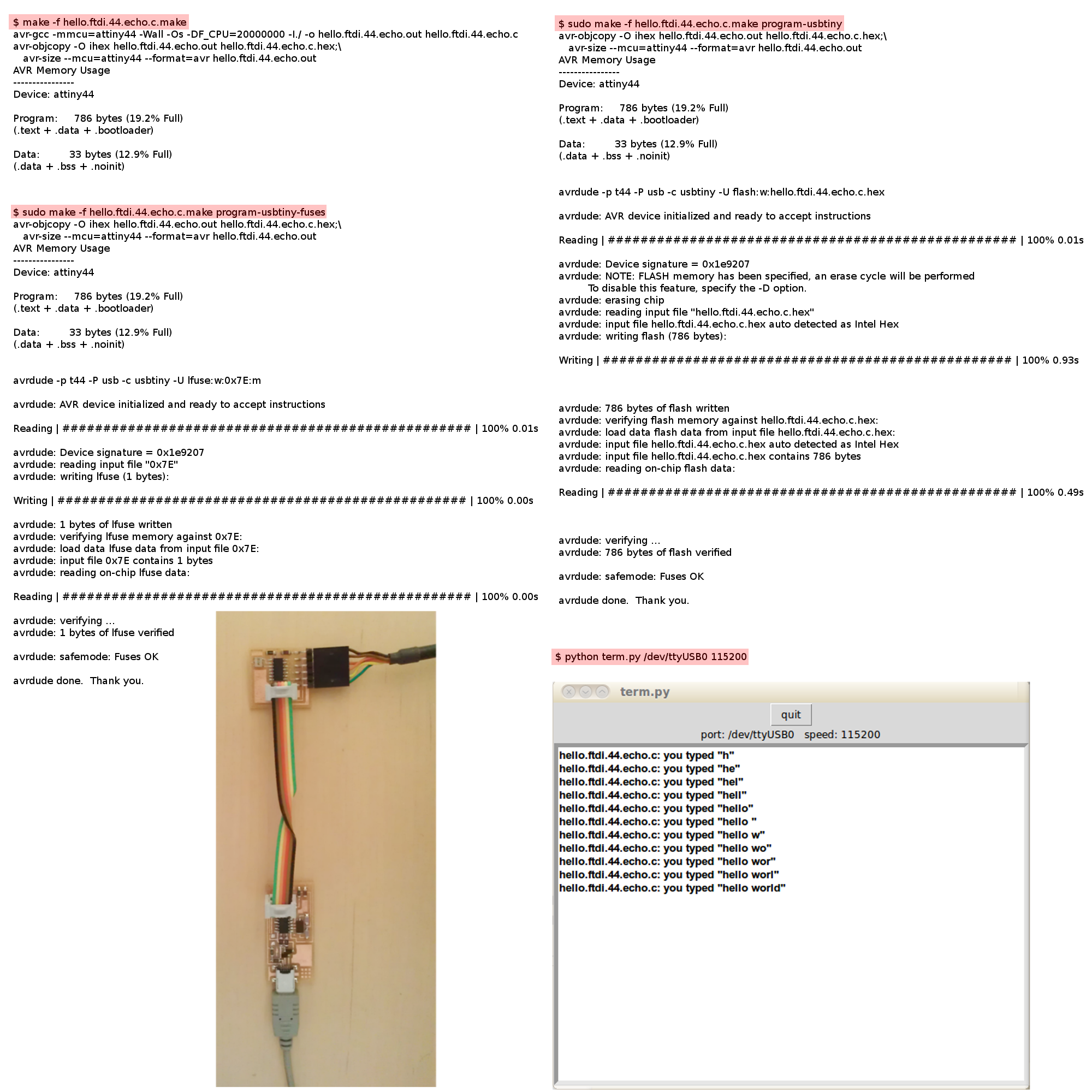
3. In terminal on Mac, cd to the folder with makefiles. Run these three commands one by one:
make
make program-usbtiny
make program-usbtiny-fuses
If you see a lot of bars it probably means it is working. If there is any error message, double check the connection, cable, switch to other FabISP or computers and test.
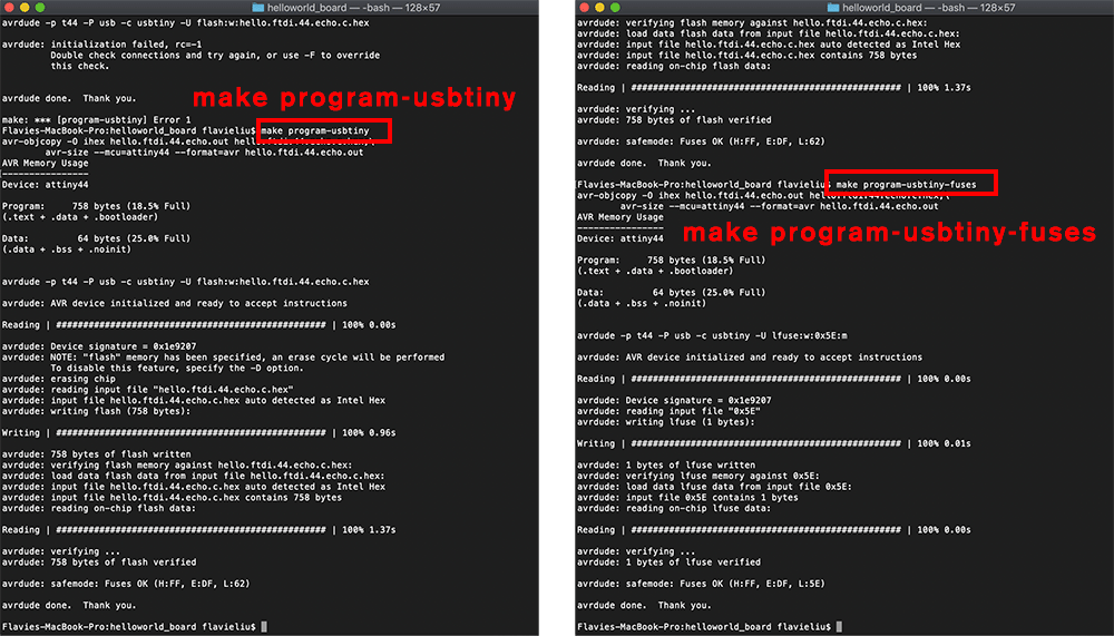
I had error message suggesting "cannot initialize, check connection" for a long while :'( With the help of my local instructor, I figured out that the problem was bad soldering connecting one pin header to a nearby trace causing a shortcut.
We later discovered another bad connection that the Tx leg from ATTiny44 was not touching the ground so it could not transmit with FTDI pins. It was very useful to check with multi-meter.


After the board is programmed, I can take away the FabISP and connect it directly with my computer using the FTDI cable. Now I want to test if the board can echo in arduino.
1. In Arduino, add the ATtiny board by open preference, copy and paste the URL below in and then select the new library from the board manager.
https://raw.githubusercontent.com/damellis/attiny/ide-1.6.x-boards-manager/package_damellis_attiny_index.json
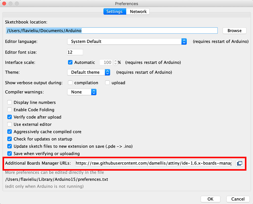
2. Under Board>Boards Manager, install the attiny by David A. Mellis.
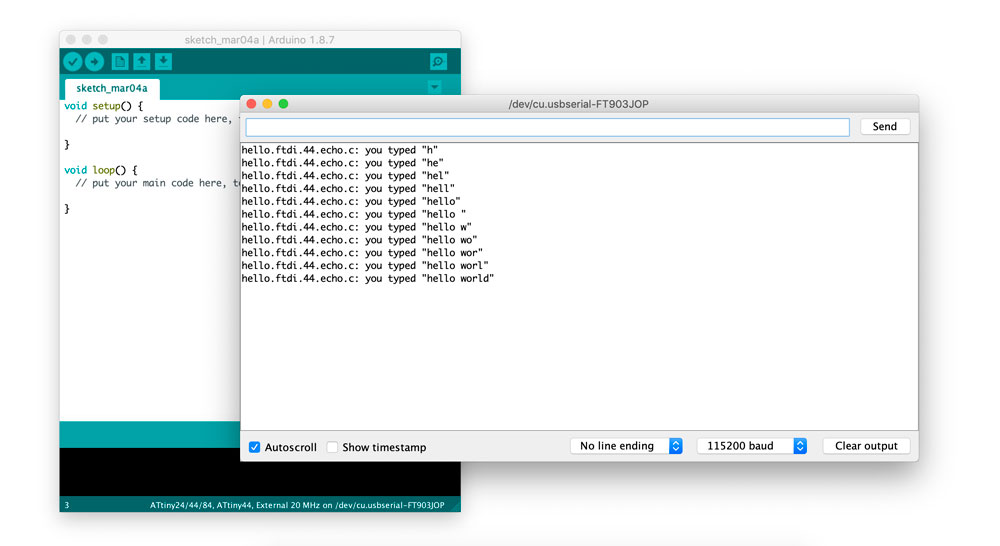
3. Download and install the FTDI driver for the cable to show up in Port.
4. Under Tools, select Board: ATtiny 24/44/84, Processor: ATtiny44, Clock: External 20 Mhz, and Port: dev/cu.usbserial-... (other than the bluetooth one)
5. Restart Arduino if you cannot see the options. It usually works.
6. Open Serial Monitor, choose No line ending, test and pick a communiction speed (in my case 115200 baud) and start typing.
It echoes! Hello World :D
(Updated 03.05.2019)