Designing the board
We prepared for this week's assignments together as a group, with the help of this week's instructor Antti Mäntyniemi. We all downloaded and installed the same program to redesign our own Hello-World board. The software is from Autodesk and called Eagle.
Before opening up eagle, we saved a few files to our computers from the interwebs. The first one was the fablibrary that included some components specifications we wanted to use
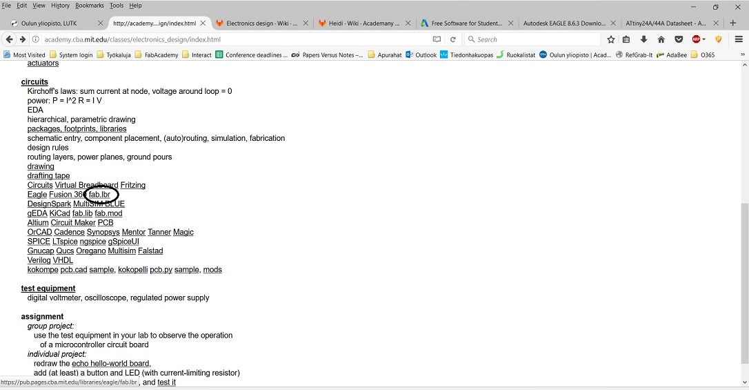
Next we downloaded Neil's hello world board for reference


As well as the Attiny44 datasheet.

Then we proceeded to open up Eagle, clicked on file-->new project and named it. I named mine just the hello world board
Next we chose this new project from a project tree on the left, rightclicked on top of it and chose --> new schematic.

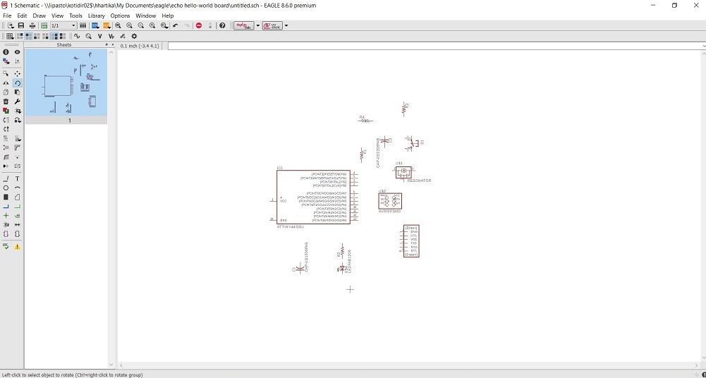
This is the starting point of our project, a blank schema where we will now start to add components into, and link them together.

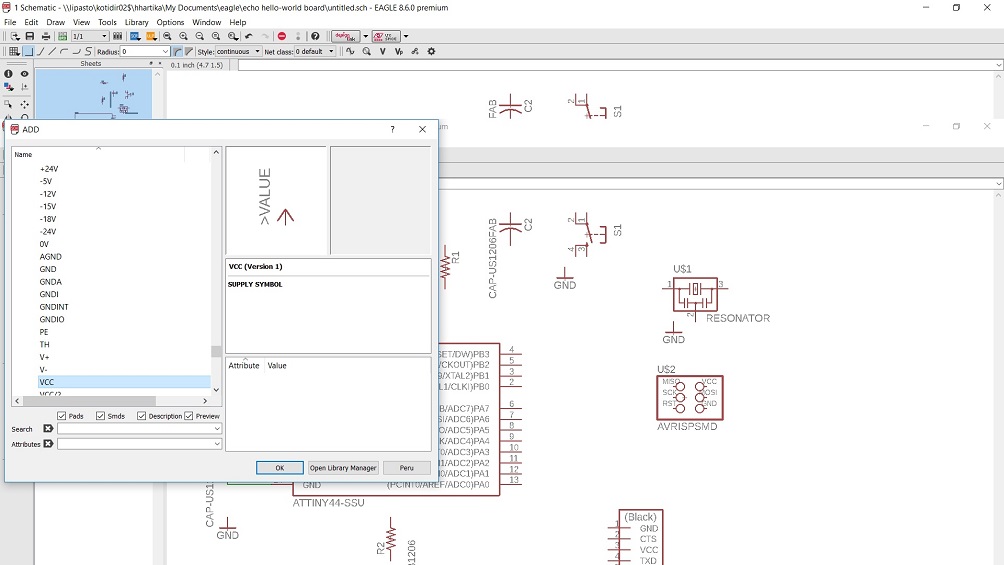
The first thing that we added was the fablib file that we downloaded into our computers. We browsed into the folder where it was located and clicked add.

Then we started picking components from that library (and others) that were specified in Neils board into our hello -world schema.
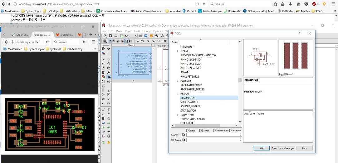
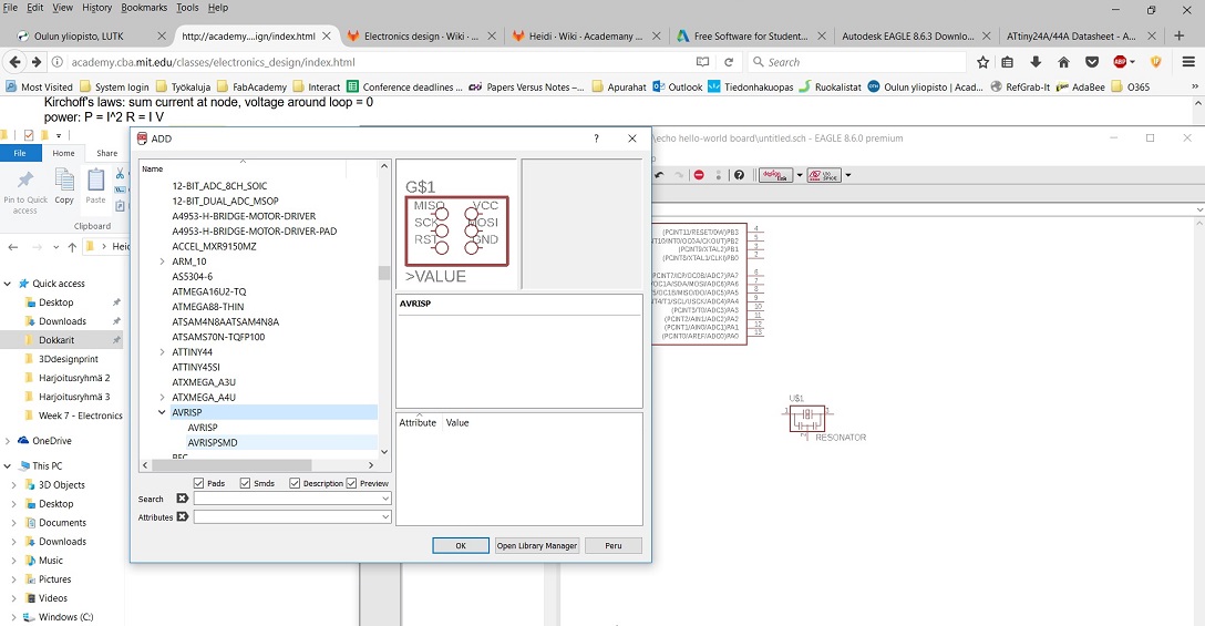
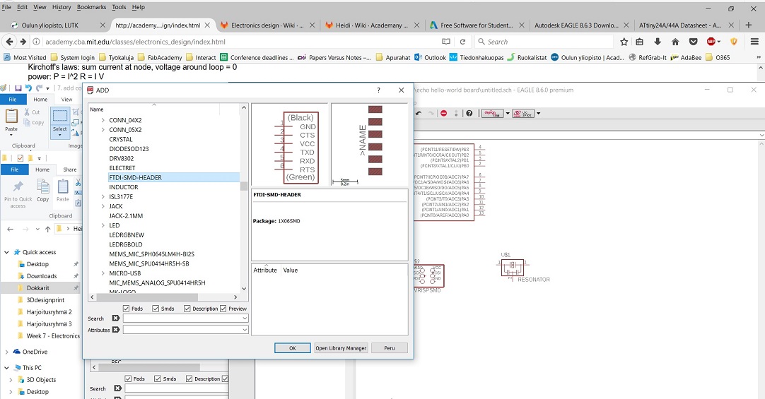
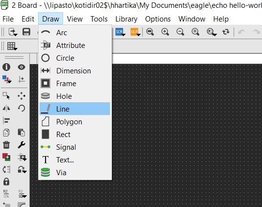
The first thing we added was the ATTiny 44. We clicked on "add component" button from the tools menu on the left, navigated to the fab library, and browsed for the correct component as shown below.

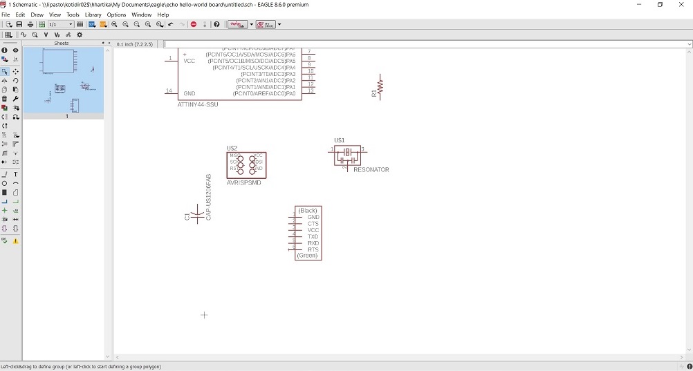
Then we added a resonator.
And an AVR ISP connector
Next we put an and FTDI-SMD header (I have no idea what it is, mind you)
a capacitor.
_more room under the resistor.jpg)
and resistor
_more room under the resistor.jpg)
And that concluded gathering all of the necessary needed parts for our Hello-World board.
However, in this week's assignment it was specified that we need to also add some additional components, at least a led, and a button.
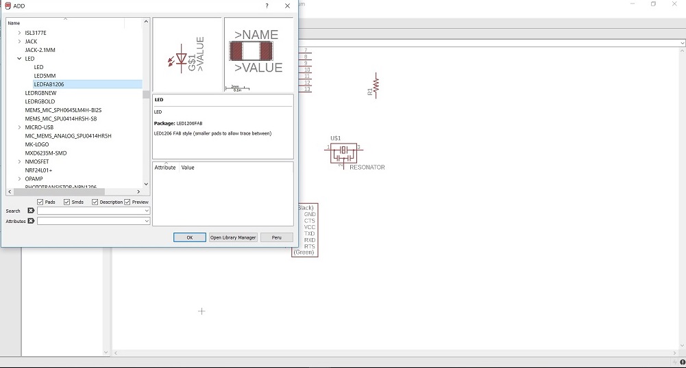
So --> We inserted a led
And used to copy tool to copy a resistor for it.

Next we added the button

And copied a capacitor and resistor next to the button
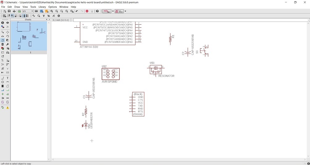
Now, finally, all needed parts were there.
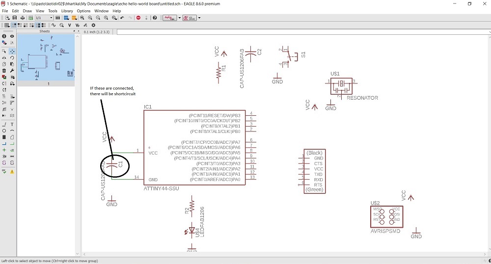
We started to use the net tool, and connected all of the components according to Antti's instructions

We moved capacitator 1 next to ATTiny44, and connected the capacitor to ground, and to vcc pins in the at tiny.

Next we started to add the ground and vcc connections to all of the components that needed them
We added ground for the capacitor

And we added vcc to the capacitor
And we continued to move this way:
We added Ground and VCC connections to the FTDI-SMD header, to the resonator, to the AVR ISP Connector and the button. To the led we added just ground.
Next we proceeded with the netting, with a word of warning - when drawing the lines, we should always be careful not to extend the lines inside and over the gap in the capacitor drawing. If the two sides are connected, it could cause a shortcircuit.
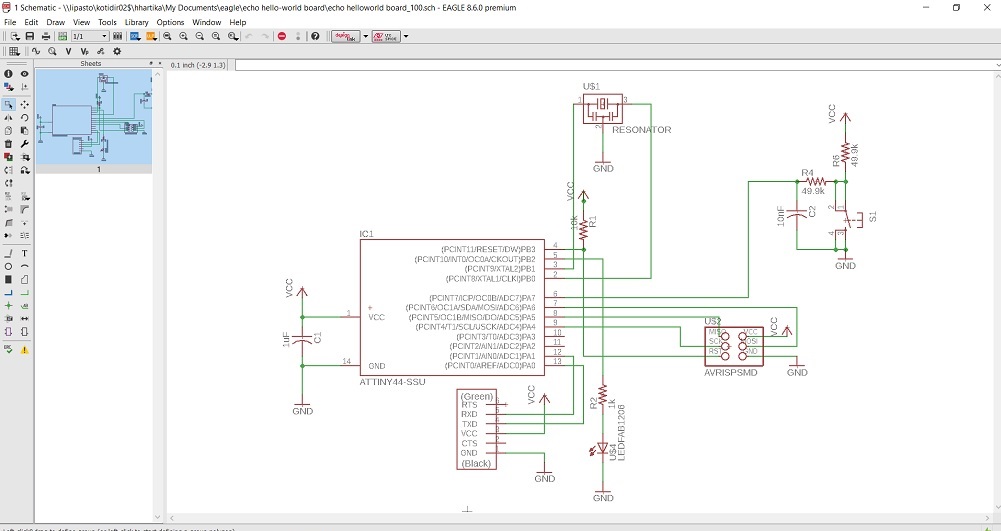
Here is a picture of the finished schema, with all of the necessary connections.
When we were ready with the connections and values, it was time to change to board layout from the menu in the top

On the left you have your components all connected. On the right you have your board. You just drag and drop your components where you want them.
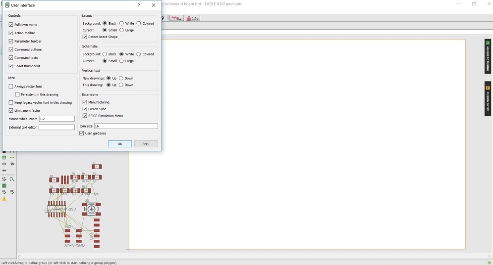
Before doing any of that, we however changed the board colour to black by clicking Options --> User interface from the tops menu and modifying the layout background colour. That is what all the cool kids are doing now. I guess there is some point to it? Perhaps it is easier to see the lines and connections you will draw?
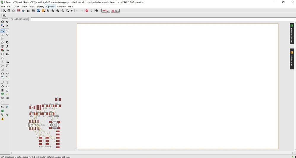
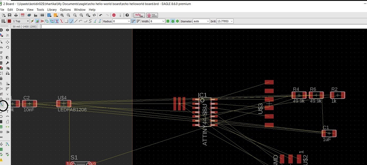
Anyways, I started to move the components to the board, on the lower left corner, quite close to each other
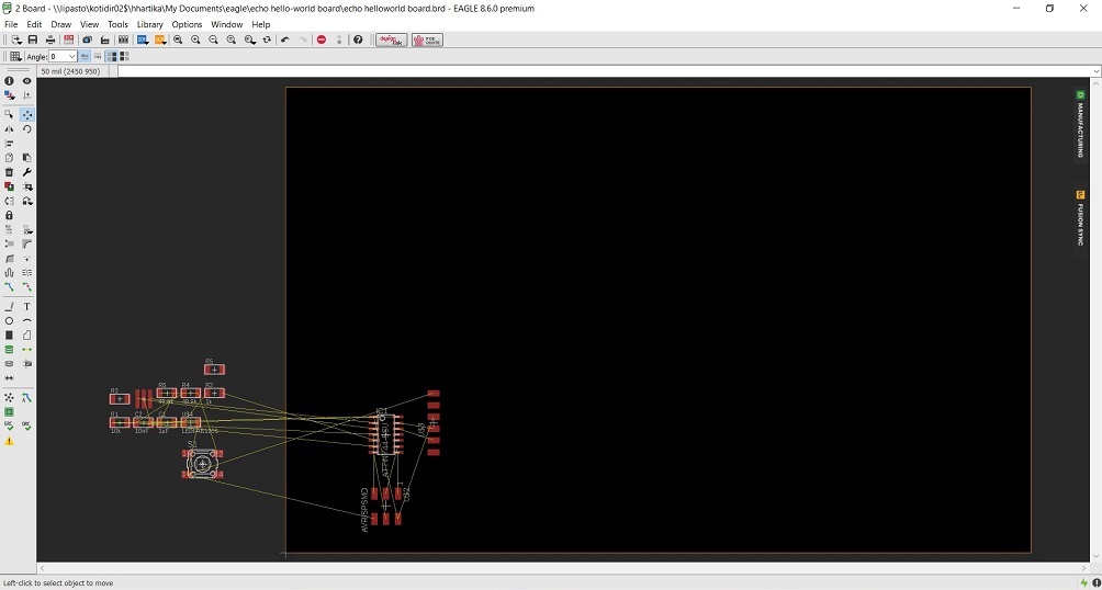
You might be doing this quite a bit, organizing and reorganizing again. When doing this, it is useful to press the "ratsnest"-tool every once in a while. It optimizes the wires for you.
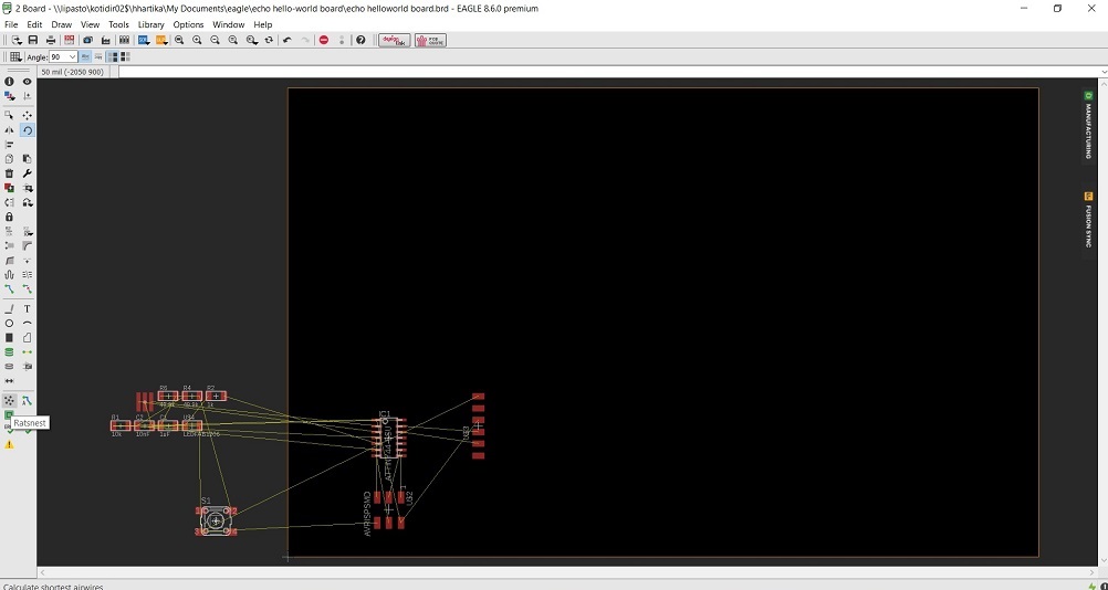
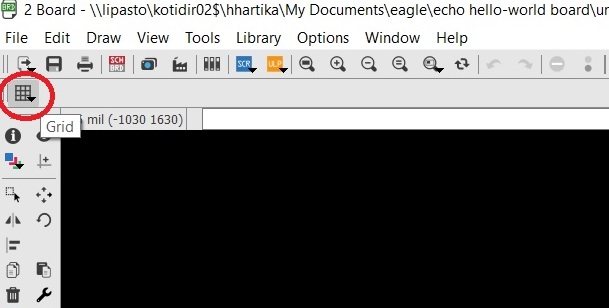
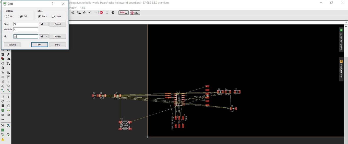
Another useful tool is the "grid". It draws you a help grid as dense as you want it to help you position your components symmetrically and to draw lines
When you have positioned some components and would like to start drawing a route for the milling machine, you use a tool called "route"
We set the route width to 16, so that it will not be too thin.

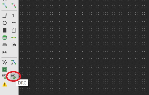
We also did some changes to other design rules that can be found behind the drc (design rule check?) button on the left hand side menu
We changed all clearance setting widths to 16 mil. I believe this means that between all lines we draw, there must be atleast 16 mils of space.
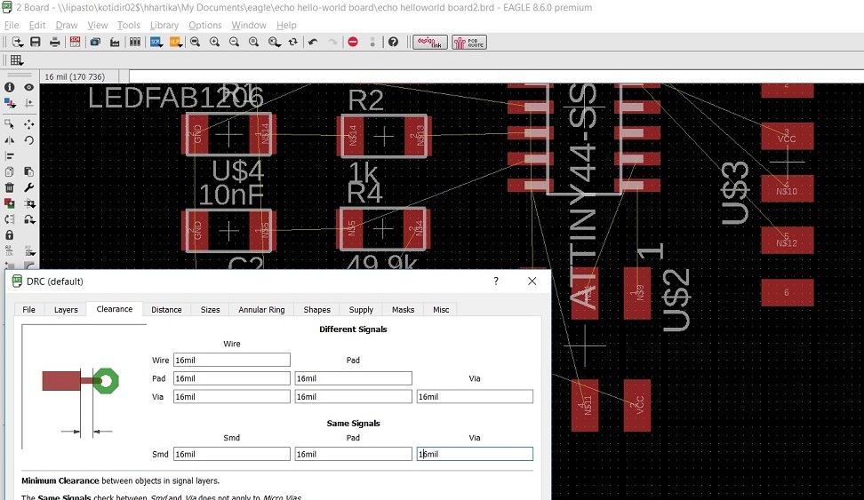
We also changed from here that the line size must always be 16 mil

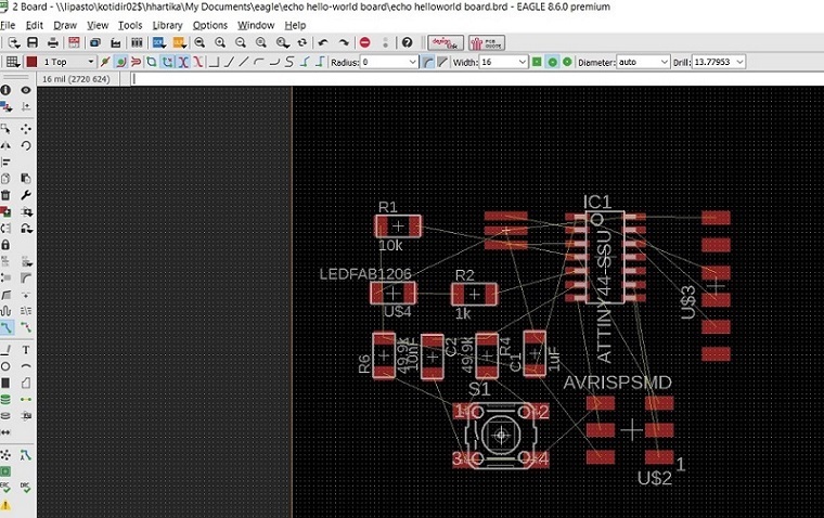
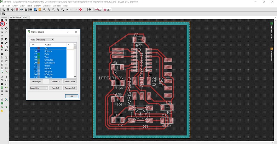
This was my draft one positioning the components.
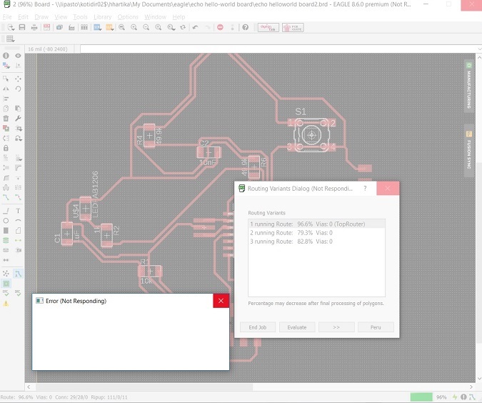
Now, at this point, I was supposed to use the "route" tool I showed before to start drawing lines between components, but what on earth did I find here? An autorouter tool.
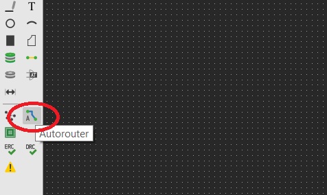
Autorouter draws the lines for you, using some fancy computer logic, that I of course thought would be better than mine. I spent hours that day rearranging all of my components over and over, using the ratsnest tool, and autorouting. Never to achieve 100% success. The highest I got was 96.6%. There was always some routes that could not be drawn, like in the picture below. Super frustrated.
When I went home that evening, I decided to give the board another go, but the program jammed and crashed on me.
When I managed to open it up again, i moved a couple of bits and pieces again, and tried the autoroute. Lo and behold it worked!
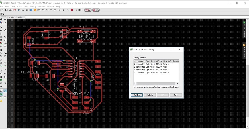
I did a couple of tries and all of them seemed to be working. I was a bit suspicious, but decided to enjoy it.
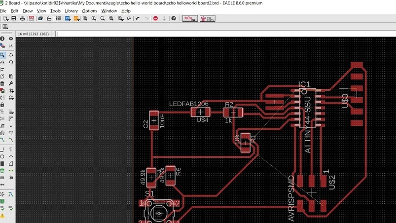
Of course it turns out my jot was premature. I did not realize that the blue lines in the picture meant that they go on the other side of the board (the board would be 2 sided.) Apparently when the program crashed, some settings were lost. When Antti explained this to me the next day, it was back to the drawing board. And this time, drawing the routes by hand.
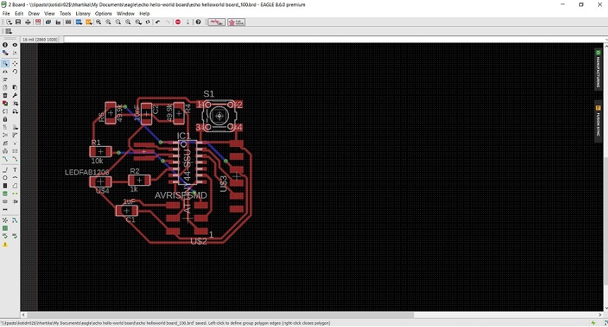
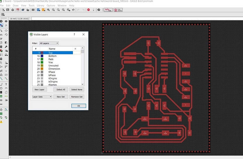
Turns out, this is much faster. I think it was less than an hour, and I had this drawn. It is not very eloquent, but it worked. When we did the "DRC" chack, there were only a couple of air wires, which were caused by the fact that when I had drawn the routes, I had not maneged to connect them all the way
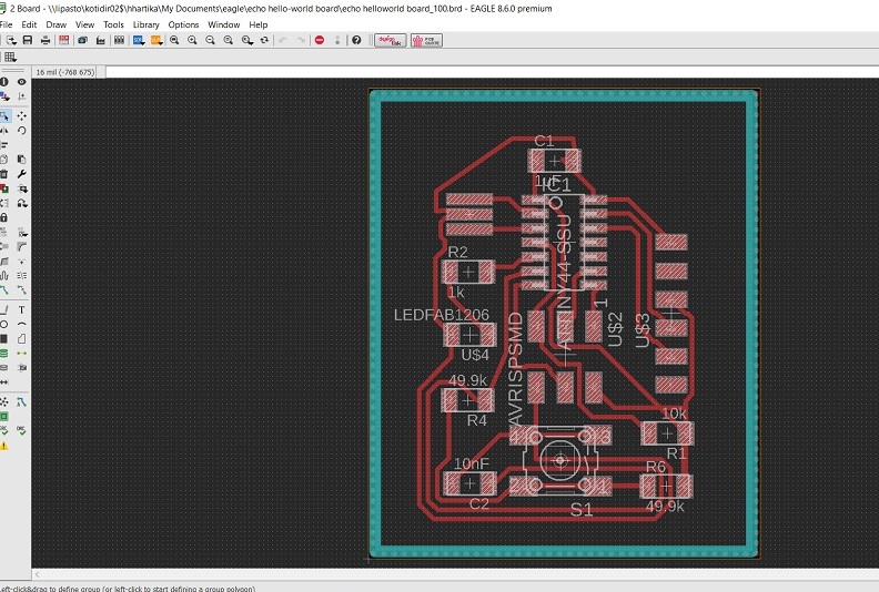
In the photo above I have already resized the board to be a little smaller just by dragging and dropping the corners. I have also added the milling lines to cut out the PCB like this:
First, select layers --> Milling. So that you are drawing on the right layer.
.jpg)
I selected "draw"--> "Line" from the menu above.
Choose layer 46 (milling)
choose to make a continuous line
2.jpg)
Make sure that the line is inside the yellow line so that it cuts
3_make sure it is inside the yellow line.jpg)
Heidi's Note: Now I know that before that blue continuous milling line, we also drew a dotted red line on the top layer underneath it. I can not for the life of me remember why though? Should have probably screencapped that thing, but of course was way too excited to finish.... Edit 16.3: Learned from my local instructor Antti that the dotted line was for the ground plane. It was done using Draw --> Polygon. Then select the polygon, choose properties, name it GND and, and use the ratsnest again which automatically generates it!
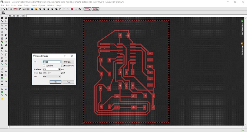
Next thing we had to was export the board in two image files:
A traces file that includes the routing for the mill, and
An outline file that includes the outline for the mill to cut out.
to do this, we used the layer tool from the left hand side menu
When you select the top layer, it will show you the traces.
Select export image

Name your file and save it as monocrome
Next choose layer again, this time the milling layer for the outline of the board.

Repeat the steps that you did for the traces file: Export image --> choose monochrome.
Files
- My hello world schema
- My hello world board
- My traces file for milling
- My outline file for milling
Milling the board
Milling the board was something that we already learned during week 5 of Fabacademy, so I proceeded to look at my own documentation from that week when preparing to mill my board.
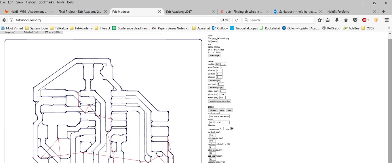
I went to fabModules website to work on the traces and outline .png files, to include your own milling machine specifications so that the board comes out right.
First I imported my traces file,
- I selected the input format to be png.
- I selected the output format to be for Roland Mill (rml), which is the brand of milling machines that we have at FabLab Oulu.
- I specified the I am doing a PCB traces
- I selected what Roland Mill machine I am using - It is SRM-20. When I select this, the FabModules gives me some default settings for the machine.
However, as different machines have different settings, mill heads etc. I then proceeded to modify those settings according to what our local instructor advised us.
- I changed the x,y and z values from 10mm to 0mm.
- I also did some slight modification to the process settings this time, according to what Antti advised me. I used cut depth 0.11mm and tool diameter 0.38mm (when I did my first board I used cut depth 0.1mm and tool diameter 0.4mm which also turned out fine).
--> I proceeded to press calculate, and got the following result that shows me milling lines and offsets. I saved it to my computer as a .rml file
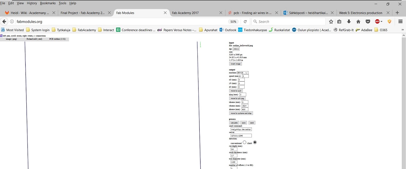
Next it was time to start working on the outline file.
- I again defined that the input file is image (png)
- I then defined that the output format will be Roland mill (rml).
- I specified that this time I am doinf PCB outline.
- I selected the output machine to be the SRM-20 again, and changed x,y and z values from 10mm to 0mm.
- I also did some modification to the process settings: Tool diameter was changed to 1.015mm, cut depth was set to 0.6mm.
--> Pressing calculate gives me a picture that shows me milling lines and offsets. I saved it to my computer as a .rml file
Files
- My hello world traces rml file
- My hello world outline rml file
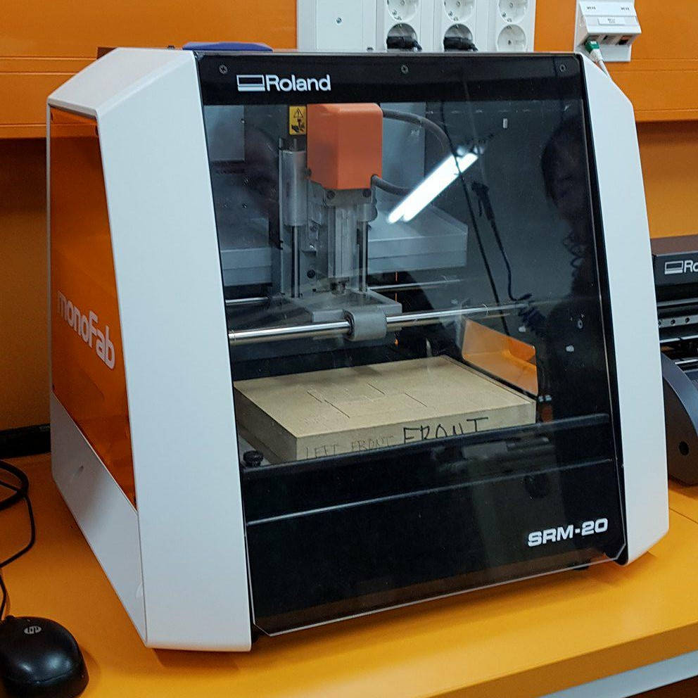
I took my rml trace and outline files and headed towards the milling machine and the computer that it is controlled with. Here is the Roland Mill SRM-20 that is used in FabLab Oulu.
- I removed the inner baseplate from the machine
- I took a fresh copper plate that I will be milling my hello world PCB into, placed double sided tape on it's bottom, and secured it on the baseplate.
- I put the baselate back in the machine and secured it to place, and closed the lid of the machine
- I put in the milling head to the milling machine with the help of the allen key
Next I started to work on the computer.
- I opened up the application that you use to control the machine. the UI of the Roland Mill at FabLab Oulu is called VPanel for SRM-20.
- I used the XY movement keys to move the milling head to the front left corner of the copper plate, and then hit the X/Y button (9) to set the origin.
- I used the Z movement keys to lover the milling head close to the copper plate, then used the allen key, loosen the milling head so that it touches the copper plate, and then tighten it back on. Then used the Z movement keys to lift it a bit from the plate and then hit the Z button to set the Z position of to the base point.
--> Once I got the coordinates fixed, I pressed cut, cleared the cutting queue by pressing "delete all", and uploaded my own traces file there. I press the output button to send my file to the machine to be milled.
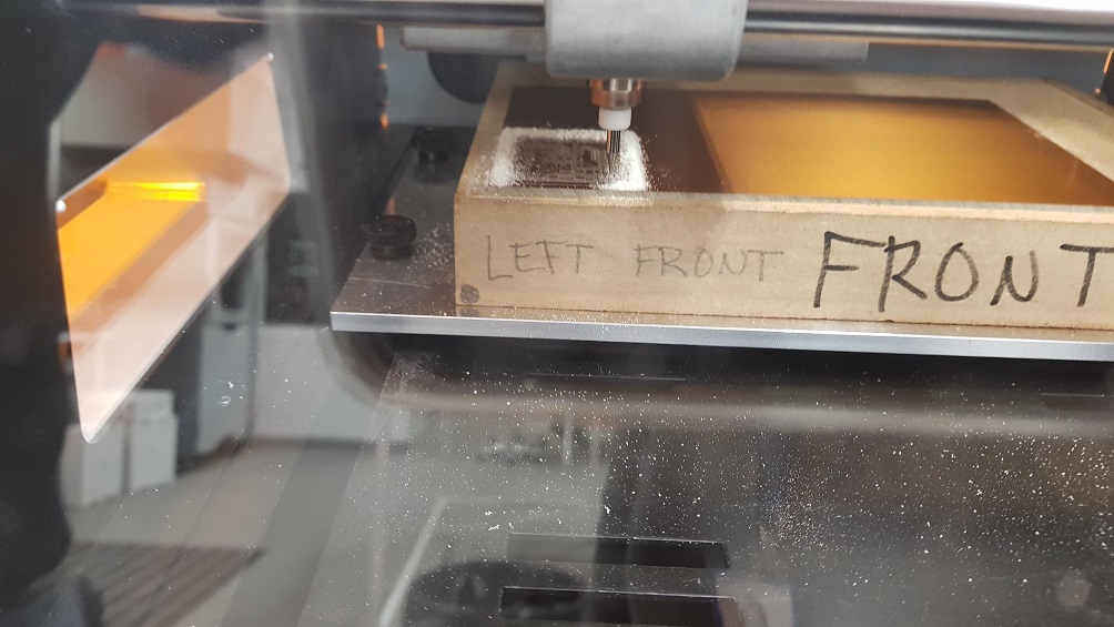
A couple of photos of my traces being milled


- When the traces were milled, I vacuumed the board (without removing it from the machine), and set out to cut the board out of the copper plate.
- First I changed the proper milling head to the machine. We used the flat headed 0.8mm tool. Then I repeated the some of the steps described above for the outline file:
- I used the Z movement tool to lover the milling head close to the copper plate, then used the allen key, loosen the milling head so that it touches the copper plate, and then tighten it back on. Then used the Z movement keys to lift it a bit from the plate and then hit the Z button to set the Z position of to the base point.
--> once I got the coordinates fixed I pressed cut, and a dialoque window opened up. I cleared the cutting queue by pressing "delete all", and uploaded my own outline file there. Next I pressed the output button to my file to the machine to be milled.
A couple of photos of my outline being milled

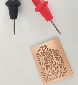
Once the outline was cut, I vacuumed the board again, and carefully removed my PCB from the machine. (As there usable copper board still left, I left it attached to the baseplate). After removing the PCB from the machine, I rubbed it with steel wool.
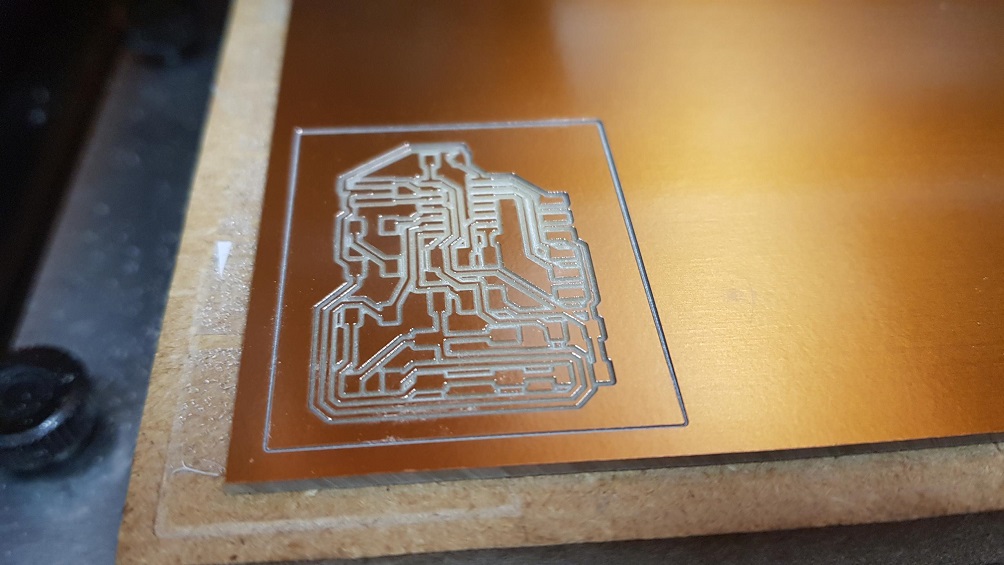

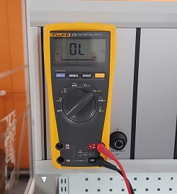
To me, my board seemed to look ok, but our local instructors were a little worried as some lines on the top of the board seemed a bit thinner than others. They explained that this might be due for example me attaching the copper plate to the machine in a way that is not secure enough. Because of this, after rubbing the PCB, we checked the board with a multimeter - if everything works/conducts just fine. Thankfully everything worked.
Soldering the board
Before assembling the board I printed out a component list from Eagle (export-->partlist).

I went to our treasure room to scour all the components needed, and placed them in a sheet of paper with explanations about what each component is. That way they were easy to tell apart when starting to solder. In the picture below, you can see that sheet of paper in the background.
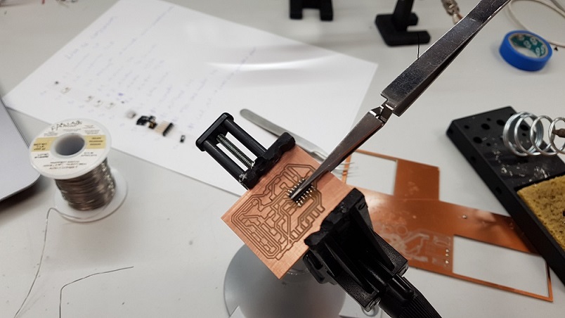
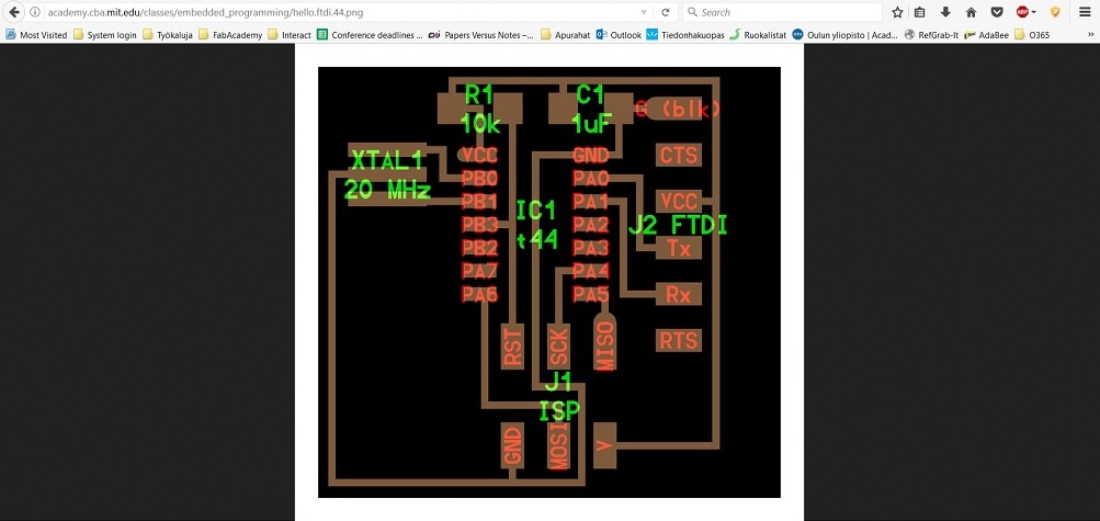
I also kept my computer open during the soldering process and had the following picture open on it, so I could check where everything goes.
Here are a couple of pictures from the soldering process:


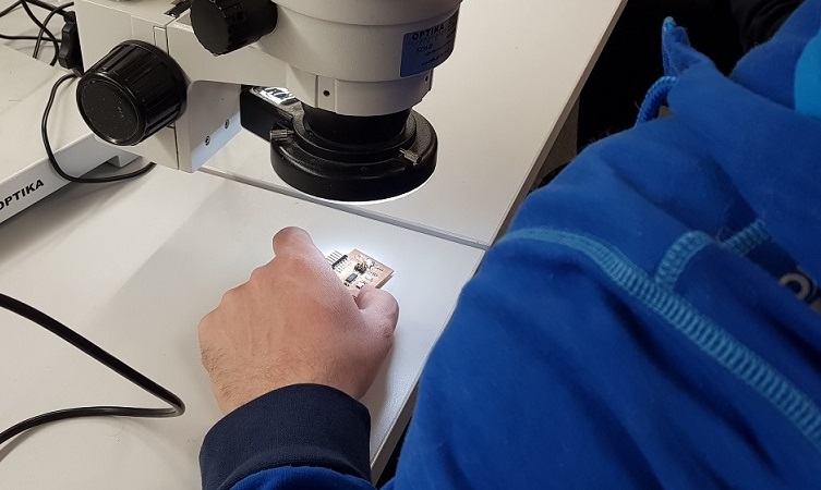
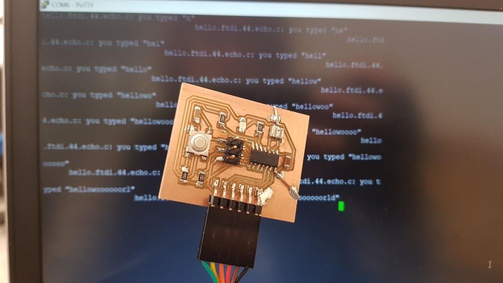
Once the board was finished, the result was checked under a microscope, and again checked with a multimeter.
Everything seemed to be in order, so it was time to move to the testing phase
Testing the board
I used these instructions to program my board. For this part I needed the ATTiny programmer that I assembled on week 5, an ISP cable to connect the the programmer to the new board, and a USB/ftdi cable (5V) to connect the new board to the computer. I also dowloaded the code and the make file needed
- When starting to program my board, I first opened GIT bash, and navigated to the folder where I had stored my code and makefiles.
- I then connected the programmer to the new board with an ISP cable, making sure that the ground pins are connected (blue wire)
- I then connected the new board to the computer with the USB/Ftdi cable which got the red light to light up in my programmer. Here I also made sure that the black wire is on ground pin
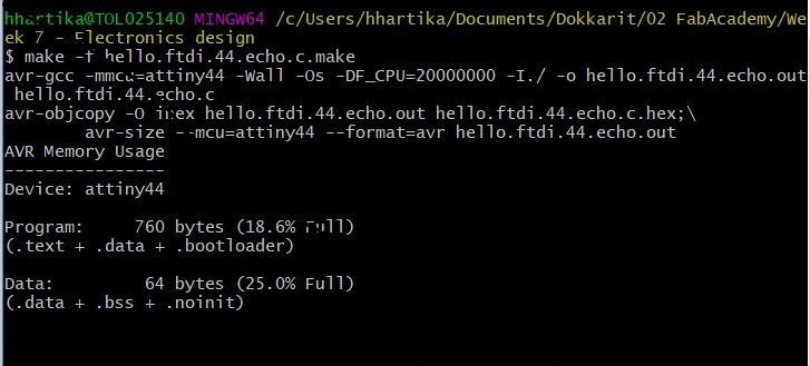
First I used the command "make -f hello.ftdi.44.echo.c.make" to make a .hex file for flashing
After that, I however ran into problems, that I have not been able to fix myself. I tried to run the make fuses command: "make -f hello.ftdi.44.echo.c.make program-usbtiny-fuses", but I keep getting errors
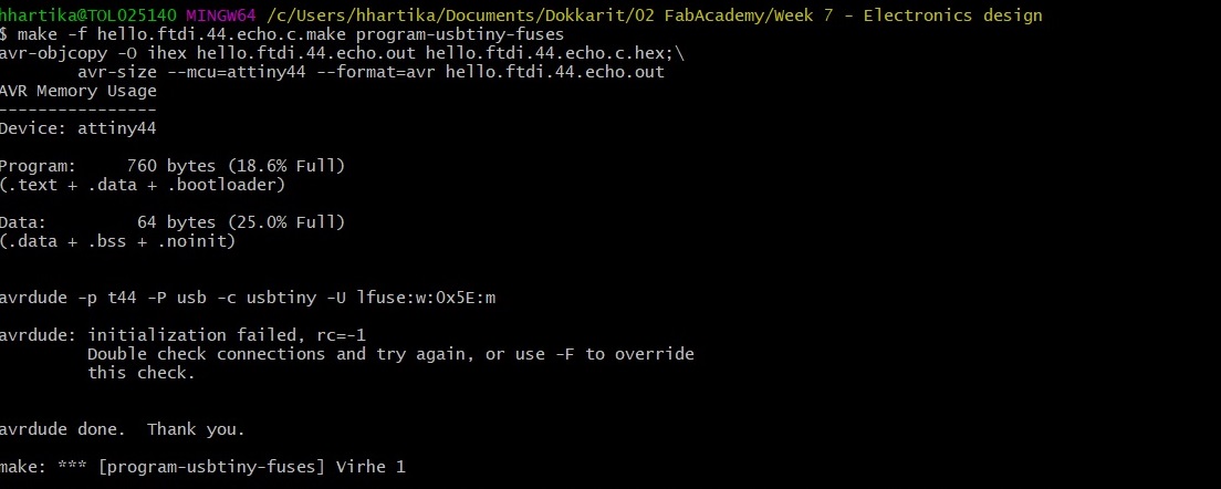
To solve this, I tried to
- check if the ISP cable is on backwards in the new board. I tried turning it around, but got the same error. The only difference I saw, was that the LED light in the programmer turned brighter.
- check if the ftdi cable is on backwards in the new board. I turned it around, but got the same error.
- check if the my ISP cable is faulty. I borrowed a friends cable, but got the same error.
- Megumi tipped me of this post from a previous year student, discussing the same error. Following their advice I have downloaded and installed VCP drivers for win 64 bit, which did not help. (I later learned that this was not needed for the cable we used)
As I was not unable to solve the problem on my own, I turned to this week's instructor Antti for advice.
- He checked if either my programmer or my hello world board had short circuited. This did not seem to be the case)
- He checked the soldering of my board, which seemed to be in order. Just in case he strenghtened the earth connections in some places with more tin.
- He used his own programmer to program my hello world board which worked just fine. So here we were able to isolate the problem to my programmer.
Solution --> I soldered the jumper back on, reprogrammed my programmer using Antti's board following the instructions on week 5.

After reprogramming my programmer I tried again
I attached my programmer to my my hello world board and both to the computer.
I ran makefuses

And make hello world

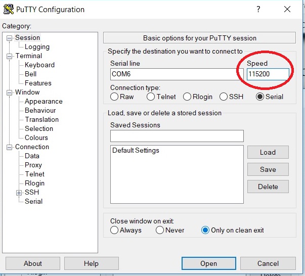
Then I took out my programmer from the loop, and checked the port the HelloWorld board was attached to from Device manager on my computer. It was Com6

I opened Putty, selected connection type Serial and added Com6 as the port. Here I made the mistake of not switching the speed setting, I was not aware that needed to be done.
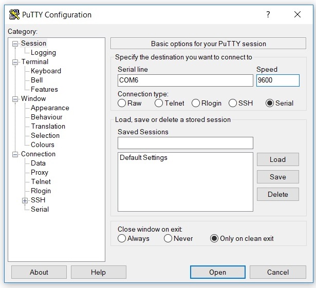
Because the speed was wrong, I got all sort of jibberish back when I tried to test my helloworld
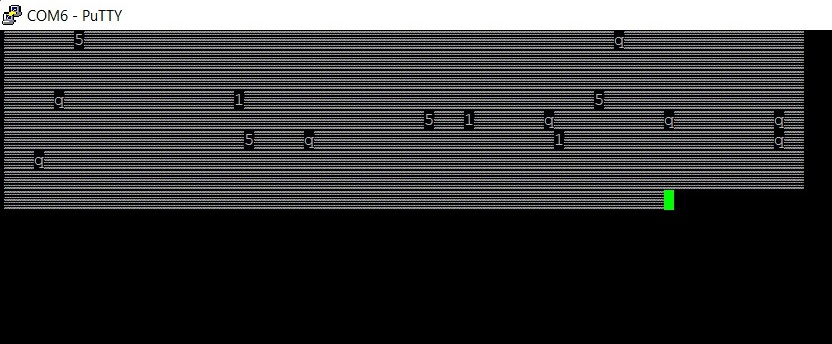
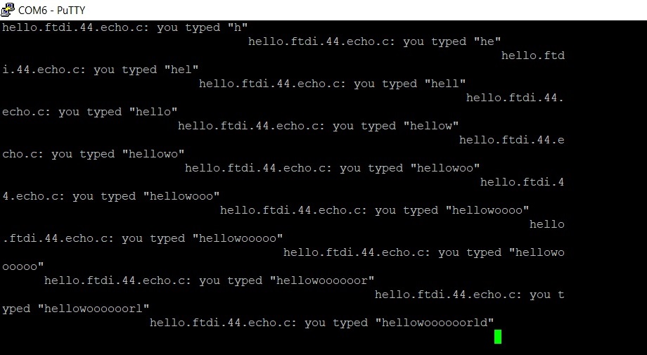
Kati tipped me off that the speed needs to be set to 115200 to be succesful, and finally I got it to work.
Problems had, lessons learned, questions that remain
- I used autoroute to try and draw the lines for hours. I figured that it would have been the easiest way to do this - of couse a computer knows better, right? Turns out no, it was not the easiest way to do this. Once I gave up the auto route I was able to figure this out faster. The result might not have been pretty but it worked.
- Beware of airwires, make sure that you have drawn all your routes all the way.
Copyright © Heidi Hartikainen 2018
Template copyright ©Blackrock Digital LLC 2013-2018

This work is licensed under a Creative Commons Attribution-NonCommercial-ShareAlike 4.0 International License.