Electronics production
Group members
Assignment
Characterize the specifications of your PCB production process (group assignment)
Preparation
Machine: Roland SRM-20
Settings: 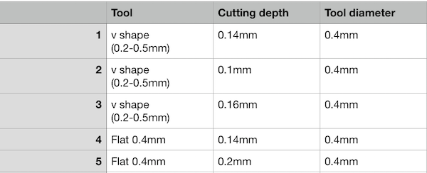
Process
We started discussing which settings should we change and what should we test. We decided to check different cutting depth to see how they differ.
Our assumption is:
- when it cuts deeper, the width is wider than it supposed to be.
- when it cuts shallower, there will be copper left on the surface.
We downloaded PNG files of tracing and outline from Fab Academy website. We convert the files to .rml format in Fab Modules with the settings above.

We saved the files and operated the milling machine. We operated with trace file first with different settings and tools. When we cut the outline with tool diameter 0.79mm, one edge was not cut. It was also mentioned in Nordic review. It was because in Fab Modules there was not enough space in the bottom and Fab Modules recognised that the cutting line is too close and cannot be cut with 0.79mm drilling bit. So we changed the tool diameter to 0.5mm and it cut.


Result
Here is the result. With the tool diameter setting 0.4mm, the thinnest gap the milling bits made was 0.016 inch = 0.4mm (fifth from the right) with both v shape milling bit and flat milling bit. It was because the thinnest tool path made in Fab Module was 0.4mm. It is possible to make the tool path for less than 0.4mm lines if smaller tool diameter is set in Fab Module. When the tool path is made, V shape milling bit might make a gap thinner than 0.4mm, but it is better to use 0.4mm as the thinnest gap in PCB design.
The thinnest trace was hard to measure. There might have been tiny differences in our manual operation and it did not give the clear results, but with flat milling bit, 0.14 mm cutting depth, the thinest trace was 0.004 inch = 0.1mm (fourth from the left). Basically the tool diameter doesn't matter that much to create the thin trace, compare to creating the thin gap, since the milling bit removes the copper around the trace lines. However, as our result shows, the outcomes can be affected by operation of the machine and too thin lines can be removed. It would be safe to use certain thickness, according to our result at least more than 0.1mm, for trace lines in PCB design. 
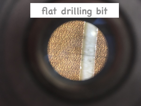
After cutting boards, we looked at the surface with microscope which has measurement scale.
Tool difference
With v shape bit, we could see two lines on the edges of the trace. Since the bit is v shape, the tracing width is different between the deepest point of the bit and in the point of the surface. The point which is closer to the surface, the trace width gets wider. On the other hand, the trace lines of the flat drilling bit is just a single line on the edge.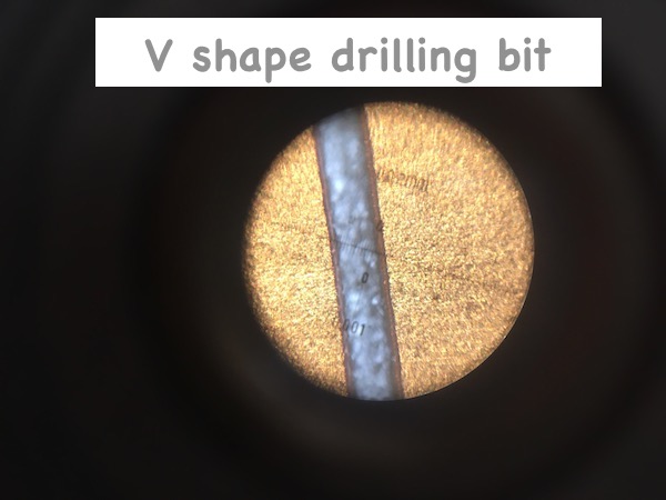
Shallow cutting depth
There was copper left on the surface of some parts of PCB. However, probably it was not because of the tracing depth, but because the surface was tilted, since copper was left only some parts.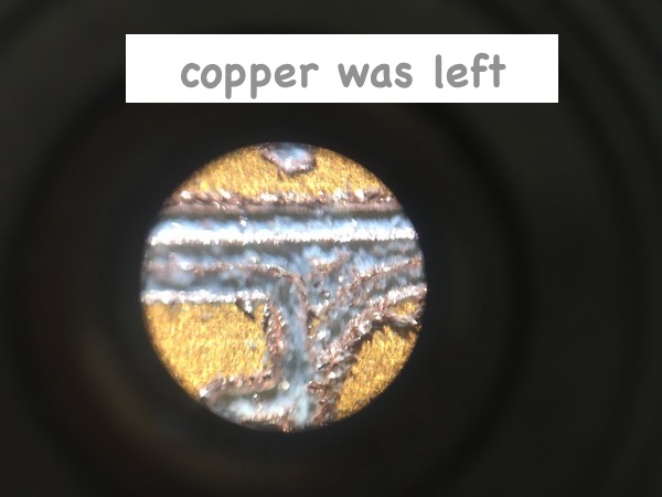
Deeper cutting depth
It looked different, with the deeper cutting depth settings, more the copper layer was removed and the tracing paths looked wider. However, it was hard to measure the exact width of the tracing paths with microscope.