Abstract
This week was about electronical design, about how to assemble components with Eagle, how to switch from the schematics to the board representations.
The question raised were:
- How to translate a board representation into schematics?
- How to optimize board space?
- What are the limitations of an autorouter?
- What inter-sofware workflow to pick? For which purpose?
- How to simulate board?
The main obstacle was laying out the components in order for the traces not to cross. This requires some practice.
The basic rules being: don't build a GND/VCC loop, make sure that a corner stays free so that the problematic wiring find a path.
Try to minimize traces, if a component need to be at the ground place it on the outside.
I mainly used 1 workflow:
- Eagle > Gimp > mods/fabmodules > VPanel > circuits.io
My biggest achievement: Having my board soldered Friday evening
My biggest struggle: Routing all the components
Chronology
| Thursday | Friday | Monday | Tuesday |
|---|---|---|---|
| Introduction to electronics | Component change (FTDI: SMD >THD) | Simulation tests | Documentation |
| Eagle schematics | Png export and vectorization | Website reworking (source files, image proportions...) | |
| Board arrangement (with help) | Milling | ||
| Soldering |
Setup
| Softwares | Fonction |
|---|---|
| Eagle (+ fab.lbr) | Drawing boards (additional library) |
| 123D circuits.io | Board simulation |
| LTSpice | Board simulation |
Skills acquired
Asssesment validation
The first step after having installed Eagle was to add the FabAcademy library to the Eagle librairies. Once done Eagle could be launched, a new project created and, inside it, a new schematic. Components were added one by one by clicking on the Add icon. All components except the through hole FTDI could be found in the FabAcademy library. Funny fact, FTDI seems to be a company name not a component one.
FabAcademy library addition
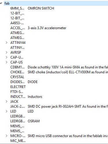
FabAcademy library content

adding a 1206 resistance
Wireless connection
Instead of tangling wires linking each and every legs wireless connections based on names can be set.
First short wire extensions with Net need to added to the components, then named with Name. For better visualization use the Label option.
If two connections are given the same name Eagle will detect it and ask the user if he wants to link the two.
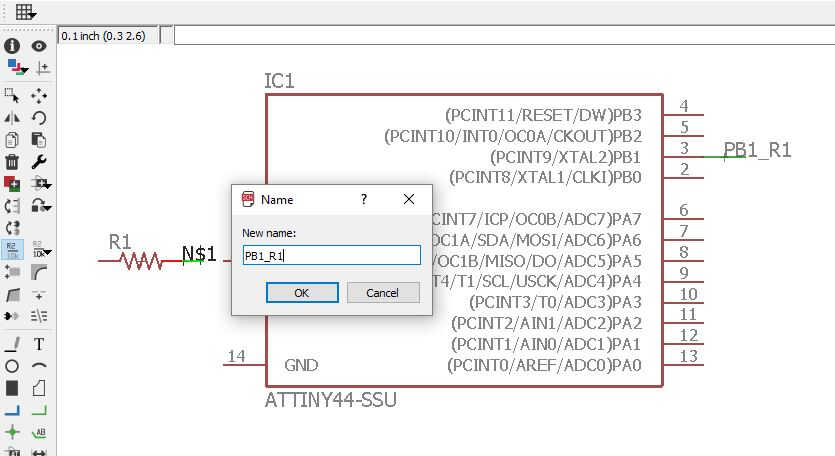
Setting a name
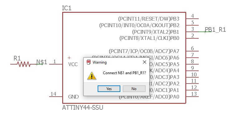
Automatical wiring
The resonator was replaced by a crystal and 2x22pF capacitors. Without capacitor the crystal wouldn't be reliable.
A 10 kOhm pull-up resistance was added to the button.
A pull-up resistor pulls the voltage of the signal it is connected to towards its voltage source level (high logical level).
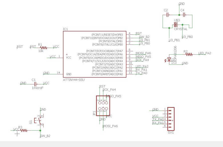
schematics final
Setting a name
Automatical wiring
Once the schematic done the ERC tool needs to be run. It will check the connection, the values...
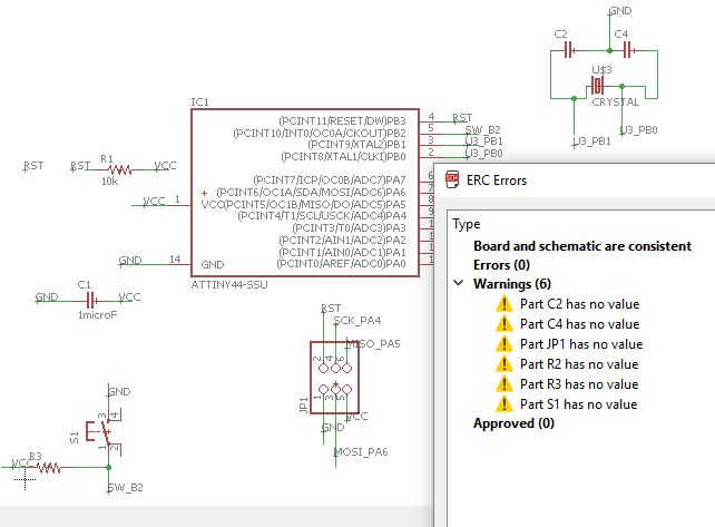
electrical rule check
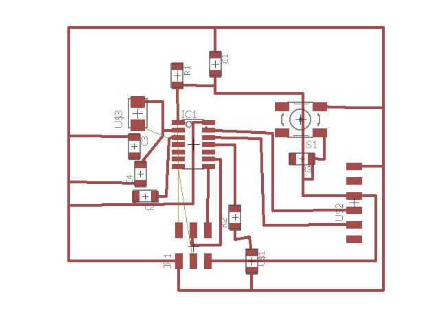
If everything is ok it's time to switch to the board view, which is a more realistic view of the board.
Source file to load here
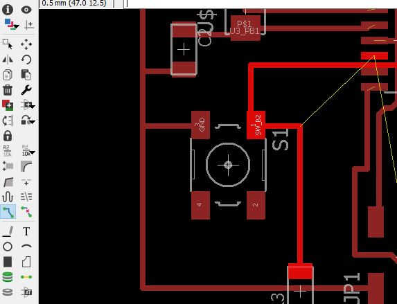
Components are wired with thin lanes, which represent the connections defined in the Schematics section. It's now time to untanggle. The rules being:
- Optimize both sides of the microcontroller (you may have to go back to Schematics to do it, that's what I did as I first branched the button and the LED on the same side)
- First join all the ground connections together, same for the VCC ones
- Don't form a closed loop with GND and VCC. Take care to leave a free corner
- Components which need ground connection should be the closest to it (ex: the crystal capacitors)
- Tracks can go inbetween components legs (except for the through hole FDTI)
- 2 tracks can be drawn at the center of the microcontroller
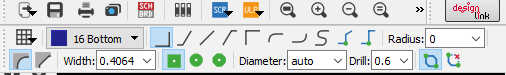
- When possible replace 90° angles with 45°. The can be found in the toolbar when using thee Route tool. This create less resistance to the current.
Components are wired with the Route tool which is constrained by the relations defined in Schematics. Once you click on a leg to connect the legs it has to be connected to will light up in red.
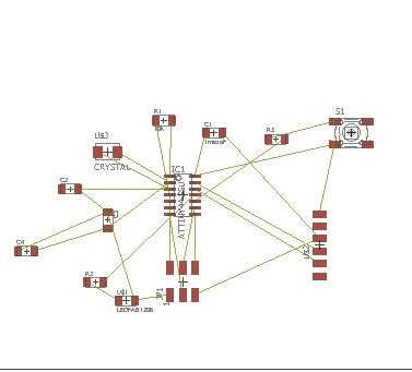
Board view start
Routing guide
First try at routing
Once the Vcc and the ground are separated, the most trickiest part is done. If you are stuck the Autorouter tool can be of great help. It will compute routes without moving the components nore the already existing wires. First select the layers you want to use -in our it was only top- otherwise it will tend to suggect a double-sided design. To make the routing exercice a little easier go to the Grid tool and refine the size up to 0.1 mm.
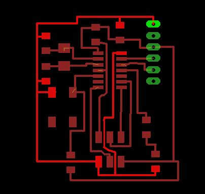
Ground
VCC
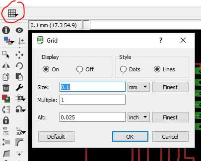
Grid tool
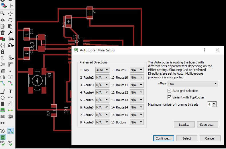
Autorouter
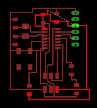
Design check and optimization
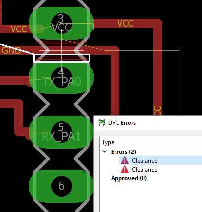
Once the routing is satisfactory, optimize the space by packing the components closer to each (not to much to be able to solder) After this test the design with the DRC check tool. The only parameters rules than we changed were the clearance one. All values in mil were replaced by 0.4 mm. If clearance errors are detected by the DRC check try to reduce the trace width with the route option width (go down to 0.3 mm).
DRC parameters -spacing-
distance check
Route options
The routes can still be optimized, by reworking the wires angles (45° preferentially) and with the help of Polygon option. The polygons make it possible to create ground and VCC planes, those planes considerably reduce the milling work. Here a tutorial to help with VCC/GND planes:
I didn't have time to design planes so my board was made without.
Source file to load here
Png export
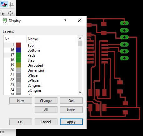
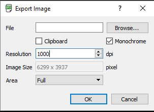
Now the board design has to be exported in a .png format. To do so Export as image (File > Export > Image) with the layers of interest selected. First I exported the traces: I removed all layers from display (None option) then I selected the top layer (1/red) and the pads (17/green). For the outline export I selected the dimension and the pads layers. The dimension is the representation of the board contours. I reduced the board dimension to the board size first. In the export option the Monochrome option needs to be ticked and the resolution at 1000 dpi.
trace layers
export as image
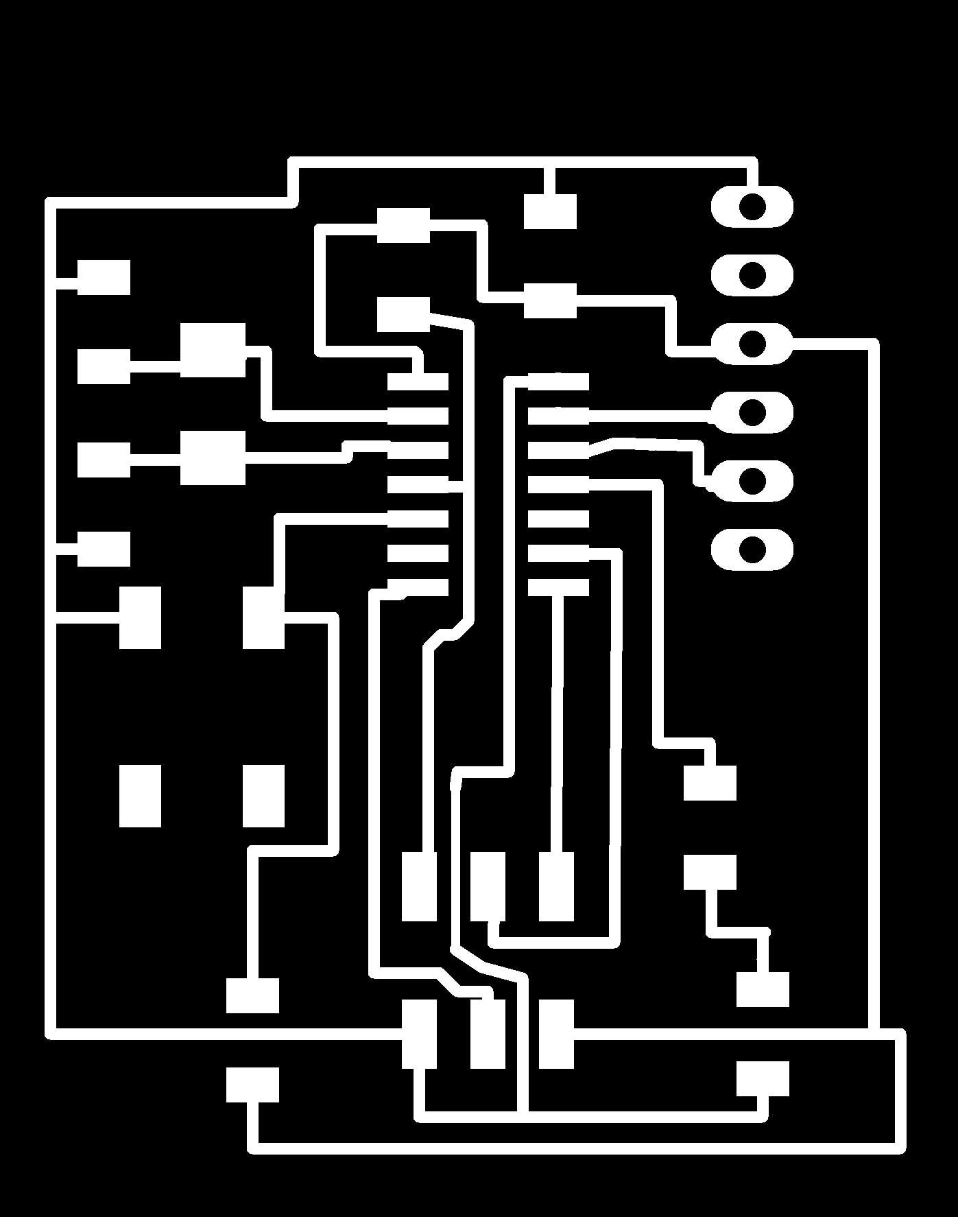
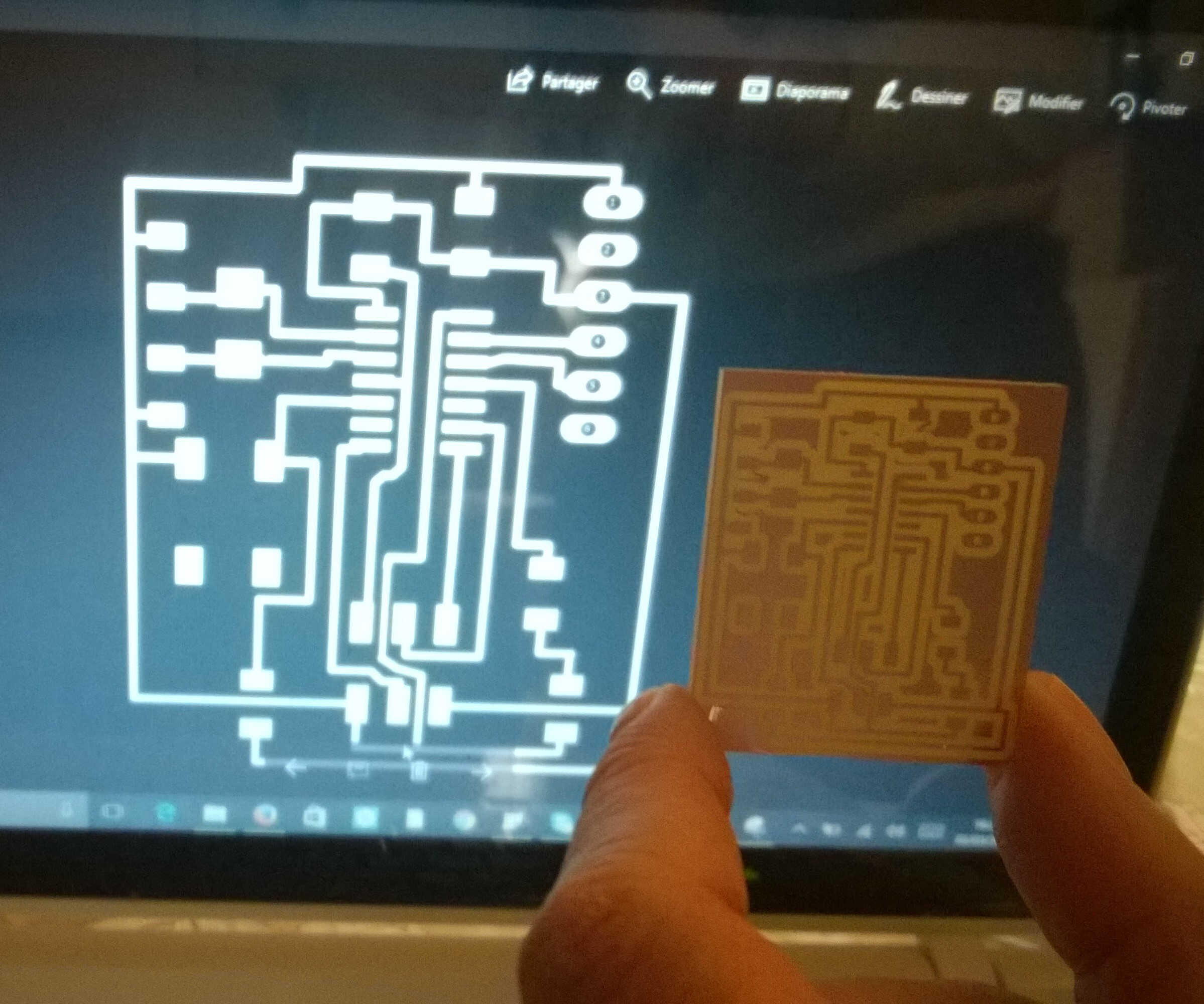
exported traces
exported outline
exported outline reworked
The outline needed to be modified as the central part should stay white. I used Gimp to do so, with the Pipette and Filling tools. There was a small export bug and the pads number remained after export so I also used Gimp to removed them. Also the external outline was too thin to be vectorized so I thickened it with Gimp tracing line with the Brush tool + shift.
Source file to load here
Mods/Fabmodules
Now that the png files are correct I could input them to compute vectors as seen in Week 4. I tested Mods. I succeeded in producing the vectors but didn't know how to save an rml file so I switched back to fabmodule. I could notice small change in the vector between the 2 outputs.
Mods workflow
setting x0/y0 in Mods
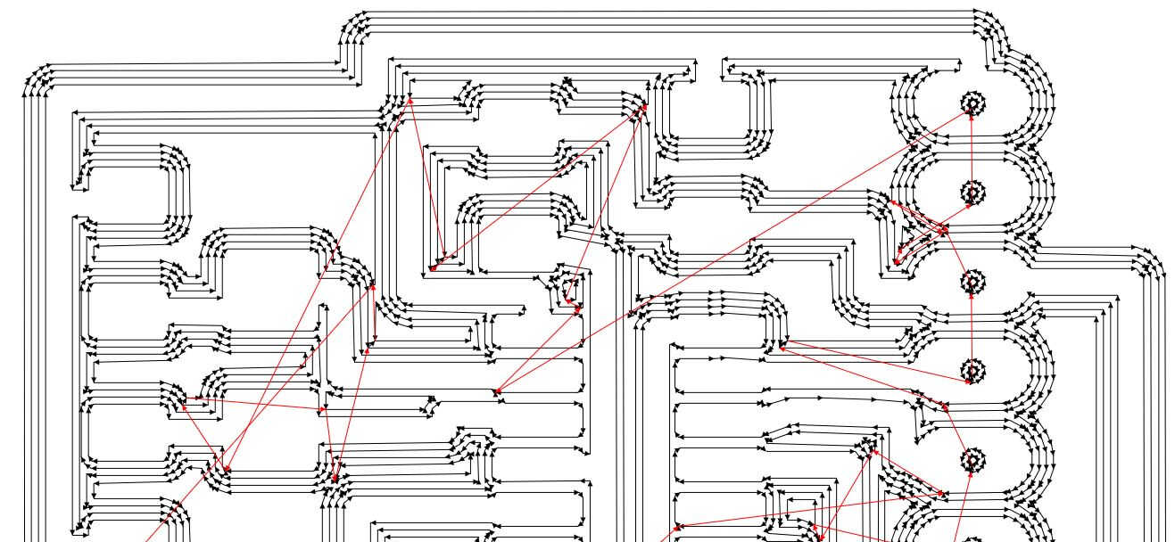
Mods vector

Fabmodule vector
Source file to load here
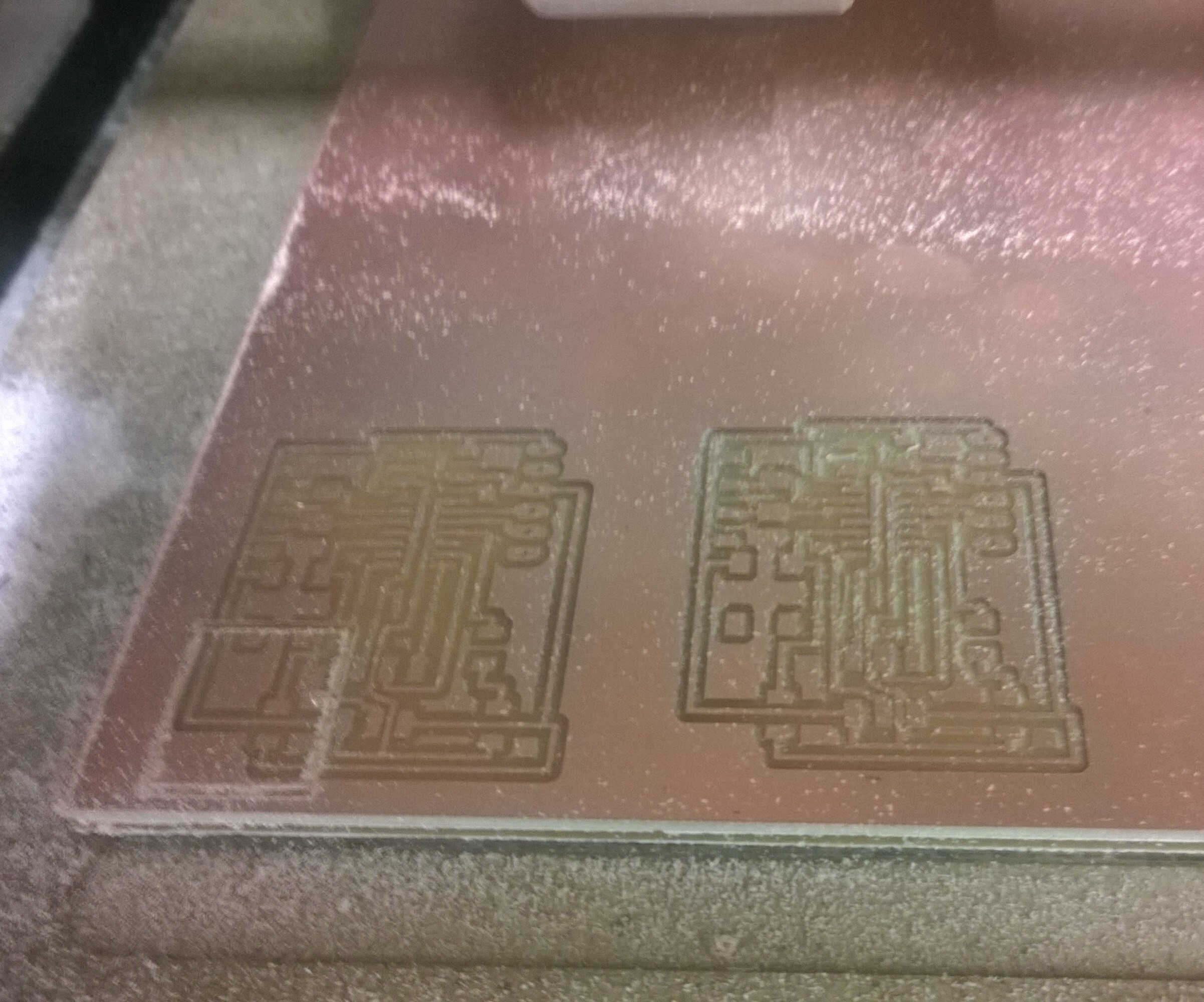
Milling
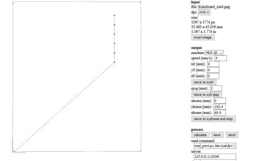
Go back to week 4 for details on the milling workflow. Here I will simply expose a small mistake I made. In fabmodule instead of SRM-20 I selected MDX-20 as machine. MDX files are slightly lighter and result in cuts of smaller dimensions. The same could happen if the 2 files don't have the same resolution.
wrong machine
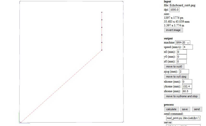
SRM-20
output
mill check
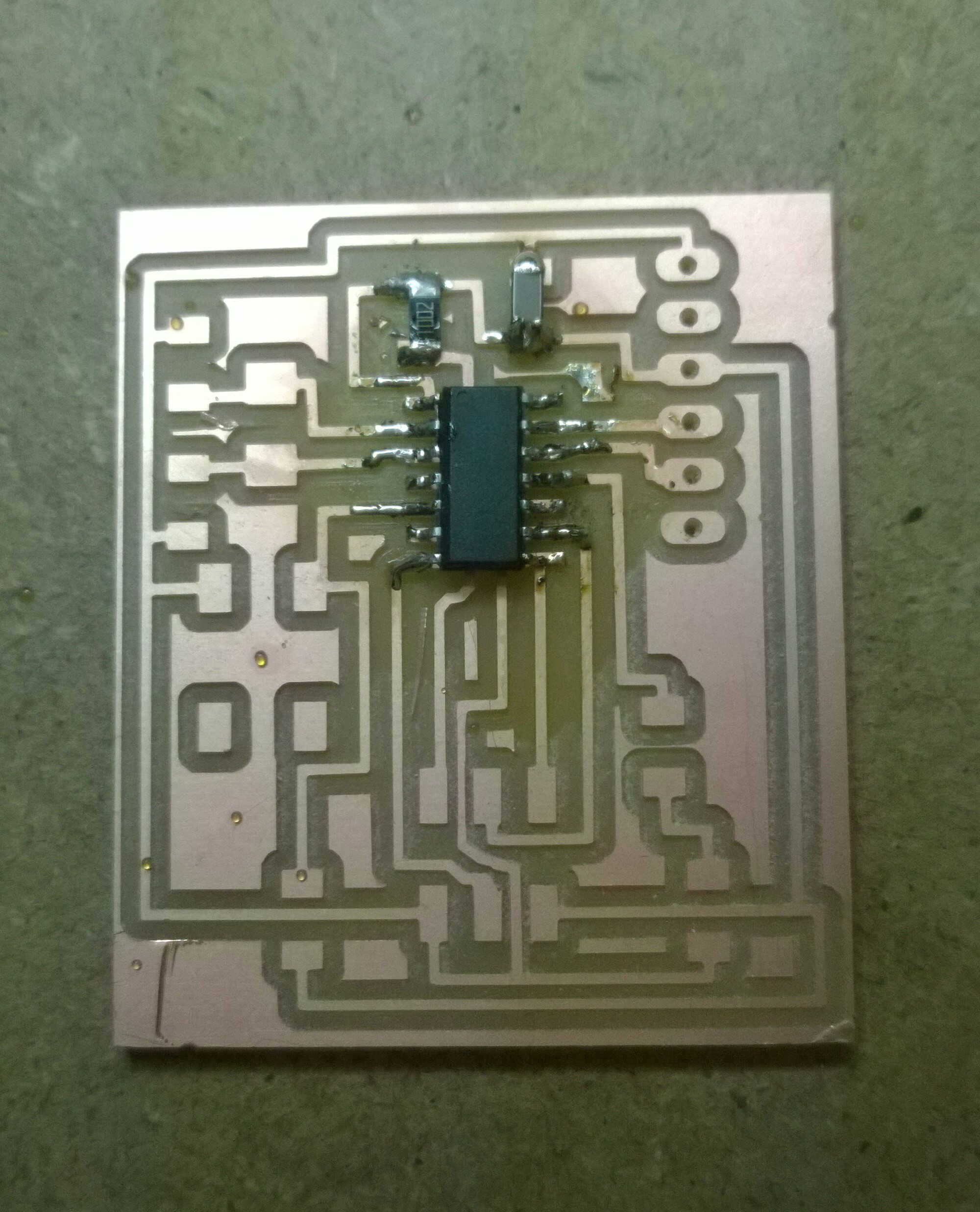
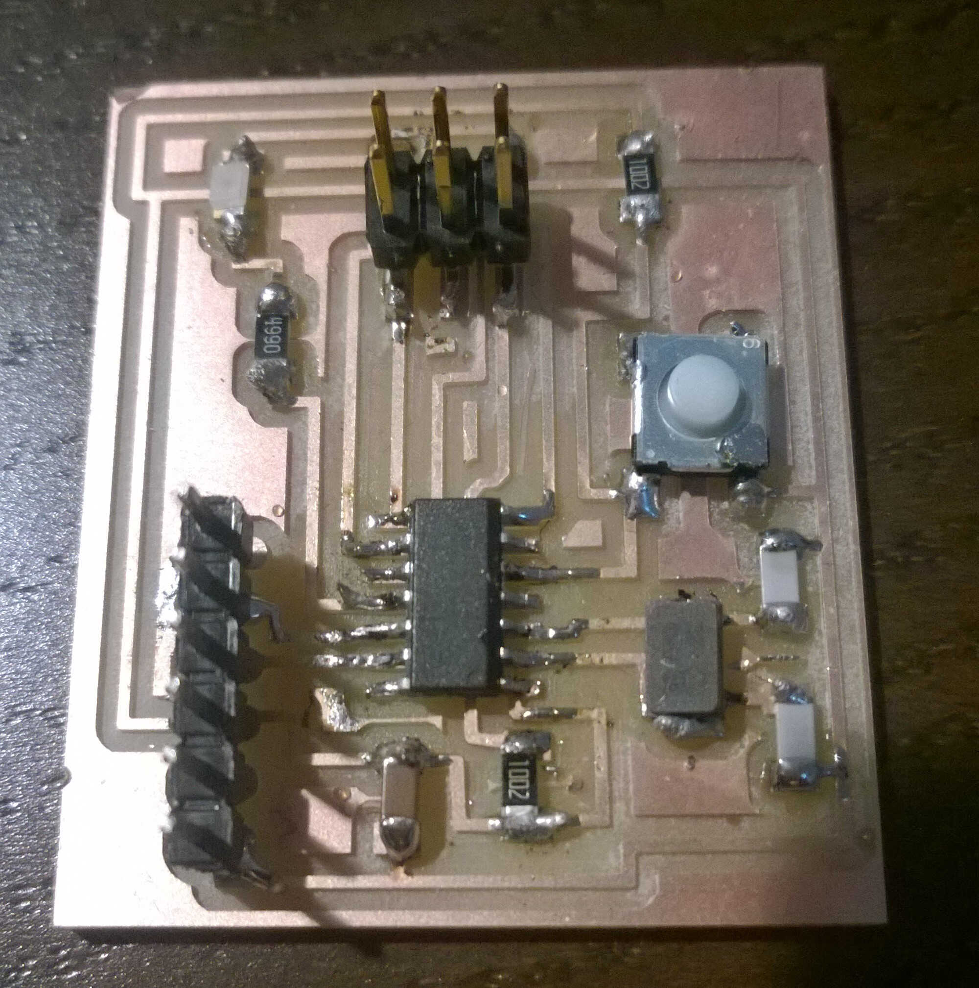
Soldering
The components were gathered:
ATTiny 44-SU
FTDI 6 pins
2x3 header
2x22pF and 1 microF capacitors
1 red LED
1 button switch
2x10kOhm resistors
1x20MHz crystal
LED resistor, value to be computed
The soldering process was similar to the one explained in Week 4. I tried to use Woma's flux (a ROL0 one -rosin with low activity and low halide content) with relative success so I went back to the old school method. "In soldering of metals, flux serves a threefold purpose: it removes any oxidized metal from the surfaces to be soldered, seals out air thus preventing further oxidation, and by facilitating amalgamation improves wetting characteristics of the liquid solder."
Soldering the microcontroller was problematic due to the tip width of the soldering iron.
Also problematic the FTDI soldering, the pads being relatively small. Two options with the FTDI are possible soldering with the pins at the bacl of the board or displacing the plastic part along the pins to make the bottom accessible. I picked the second option.
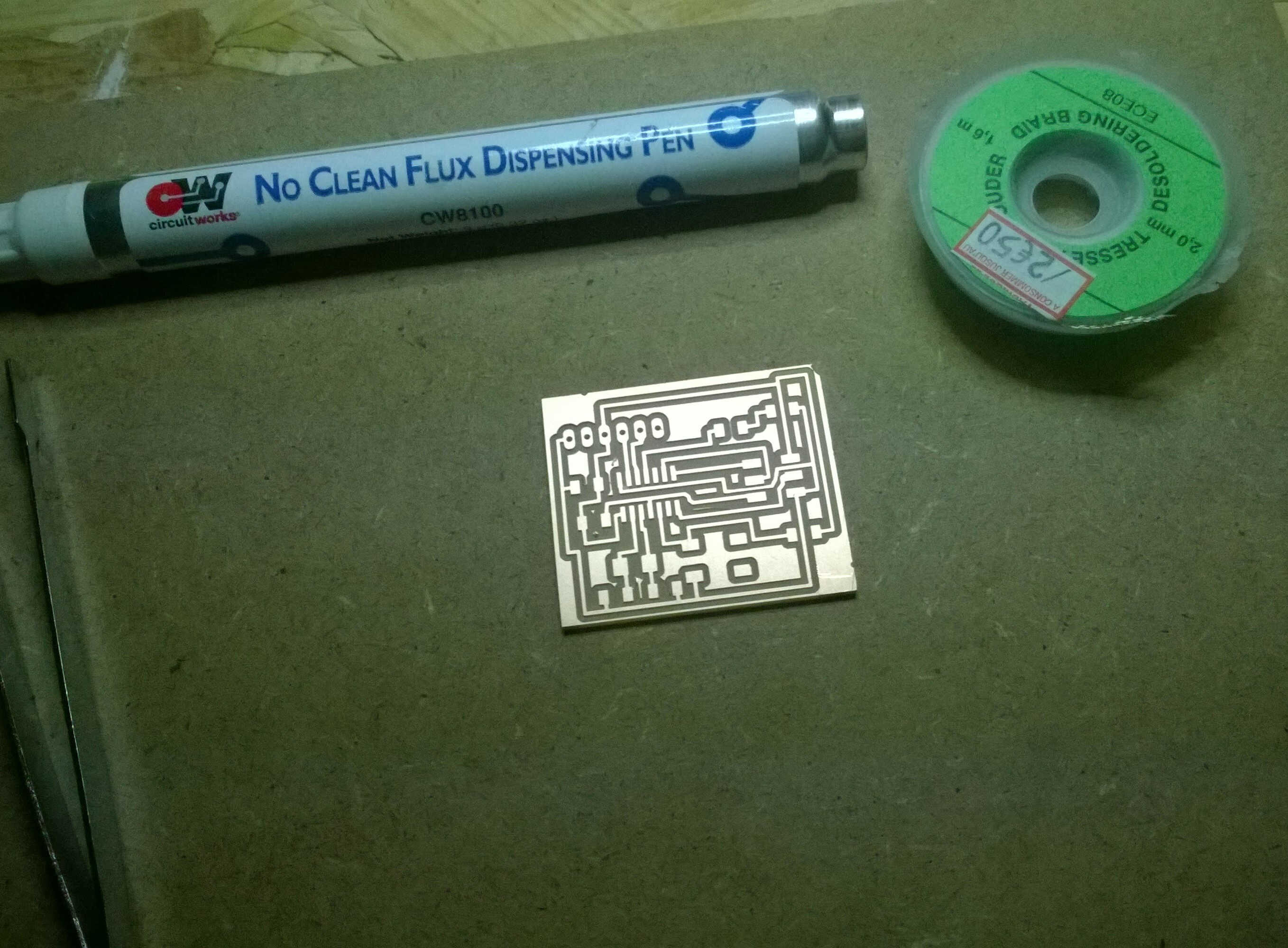
flux try
starting soldering
end of soldering
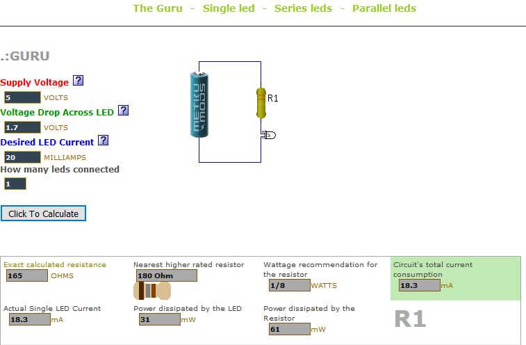
Resistance value determination
A website was used to compute the resistor value. The supply voltage being 5V, the voltage drop accross the LED 1.7 (as I am using a standard red LED and as confirmed with the LED datasheet) and the desired LED currend 20 mA. The result of the computation was 165 ohms. As we didn't have such a resistor I picked the next superior one: 499 ohms. This change will make the LED les bright. Ohm law doesn't apply to LED as they are non-ohmic. A voltage drop is happening in LED. So in order to protect the LED with a resistor we consider the following parameters: forward current and voltage. In this website the theory of LED resitor is exposed.
Vcircuit -Vdrop = 5 - 1.7 = 3.3, then we apply the Ohm law R = U/I = 3.3/0.02 = 165 Ohms. We obtain the same result as the website.
Resistor simulation
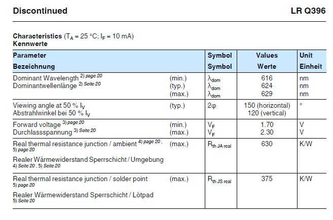
datasheet and forward voltage
Now that the board is soldered I tried to simulate it. I first tried to directly simulate the board as I saw the shortcut Linear Technology on the schematic view of Eagle. I installed Linear Technology Spice XVII but didn't manage to run a simulation. I also made a try with EasyEDA but didn't find the option simulate. It seems to me that Spice codes only work on "pocket" or simplified circuits.
So I switched to Autodesk Circuits. I used 123D Autodesk circuits to model some branches.
1. I created a new project
2. I added an Attiny(smaller than the one we used) paying extra care to its orientation, wired it to ground and power with the dedicated legs.
The 2 lines at the sides of the breadboard are connected along their length as for the middle part the holes are connected perpendicularly.
3. I added a red LED -taking care of placing the long leg to the cathode.
4. I added a serial 499 ohm resistance
5. I added a power source and set the voltage to 5V, wiring it to the bottom ground and VCC lines.
6. I pressed Start simulation to check that the LED lights up
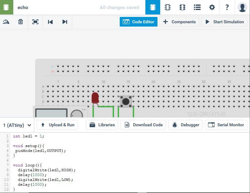
7. I added the switch branch
8. I opened the Code Editor, select the Attiny to program and typed a blink program.
9 I ran the simulation, watched the LED blink and the current oscillate.
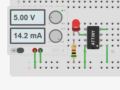
LED powered
Blinking LED
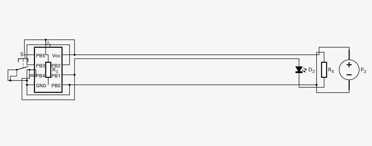
Autodesk Circuits schematic
Autodesk Circuits also provide schematic and board views. The can be used to compare to the original ones.
When having issue with the wiring or the codes it is easy to get inspiration from open-source projects. In the search bar input, for example, the problematic component name and all projects which used this component will come up. Look at the code and run simulation to test them.
Test the design here
Ideas to deepen:
- Two-sided boards
- Flexible circuits build with vinyl cutter and copper foil
Questions raised:
- What electonic board shape will I go for?
- Now that I know how to reproduce a board how can I learn which component to use for mine?
Energy harvesting:
- Supercapacitors have interesting energy storing capacities, to investigate
- Piezo components such as the crystal or the resonator can be inspiration source
Eco-conception:
- Ground and power planes can reduce the milling need
- Check the flux category used
- Check the component datasheet (look for ROHS, energy consumption)
- Build 45° connection to optimize the electron flux
Biomimicry:
Innovation management:
Personnal feedback:
- Good job, well documented
- Need to compress images
Regional review:
Electronical design
- Try the autorouter from scratch
- Forsee the compatibility between the electronics and parts of the final project
- Test the board with ribbon + Arduino IVE
- Try to input a new component in a library
- Use horizontal FTDI
Website
- Add the assignement checklist to the first tab of the week
- Table with link/files
General review:
Website
- Check file size and document this process. Images >700kO to be reduced of 50%/Saved for the web with Gimp. Git commands du or convert (require image magic)
- Colourful titles stand output
- In the personal section represent the interest with icons
Final project
- Create discussion to come up with the proper design for the users
- If every week is devoted to the project: time gain
Week related observations
- Solidworks has some capabilities for moving simulation
- With mods the output is fonction of the cable used (directly connected to the machine)