Setup
| Softwares | Fonction |
|---|---|
| Fabmodules.org | Milling paths calculations |
| VPanel for SRM20 | Communication with mill |
| WinAvr | Programming programmer |
| fts_firmware_bdm_v1 | Programming drivers |
| avr8-gnu-toolchain | XXX |
| GnuWin32 | XXX |
Skills acquired
Asssesment validation
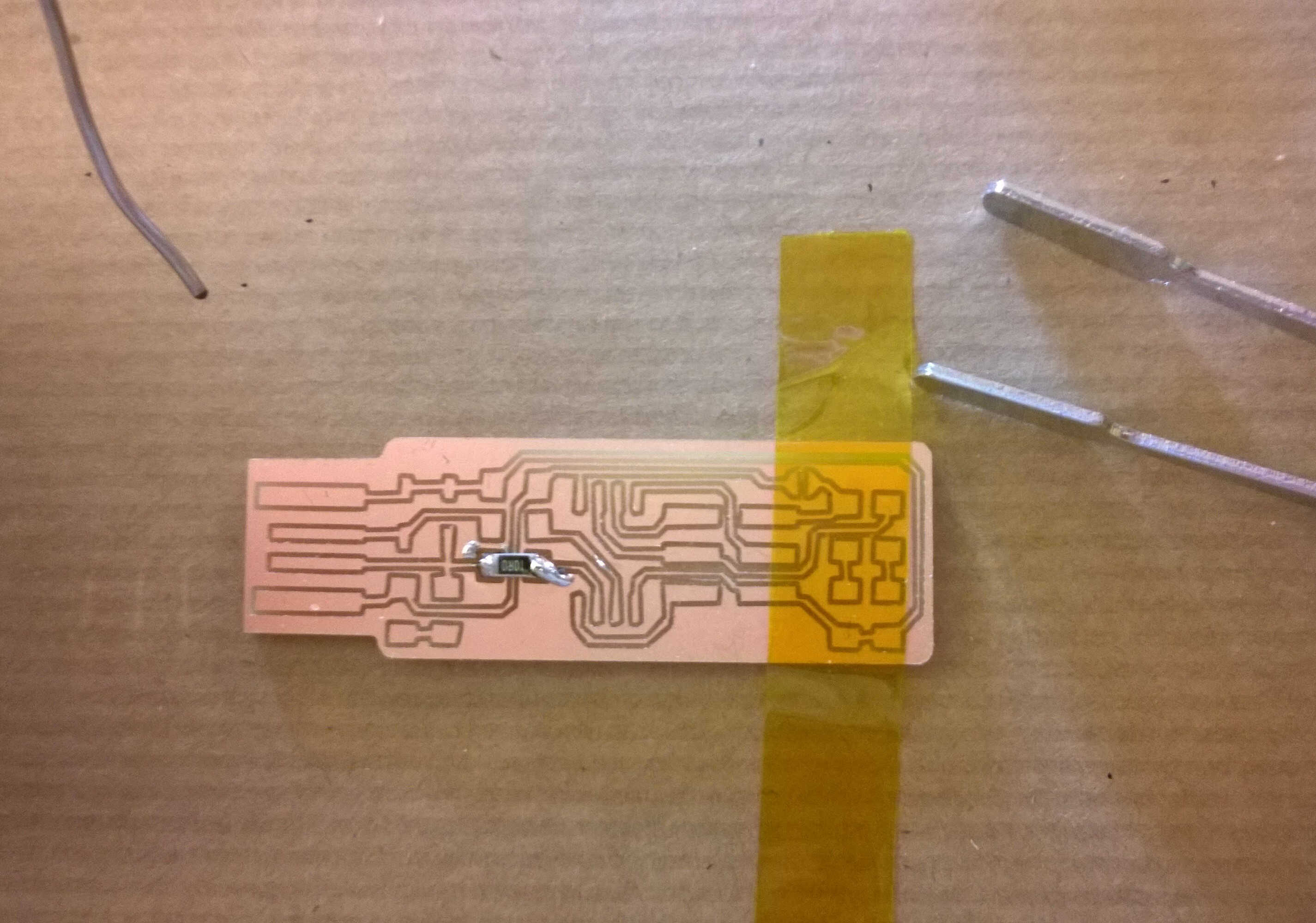
We started with Brian's outlines pictures . We opened them in Gimp in order to replicate them and ultimately to export files enabling the milling of several PCB at once. Each picture was a layer, the outlines and the cutout were superposed. A layer was added to provide a black background the size of the PCB sheet. Otherwise the contours would have been milled as well. Special care should be taken with the picture definition, this should not be degraded along the process.
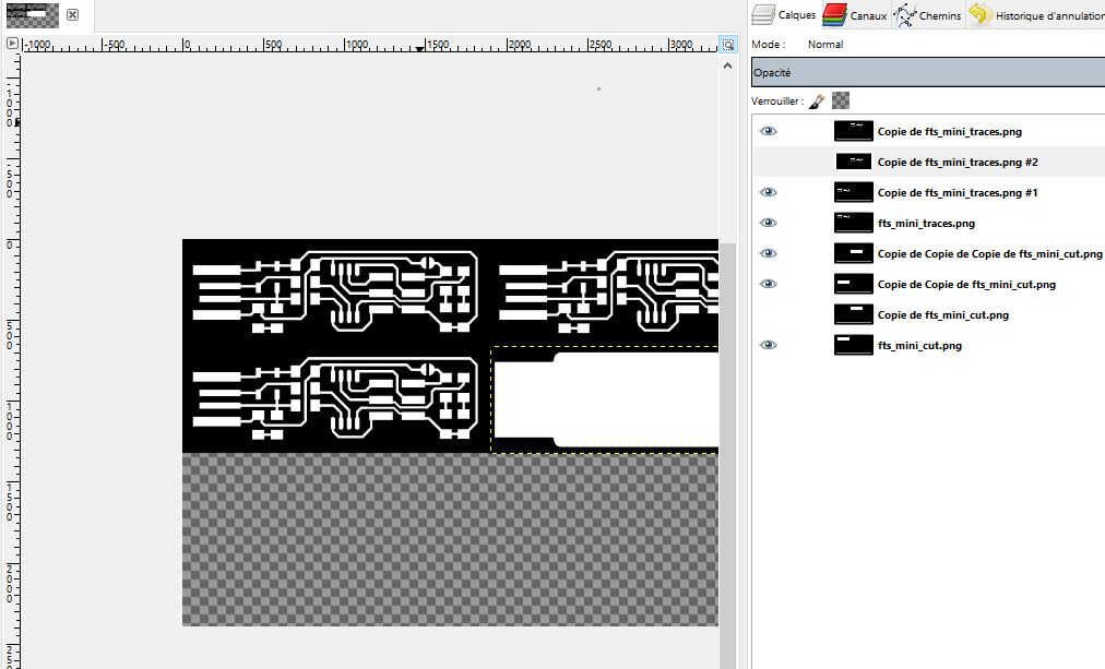
Gimp layers
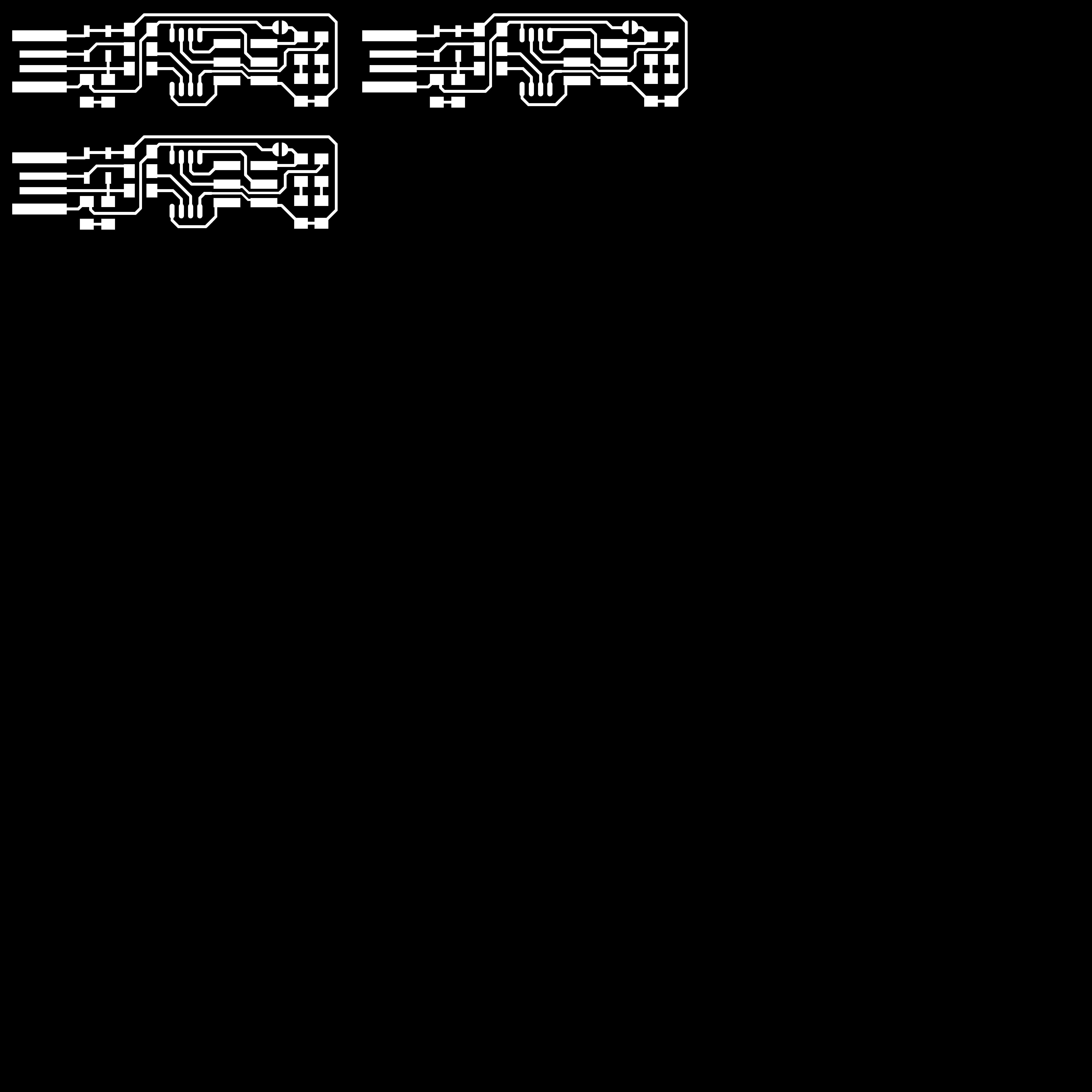
post-Gimp outlines
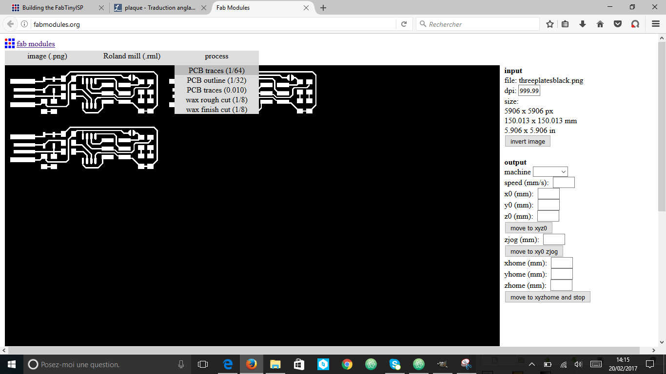
Afterwhat the 2 picture files are imported (in .png format) one after the other in fabmodule.
This module computes a milling path based on the contours.
The fabmodule workflow:
1.Import .png file -Check the file size on the right side.
2.Select the output format (here a file readable for a Roland mill machine .rml)
3. Select the process/drill diameter (1/64 for the outline and 1/32 for the contours)
Some fields will be given values automatically.
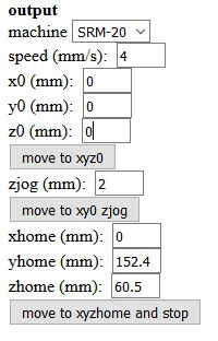
4. Select the machine you will use in the output section on the right side. We used a SRM-20.
5. Put x0, y0 and z0 to 0.
6. Calculate
7. Save, put on USB to plug in milling machine
Fabmodule import
Fabmodule output parameters
Fabmodule process parameters
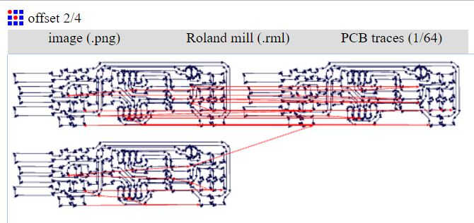
2 offsets paths
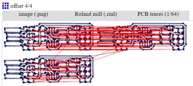
4 offsets paths
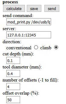
We faced some issues with the parameters. In fabmodule if the machine is selected before the type of process is, then some fields can be empty (x0,y0 and z0 for example). In order to maximize the PCB board space it is advised to prepare files containing 4, 2 and 1 PCB board.
Material
The 15x15 cm PCB boards we used are composed of a base of FR1 material and a coating of copper. It is cheap and made out of hard paper and phenolic resin. As it's not reinforced with glass it's safer to mill as no glass dust will be produced. The downsides are its hygroscopic property and the phenolic resins emissions (small amounts of phenol and formaldehyde -representing a health risk). Phenol resin is frequently replaced with epoxy resin. It is industrially considered as obsolete.
Milling machine
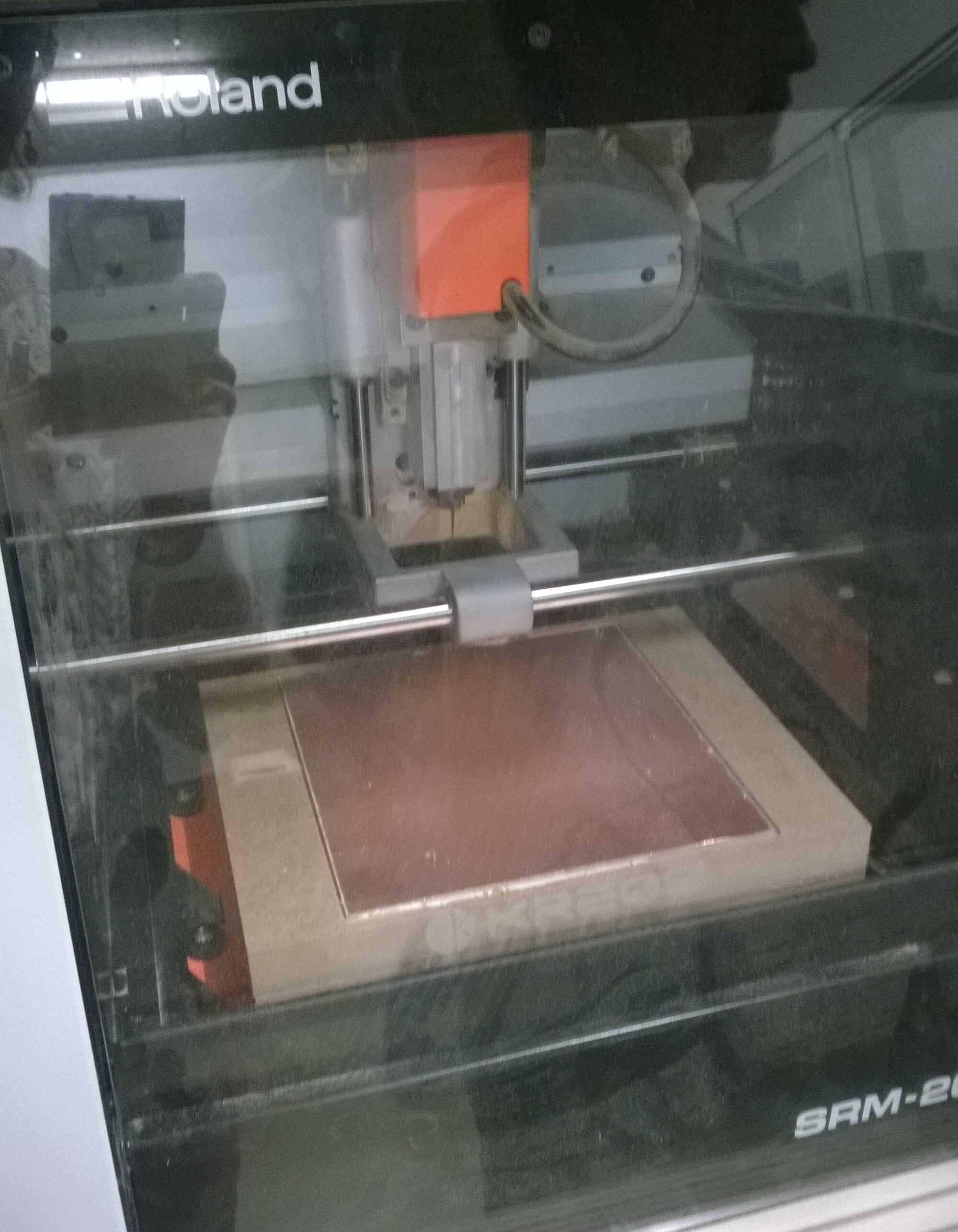
We used a desk milling machine: the MonoFab SRM20 controlled by VPanel for SRM20.
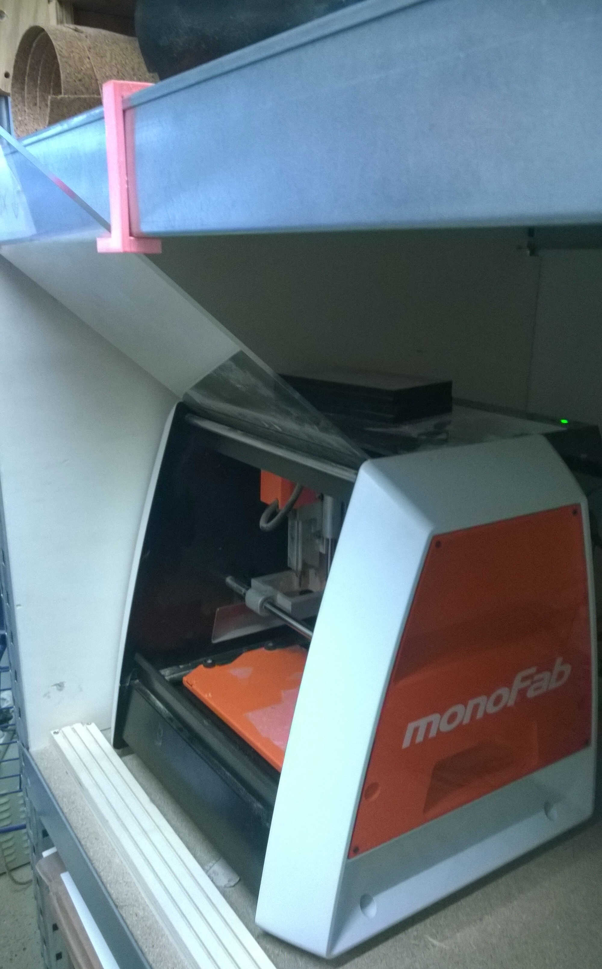
Monofab SRM20
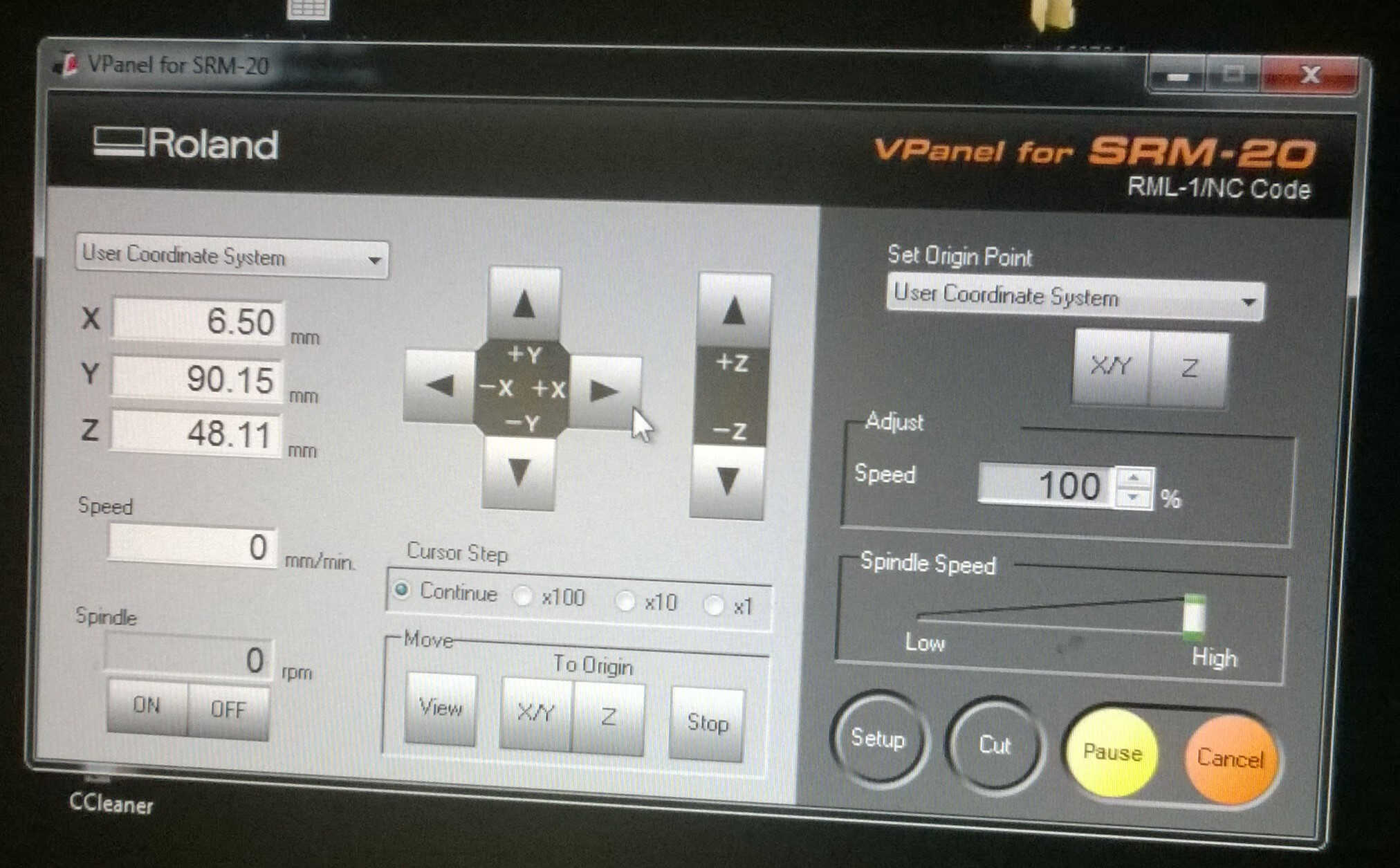
VPanel interface
The protocol to mill is the following:
1. Put a sacrificial layer on the machine bed to hold the PCB boards. Make sure it stays horizontal.
2. Fix the PCB layer on the sacrificial layer with double-sided tape.Make sure it stays horizontal without flexure.
3. Put the right drilling bit.
To do so click on Move > View then unscrew the fixation by turning the lower screw to the left while holding the upper part and the bit with the other hand.
Beware not to drop the bit as it is fragile and beware of their sharpness -they can easily pierce their plastic cap.
4. Use the Vpanel interface to define the origin.
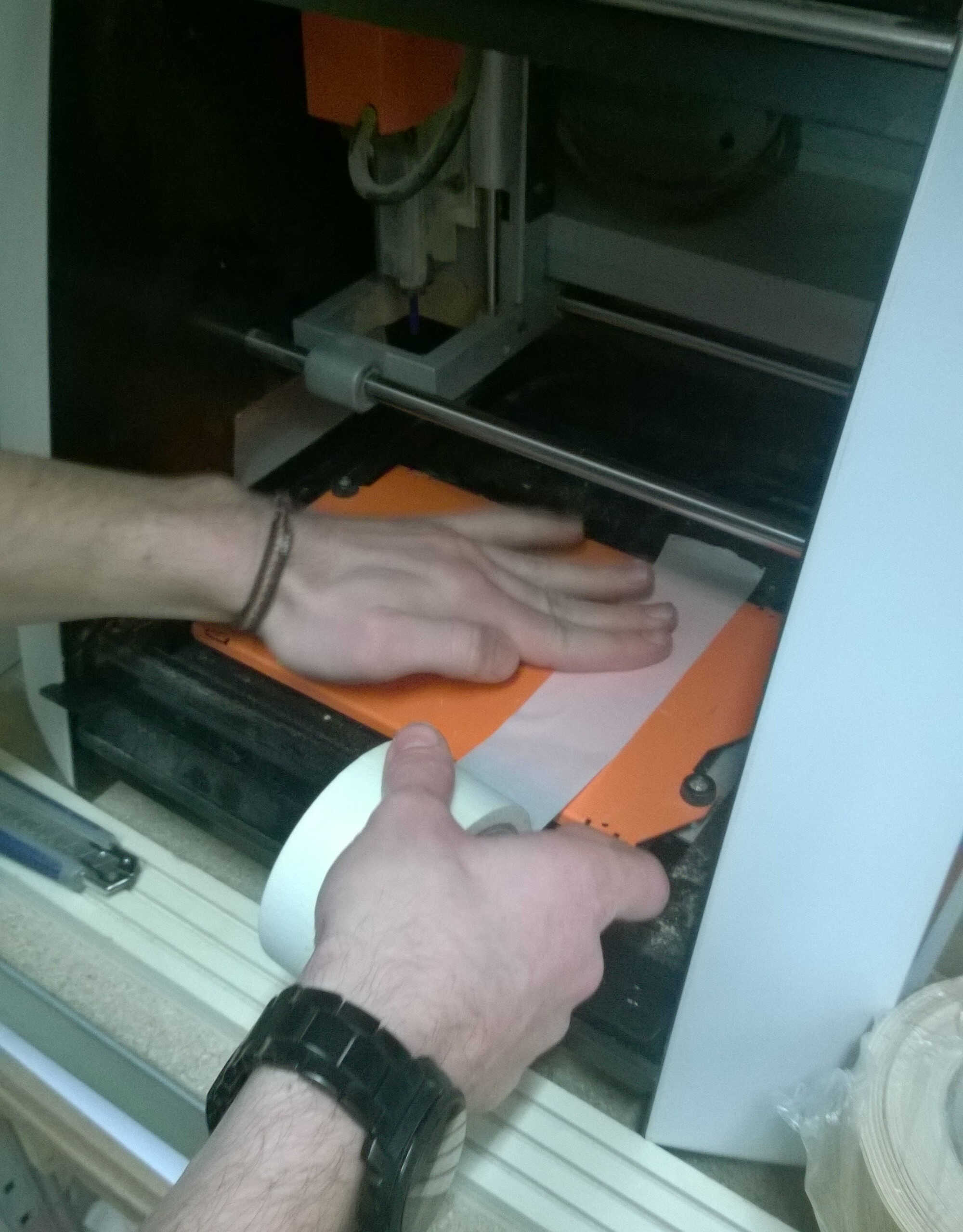
To do the z, use the arrows and the x100 cursor step to get close to the board then switch to x10 cursor steps.
Add a paper sheet between the tip and the board.
When it gets impossible to move the paper the z origin is reached. Click on Set origin point > Z.
Then define X/Y origin. Click on Set origin point > X/Y.
5. Check the parameters -usually 100% speed and high spindle speed- and launch the milling
6. Change bits if needed, make sure you redefine the z origin when you
7. Use a brush to clean the dust
preparing the bed for the sacrificial layer
ready to go (sacrificial layer + bit + board)
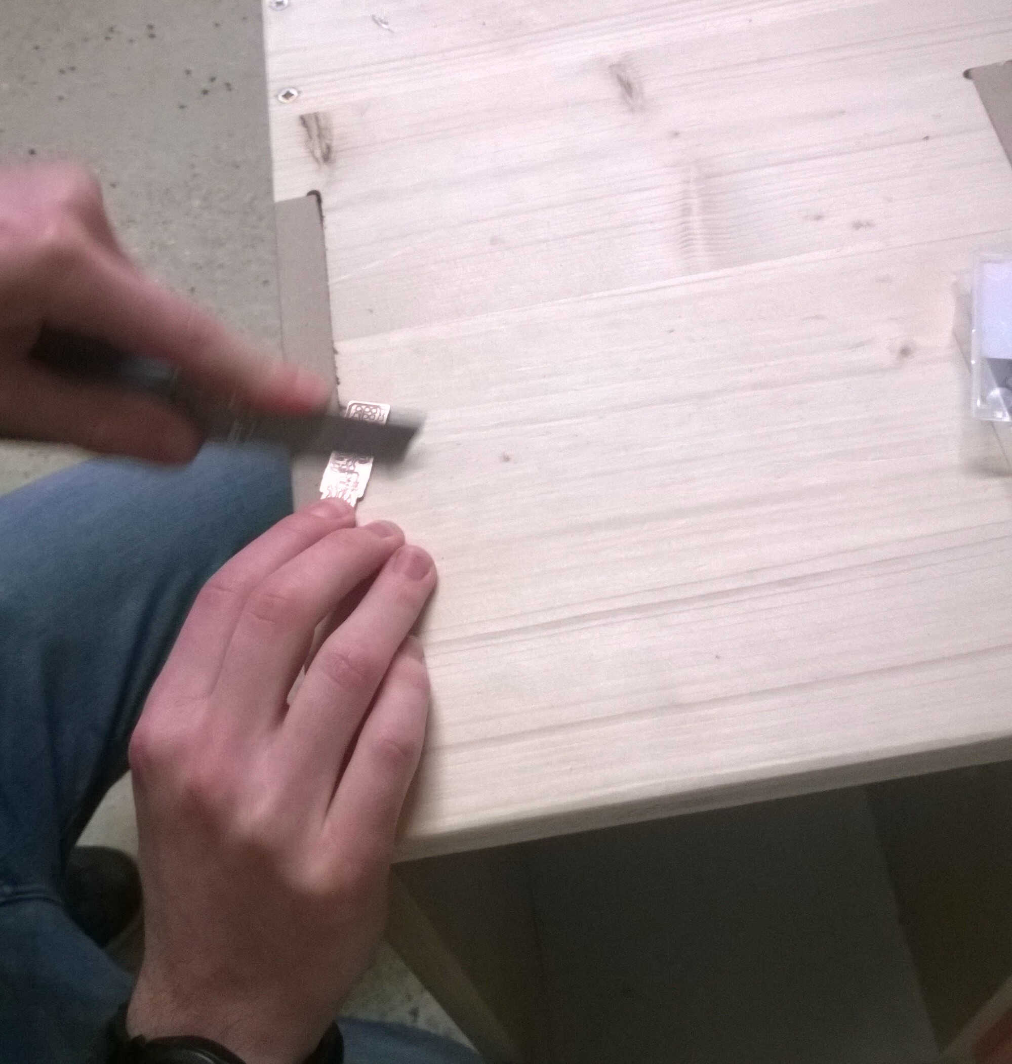
Once milled the board need to be detached with a cutter, cleaned and scraped with the non-cutting edge of a cutter. We could compare the difference resulting of different offset numbers. The bigger the offset number the more isolated the outlines. It is possible to check if the outlines don't interfere with another by using a multimeter. On test mode the multimeter beeps when a current is detected.
scraping
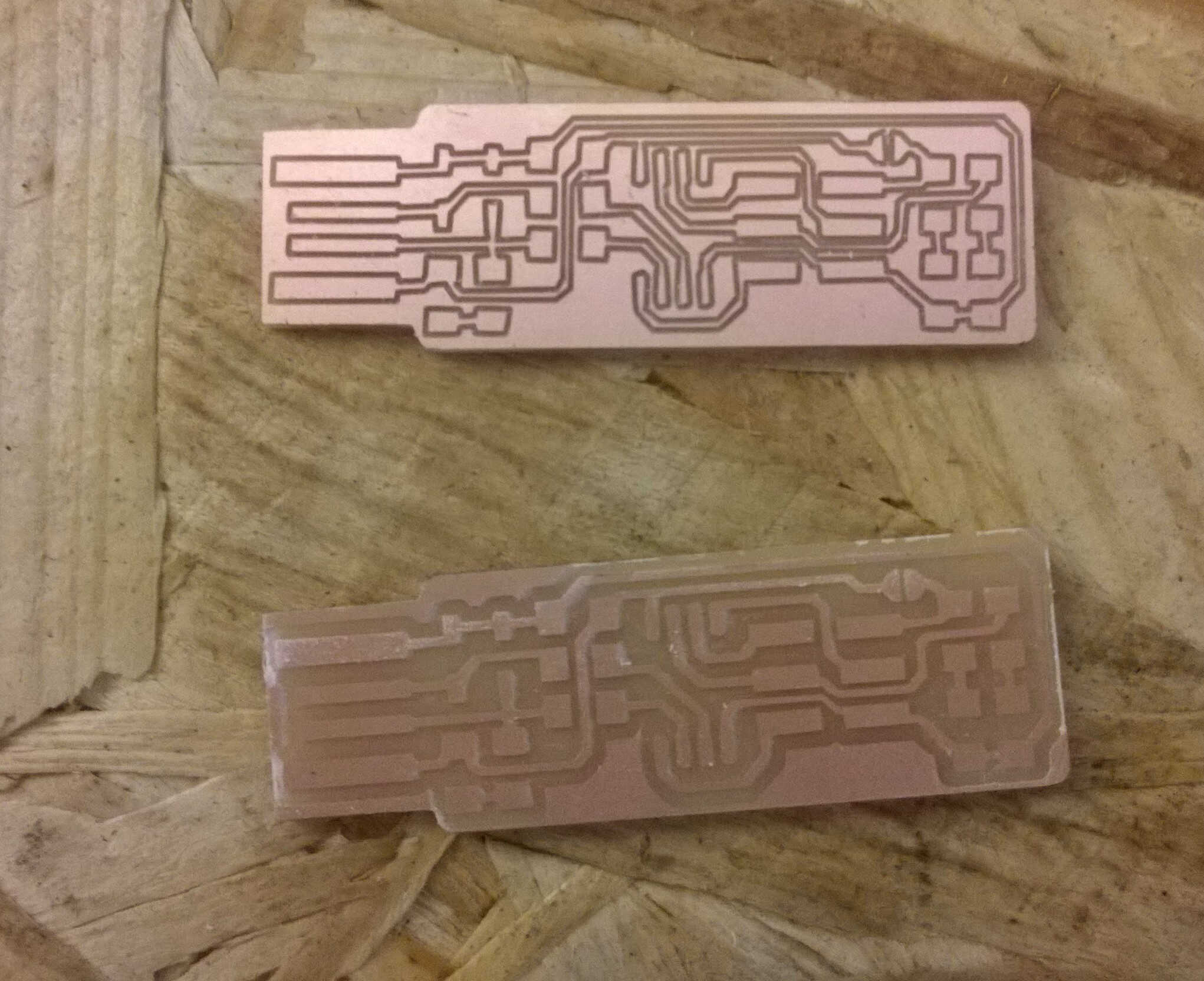
2 offsets (above) vs. 4 offsets (below)
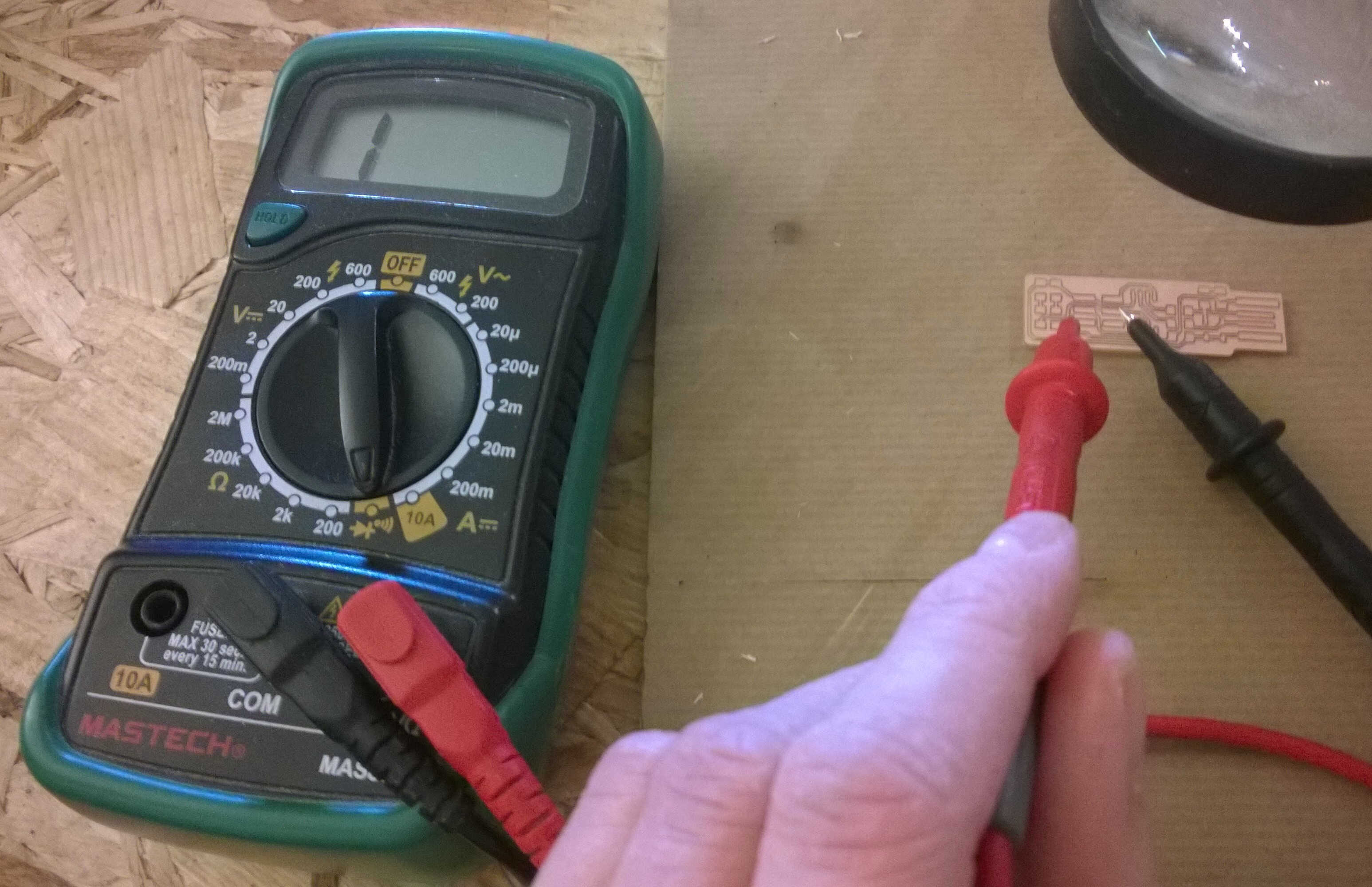
Non-connected outlines tested
Once the PCB board ready it's time to solder components. They are 2 kind of components: the ThroughHoles and the SurfaceMounts ones. We will work with SMD components-smaller in size.
| Tools | Fonction |
|---|---|
| Magnifying lamp | See the orientation of components |
| Storing box | Store and separe components |
| Sacrificial board | Clean work space |
| Multimeter | Check connectivity and component characteristics |
| Solder iron | Heat the solder |
| Solder(Tin, paste...) | Fix components to the board -Beware of lead |
| Metal clamp | Precisely displace components |
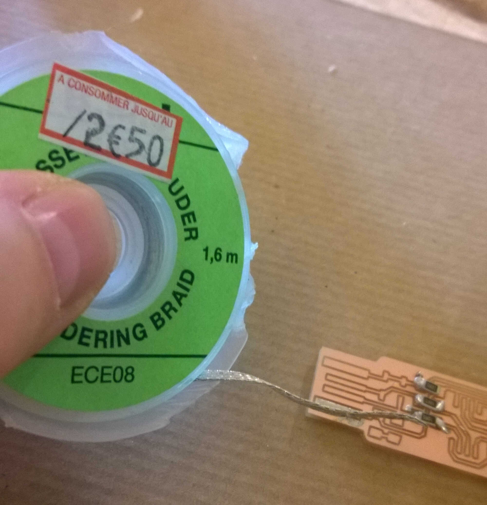
| Desoldering braid | Correct soldering mistakes |
| Thermic tape | Fix the PCB board on the sacrificial board |
| Optional- Heat gun | Correct soldering mistakes |
component storing box
workspace and first soldering
desoldering
The soldering process is thorough. Manipulation inspiration was found on Youtube.
Some precaution should be taken: check that your solder doesn't contain lead and do not touch the desoldering braid while using it as it is highly conductive.
For the polarized components, the magnifying lamp is particularly important:
-a small line indicated the cathode on Zener diodes
-at the back of LED an indent also indicates the cathode
-a small dot indicate the bottom left corner of the microcontroller
Soldering sequence -start at the board center:
1. Deposite solder on the tip of the soldering iron.
2. Apply a solder drop with the soldering tip at a site where the component will be anchored.
3. Use the clamp to place the component at its future position.
4. Melt the solder drop so that the component leg gets immersed in solder. The first leg is fixed
5. Solder the other side.
6. In case of mistake, heat the desoldering braid on top of the solder surplus until it get transfered to the braid.
Once everything is done I reinforced the board so it fits in the USB port with a supermarket fidelity card.s
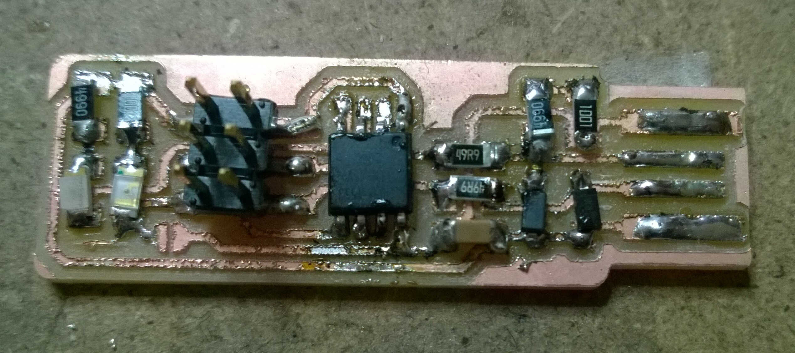
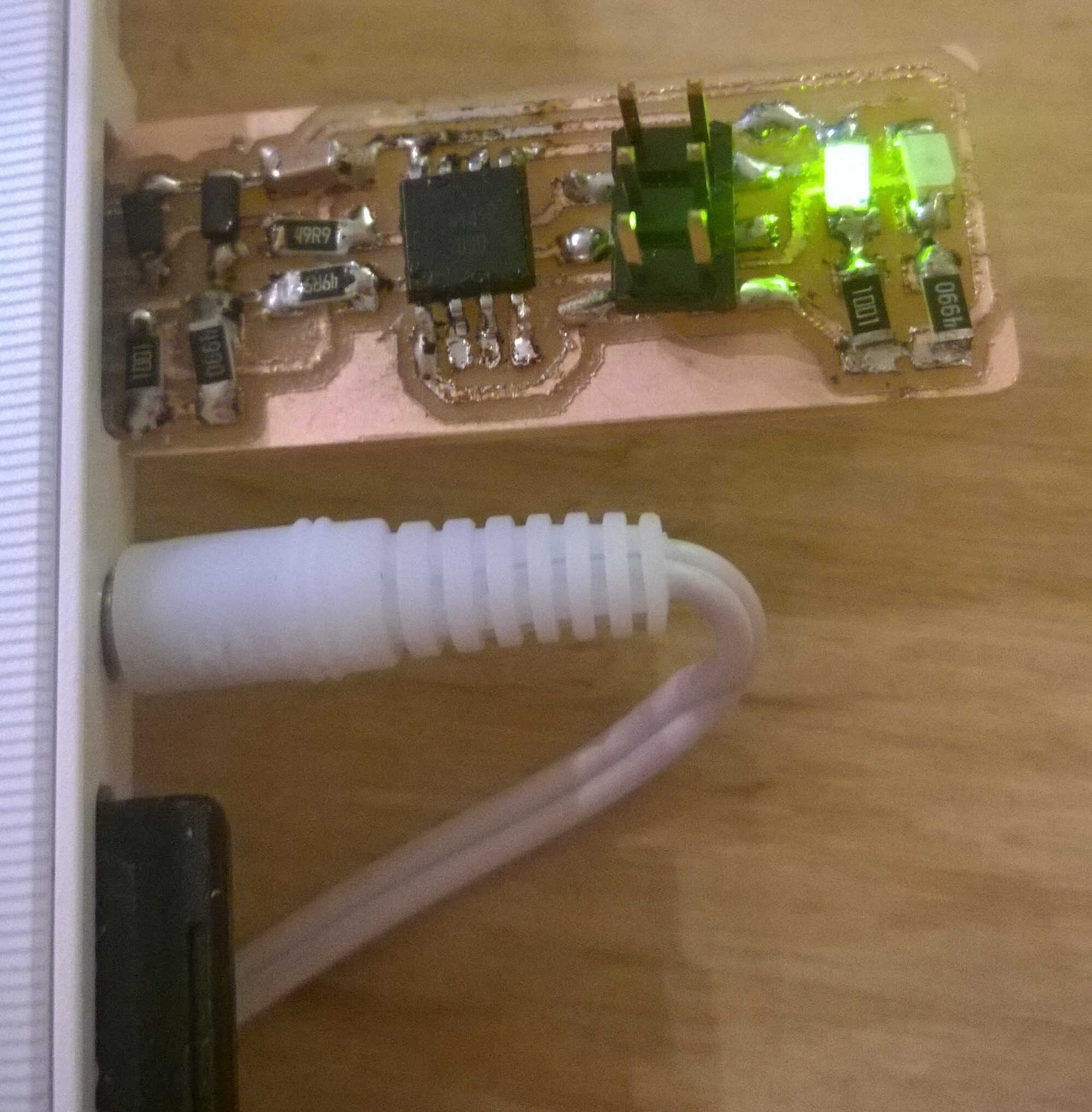
all components
quick fix
A jumper was put to allow programming. Also 4 lines of solder were traced at one edge in order to be compatible with the usb port. Some extra copper was left at the tip of the connection zone, it was removed with a cutter. To make sure I didn't connect legs with solder, I tested their connectivity with the multimeter.
Interprogrammer connection
A programmer can't be programmed with a computer, it has to be programmed by another programmer. Therefore a connection should be established between the board and the other powered programmer. The connection can be made out with a 6-conductor ribbon cable and pitch headers. The header pins need to be pressed against the cable to establish connection. Special should be given to the orientation of the JTAG header (ground should be connected to ground).
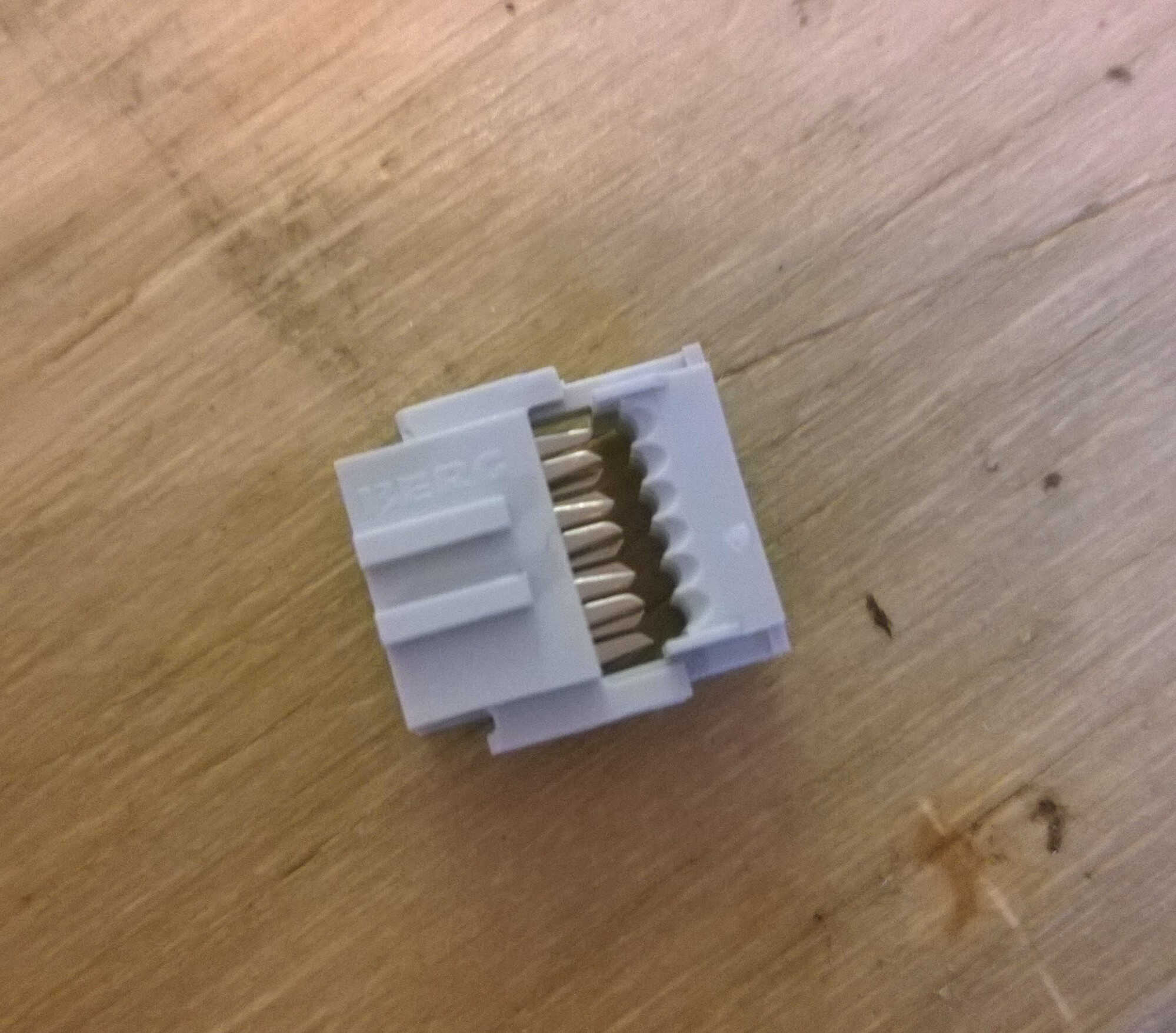
pitch header
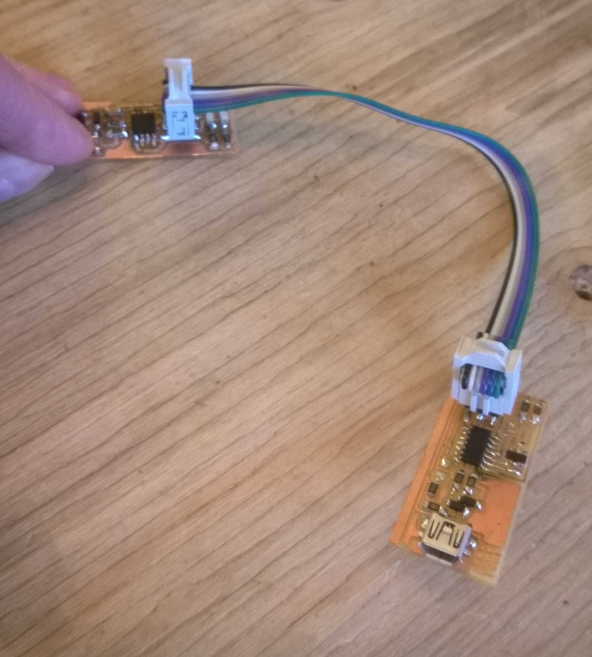
board cables to programmer
Software installation
1. I installed WinAvr based on the Programmation page.
I gave extra care to the system environment variable PATH, copying it in a text file beforehand.
2. I switched to Brian's tutorial more adapted to our board.
3. I installed Atmel Gnu toolchain, Gnu Make and updated the system environment variable PATH by adding paths to those 2 softwares.
4. I downloaded the firmware.
5. I tested those installation in Git Bash (commands make -v; avr-gcc --version and avrdude -c usbtiny -p t45). They all replied to the commands.
WinAvr (avrdude) makes it possible to connect to a microcontroller. I suppose that Gnu toolchain makes a bridge between Gnu and WinAvr.
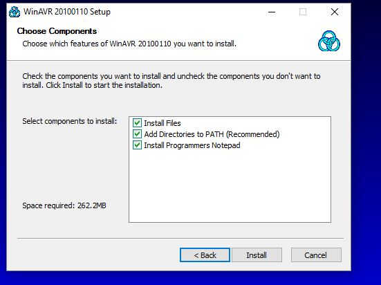
WinAvr installation options
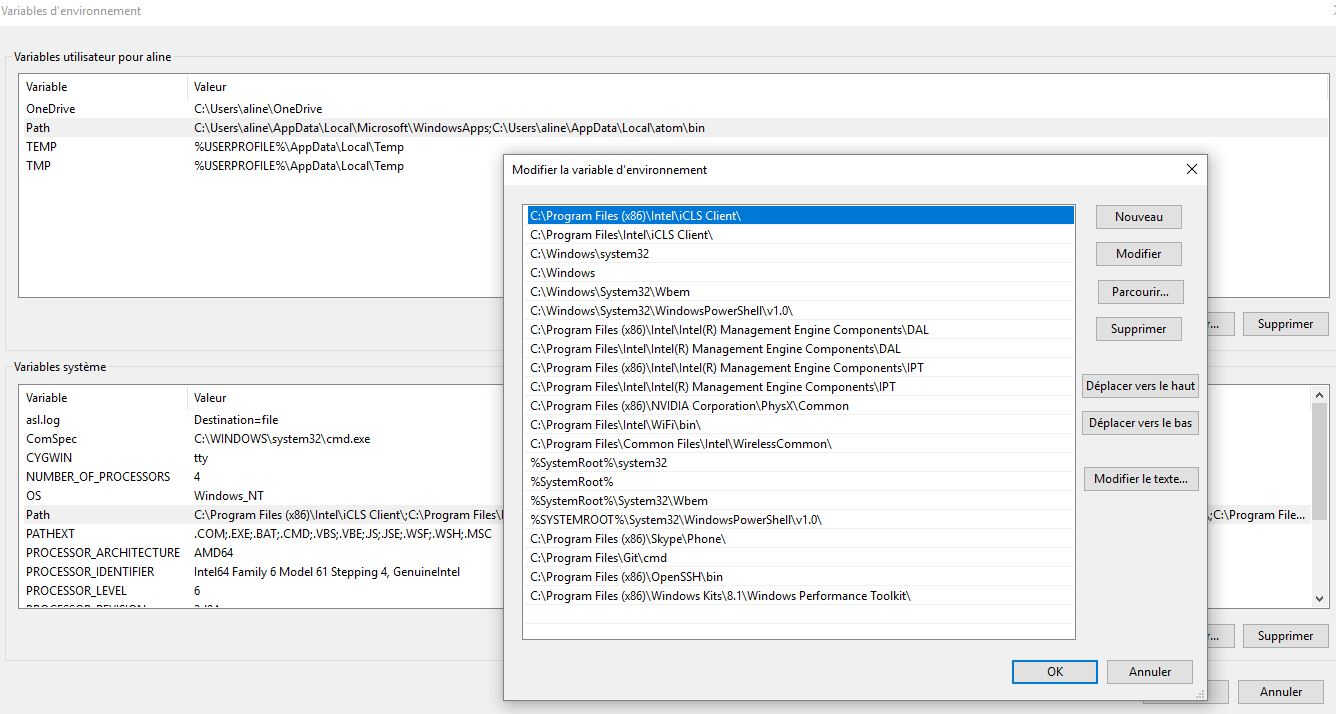
System Path variable
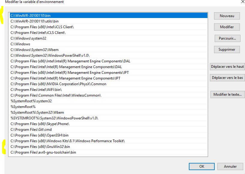
new Path (+WinAvr/Atmel Gnu toolchain and Gnu)
Commands
1. I used Git Bash to generate the .hex file (command "make hex") in the directory of fts_firmware_bdm_v1. Other files are also generated at that step.
2. As I used an usbtiny as programmer I didn't need to edit the Makefile.
3. I then plugged (a bit recklessly) my board in a USB port. The green light lit up. (I accidently inverted the green and the red led while soldering)
4. I connected my board to Thomas's powered programmer with the ribbon cable.
5. Once done the command "make flash" was run. This command erases my microcontroller chip and programs its flash memory with the contents of my .hex file.
6. Then the command "make fuses" is run to set up the 5 working fuses. Based on the reply to the command 3 different fuses are set up (lfuse, hfuse, efuse).
board test
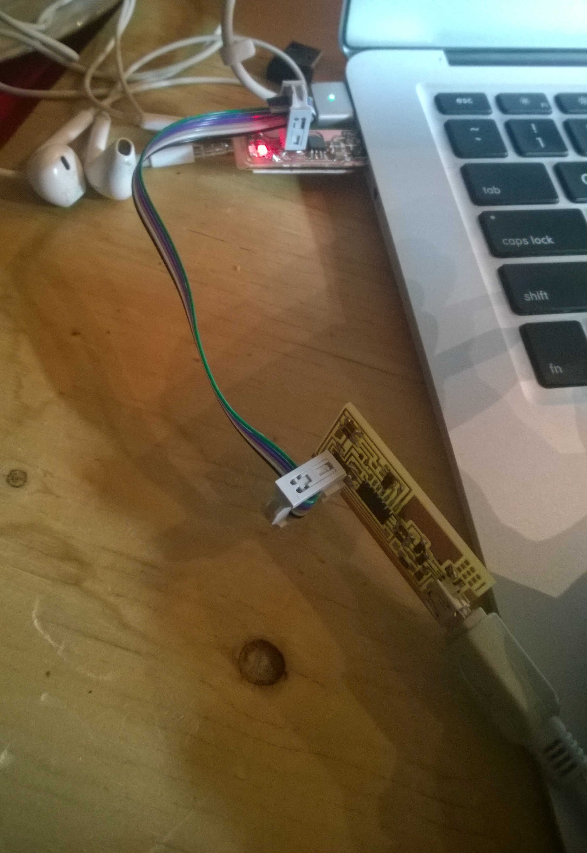
board chain
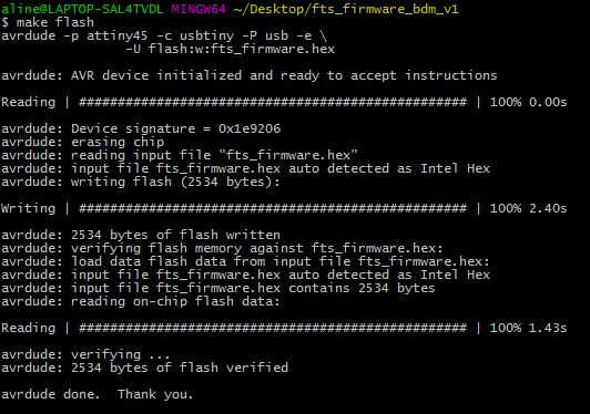
flash instruction
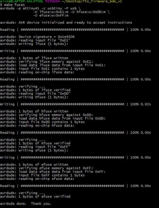
fuse instruction
The command were executed without problem. To double-check the board was unplugged, detached from the programmer then plugged back in. The computer detected it as unknown device.