Abstract
This project is about harnesting mechanical energy.
Some of the question raised were:
- How to minimize the impact?
- How to build something useful?
- How to harnest energy the most efficiently?
-
My biggest achievement:
My biggest struggle:: Keep on believing
Bill of material
Chronology
| January | February | March | April | May | June |
|---|---|---|---|---|---|
| Idea | Technics discovery | Technics discovery | First energy harvesting test | Wifi tests | Project month |
Asssesment validation
They are 5 main criterias of assesment, the project has to:
Then they are deliverables criteria.
First on the Final project webpage does it...
As for the slides, do they include:
As for the video, is it:
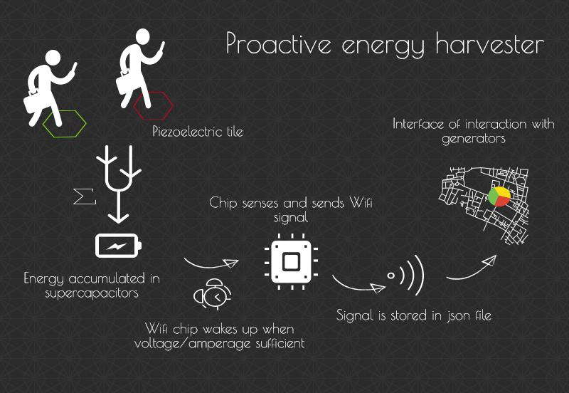
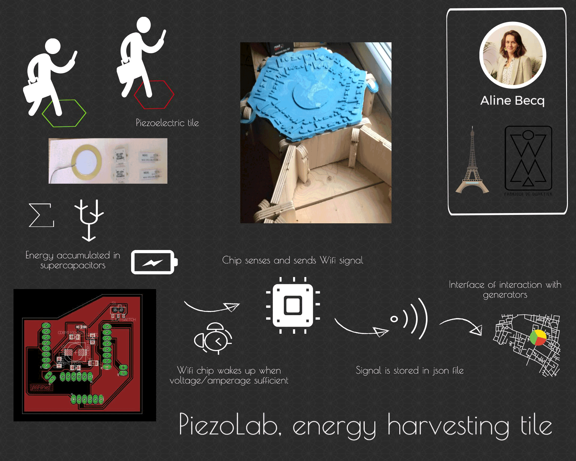
The idea was to build a pavement harnesting energy from bypassers. Several companies furnish those kind of floors, usually the harnested energy is used to generate light. As I wasn't sure I would be able to reach their efficiency in such a short time, I had the idea to first harnest just enough energy to wake up Attiny long enough to sense for example a temperature/VOC and send it as a Wifi signal. The IP will be maped on an interface.
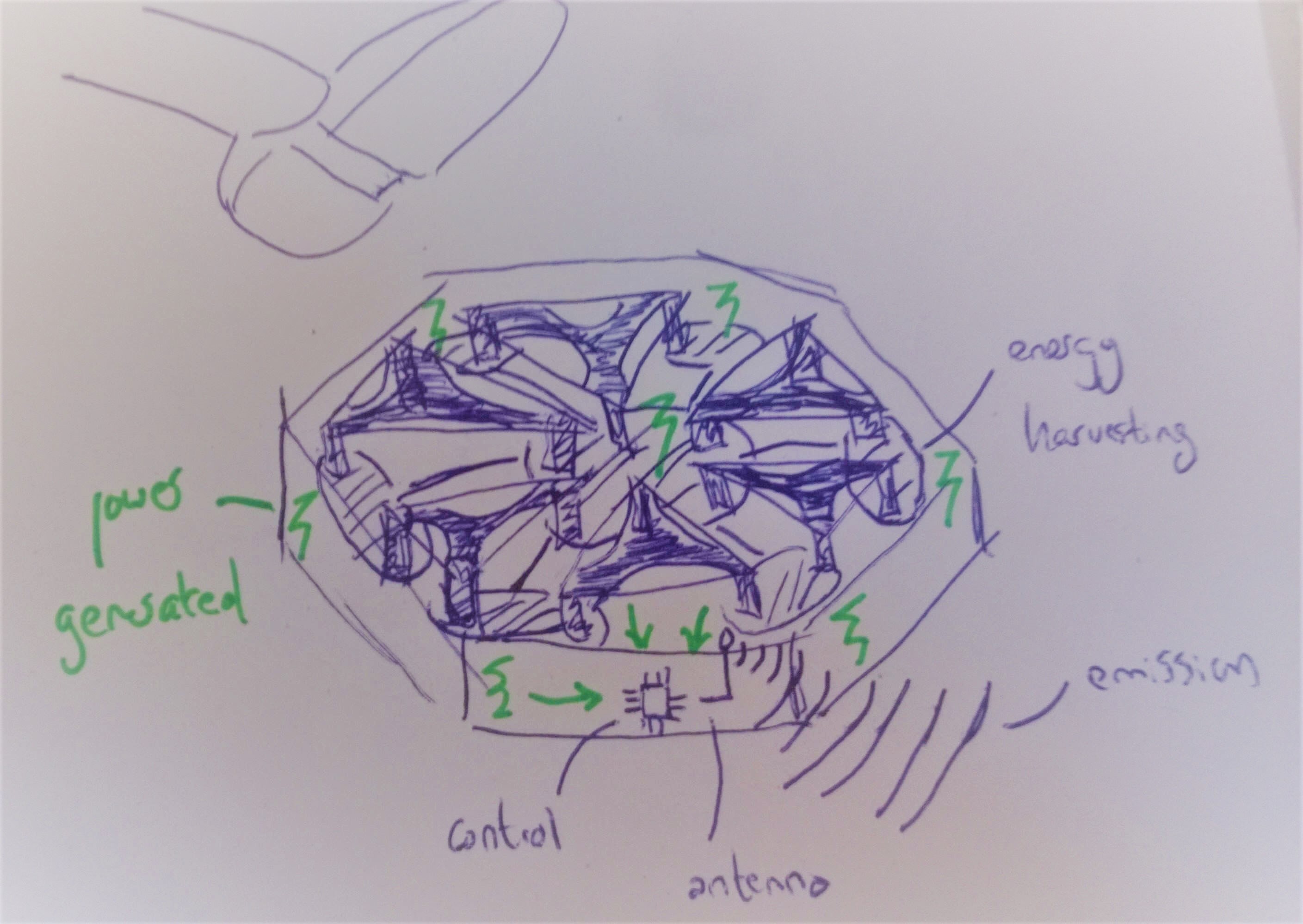
first sketch
the concept
The harnesters would not be MEMS or motor-based to make it cheap but piezo-based. The piezo sensors would be in shape of footprints to involve everyone in the action of sensing. Sensor would not be passive anymore.
To catch up the machine assignement, I wondered if I could not combine both assignements. I imagined a digital enlarger. I used to practice silver photography and appreciate the combinaison of the analog and the digital worlds. So I bought an old enlarger at a photography fair, to repurpose the lenses. I also saw similar project with cheaper lenses.
Here below the poster shown to Neil summrazing my project:
poster
All along the FabAcademy I tried to see how the week could help my project, I usually dedicated a tab for this reflexion. I didn't fill all of those tabs though as I thought added this tab at week 12.
- Week 1 I explained < a href="http://archive.fabacademy.org/archives/2017/woma/students/1/Week12.html#tab4">my first ideas, among them the energy harvesting tiles
- Week 7 helped me think of a mutipurpose design, the hexagonal structure will also be the framework of my pavement
- Week 12's addition to the final project < a href="http://archive.fabacademy.org/archives/2017/woma/students/1/Week12.html#tab4">here
In brief Week 12 helped me to think of a sole, I made a proposition of how to focus force on smaller surfaces through insertion in silicon
- Week 13's addition to the final project < a href="http://archive.fabacademy.org/archives/2017/woma/students/1/Week13.html#tab4">here
In brief I tried to build a capacitive sensor to place below the sole
- Week 15's addition to the final project < a href="http://archive.fabacademy.org/archives/2017/woma/students/1/Week15.html#tab4">here
In brief I build an autonomous Wifi board with input and output
So at the end of the lectures I gathered concepts and could subdivsed the project in layers.
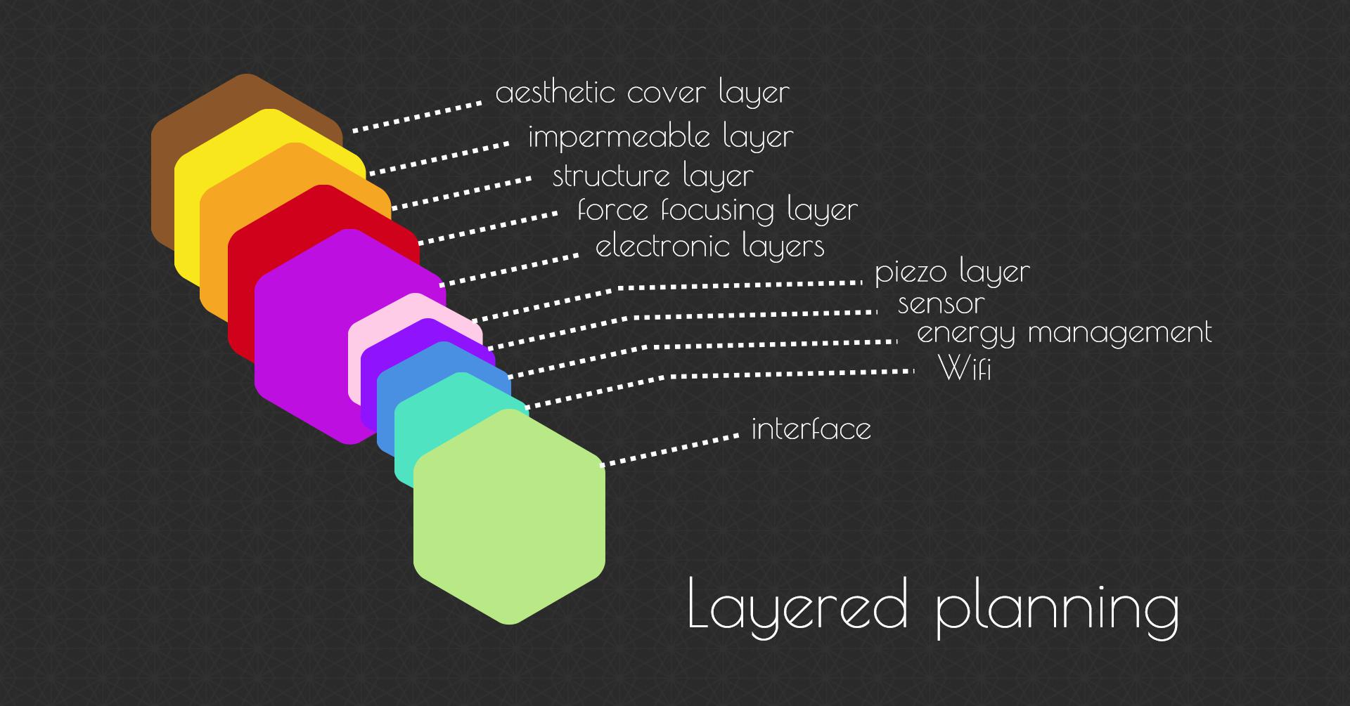
the layers
The layers can of course be combined.
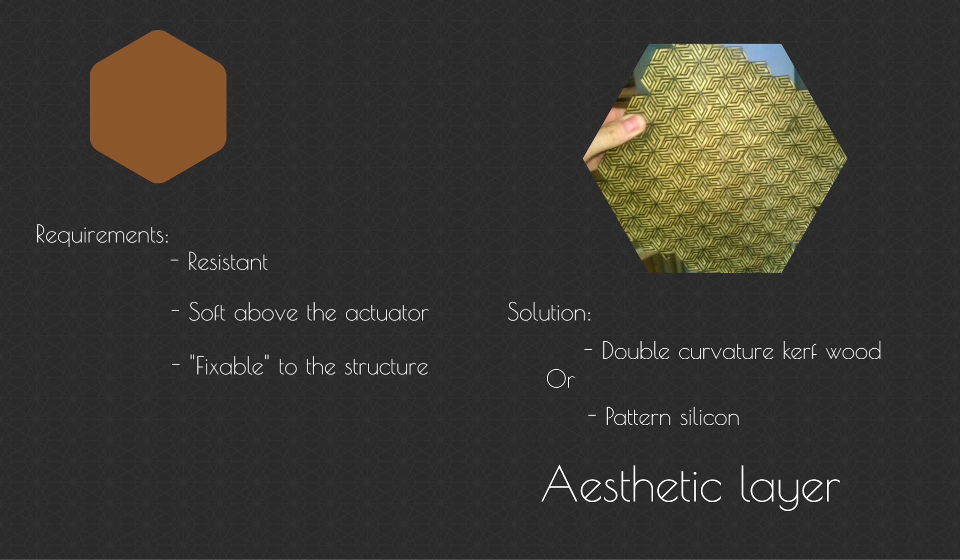
top
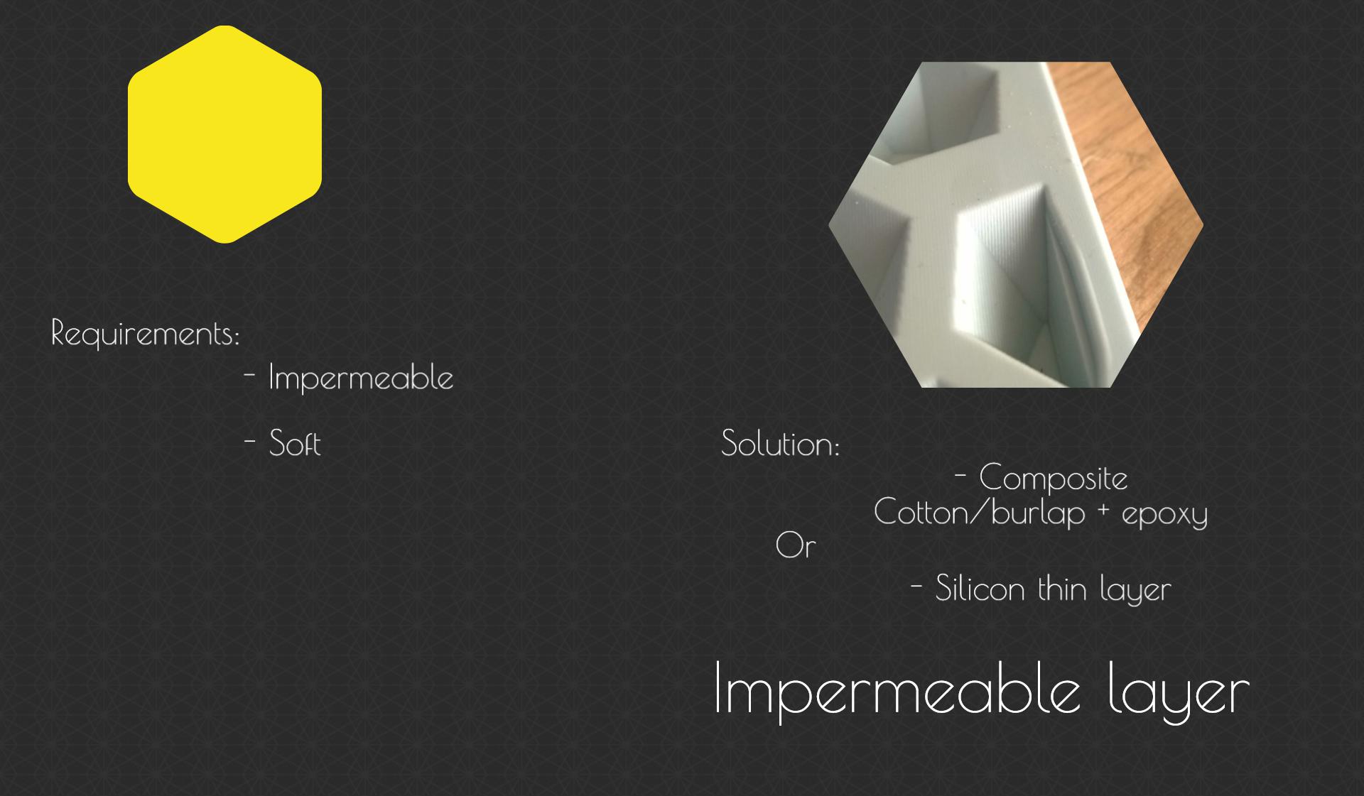
waterproof
silicon
structure
focus
piezo
theory
sensor
electronics
capacitors
diodes
current
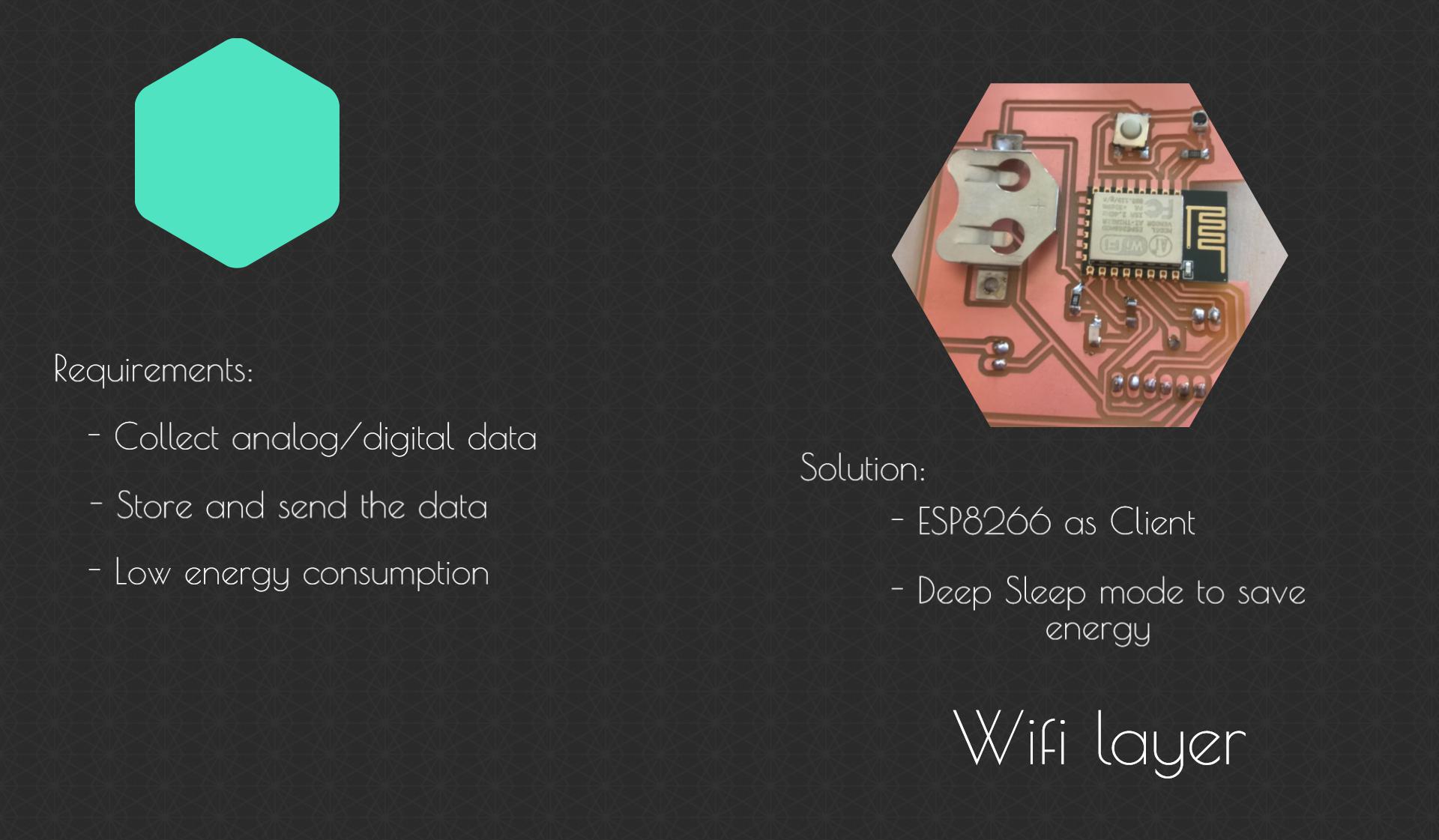
Wifi
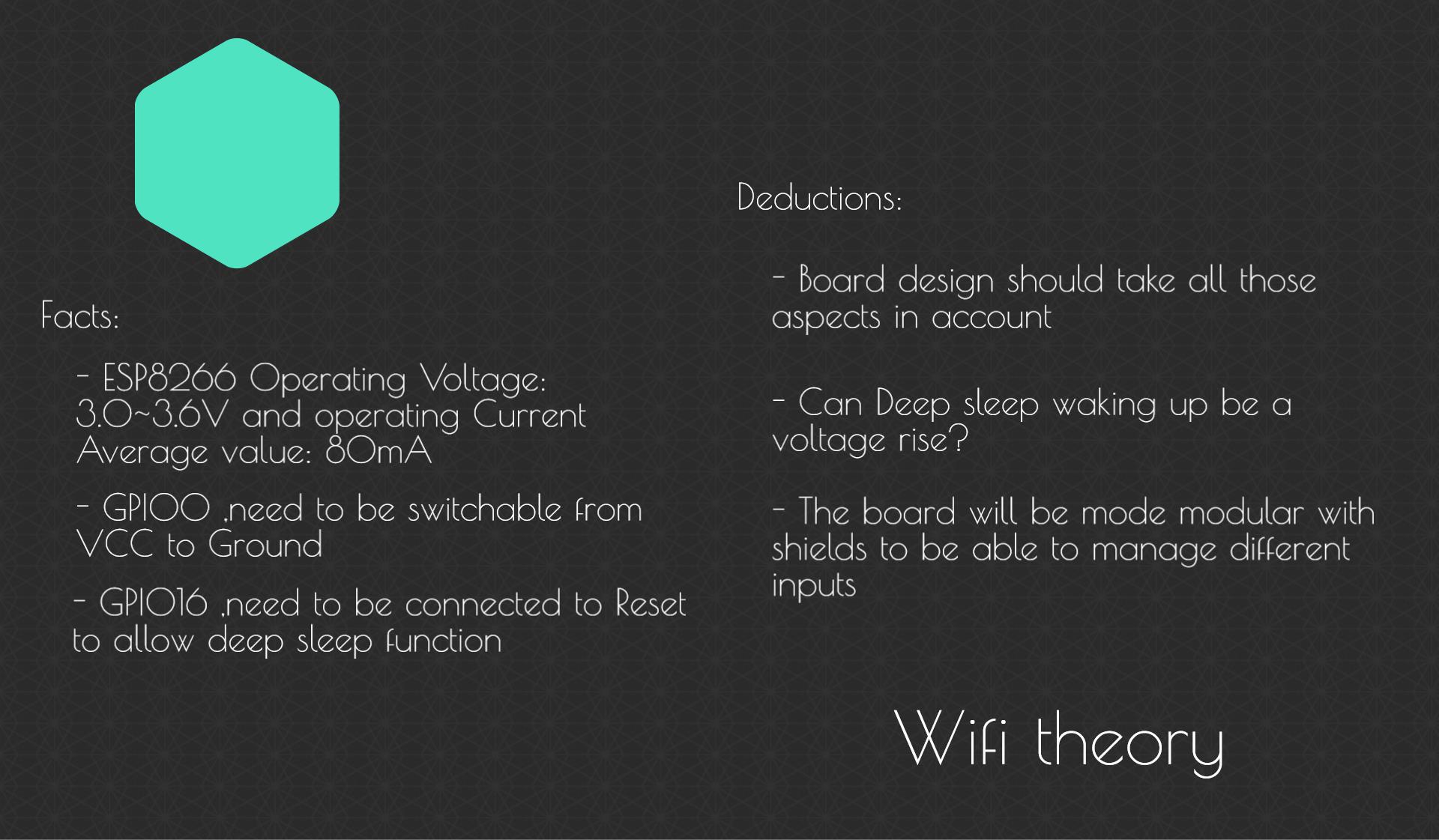
ESP
interface
Arduino IDE
I chose to use Blynk app for the interface as I didn't have a screen. Blynk provides many functionalities and is compatible with Arduino IDE. First I added the Blynk library available in Arduino IDE library manager. Then dowloaded the SimpleTimer library with the Add a zip library functionality.
#define BLYNK_PRINT Serial    // Comment this out to disable prints and save space
#include <ESP8266WiFi.h>
#include <BlynkSimpleEsp8266.h>
#include <SimpleTimer.h>

char auth[] = "084aa63af65649e08c10fdc7e2d31ae2"; //insert here your token generated by Blynk

float voltage;
int voltPin = 17; // ADC pin

SimpleTimer timer;

void setup()
{
  Serial.begin(9600); // See the connection status in Serial Monitor
  Blynk.begin(auth, "Chacha", "7949A964CA6A6F734459ECDC94D61D"); //insert here your SSID and password

  // Setup a function to be called every second
  timer.setInterval(1000L, sendUptime);
}

// This function sends Arduino's up time every second to Virtual Pin (5).
// In the app, Widget's reading frequency should be set to PUSH. This means
// that you define how often to send data to Blynk App.
void sendUptime()
{
  // You can send any value at any time.
  // Please don't send more that 10 values per second.

  Blynk.virtualWrite(10, voltage); // virtual pin 10
}

void loop()
{
  Blynk.run(); // Initiates Blynk
  timer.run(); // Initiates SimpleTimer

   voltage = analogRead(voltPin);
   voltage = voltage * 0.009765625; // costance x10/1024

}
Blynk interface
First I loaded the Blynk app for Android on my phone. Then I created a first project. When the project is created you chose the kind of device you want to connect to it. I chose ESP8266. The network it is connected to is dislayed next to the device name. For each device/project you receive an authorization token via email. This token is an input in the sketch.
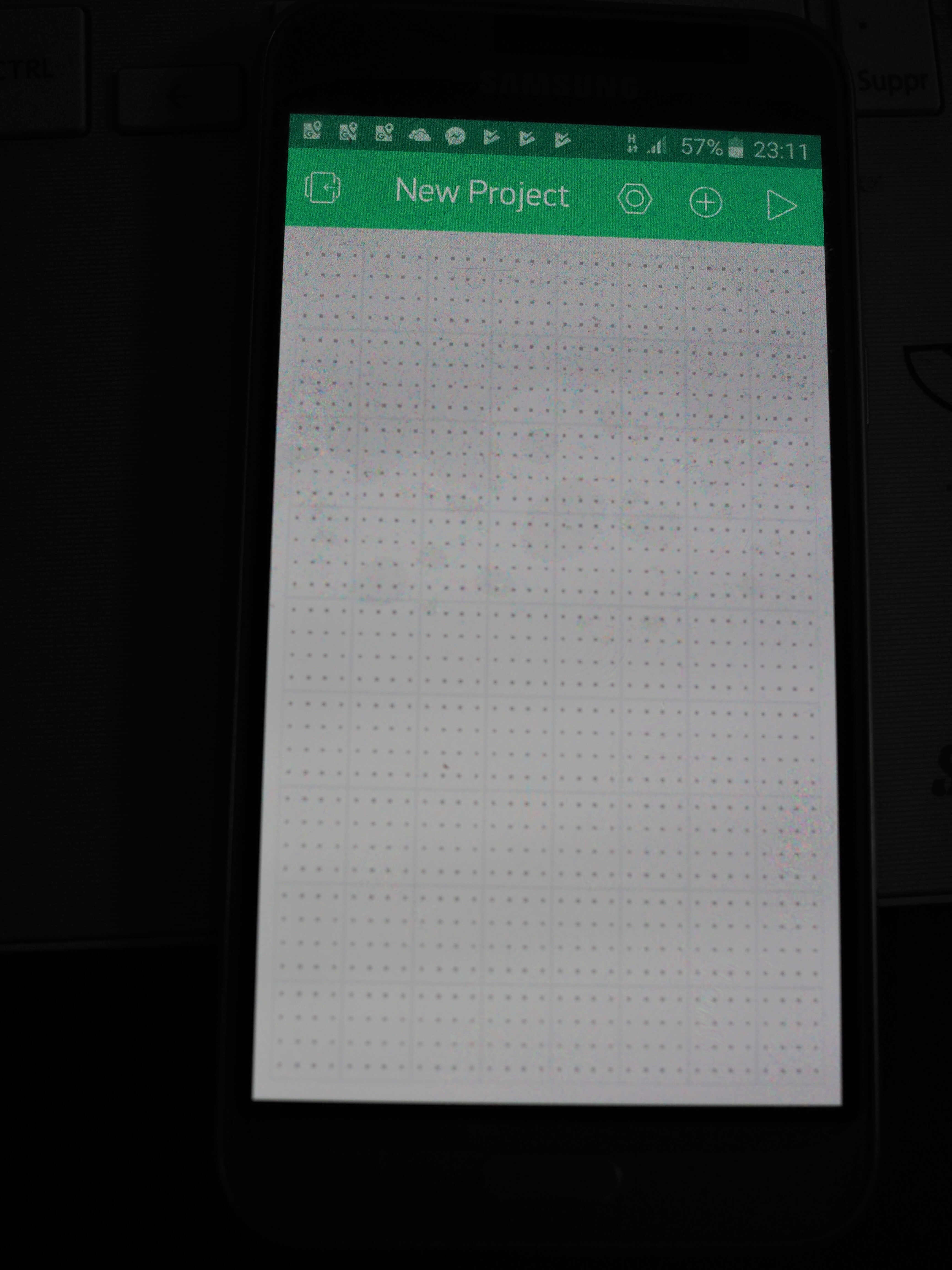
new project
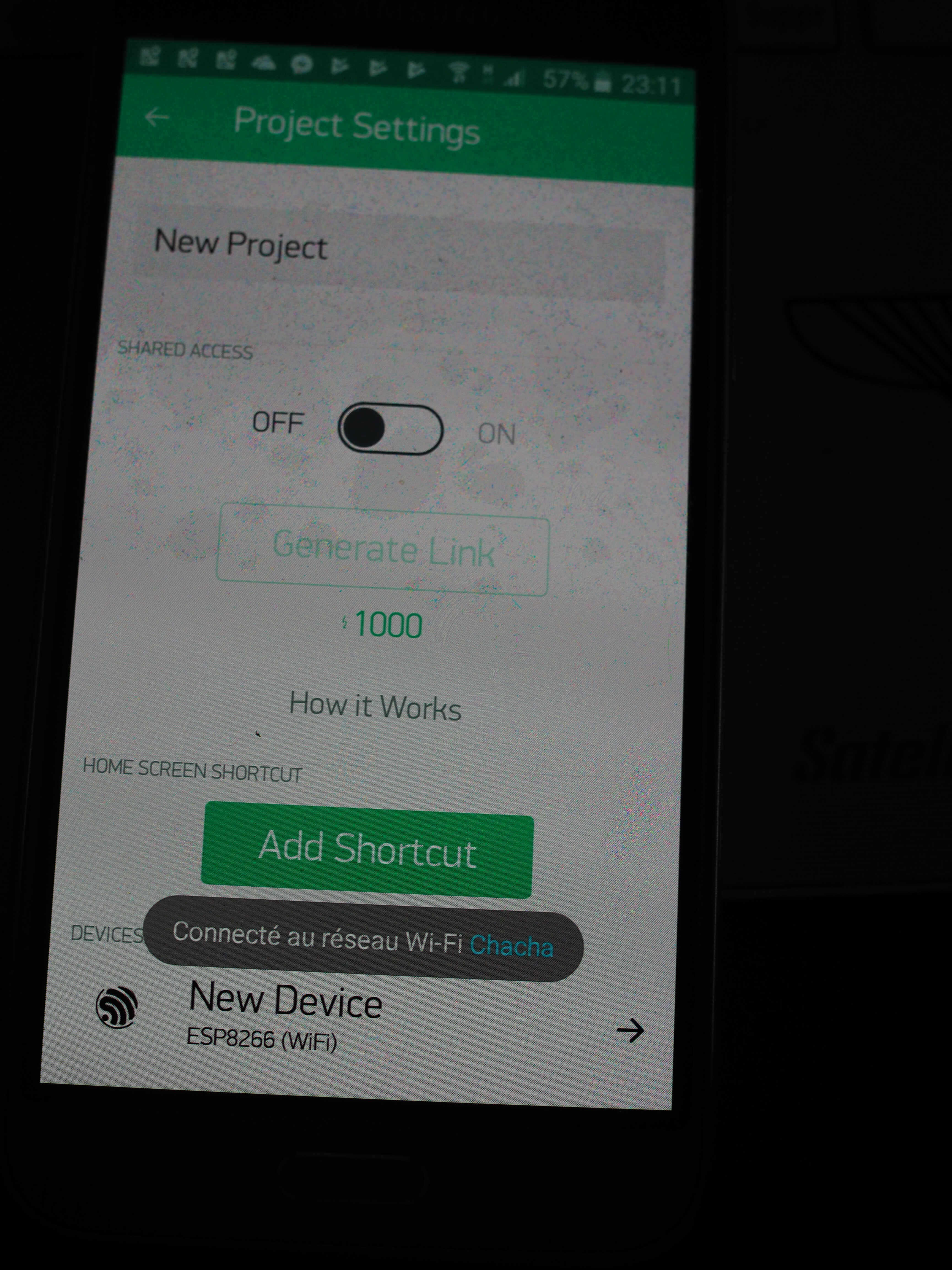
device linkage and connection
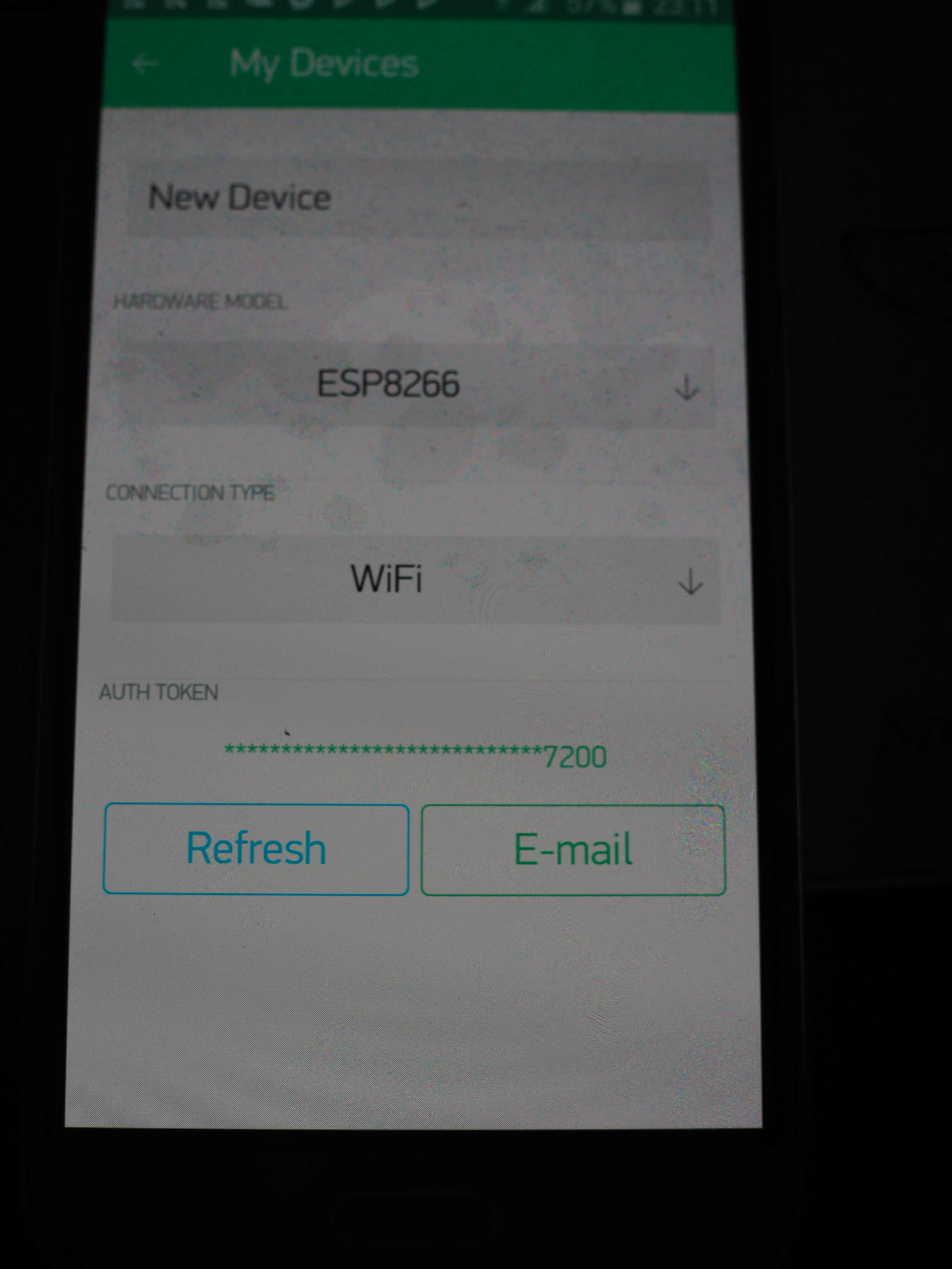
token
Then I added blocks of display or actuators by dragging widget to the main work space. I chose the historical graph as I wanted to follow the signal on long period and to be able to retrieve the data. I selected the ADC0 pin as input. The frequency of the y axis intervals can be adjusted. For other widget such as the gauge the frequency of data retrieval can also be selected. By the way I added a gauge to easily see if a value was read.
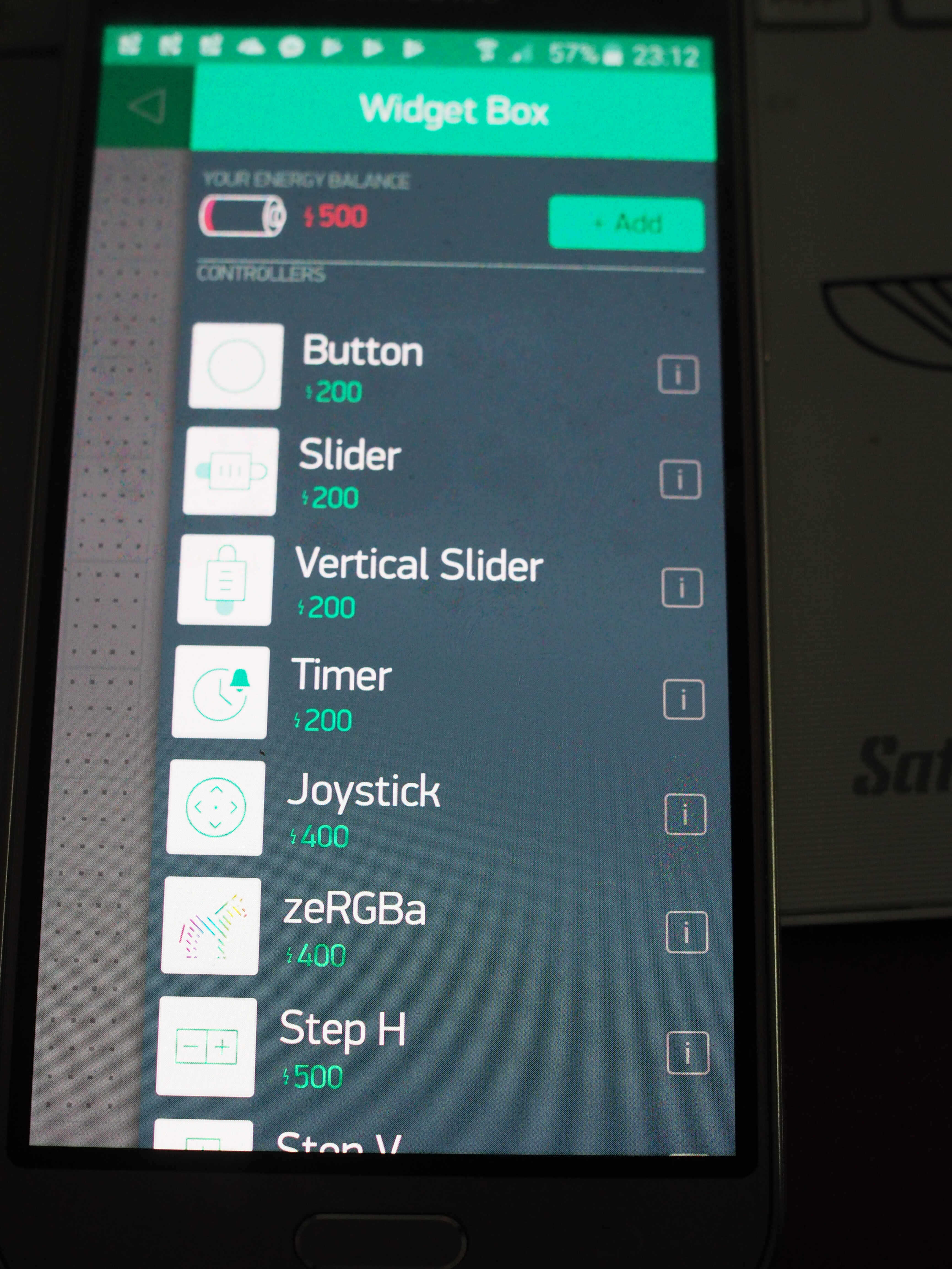
widget blocks
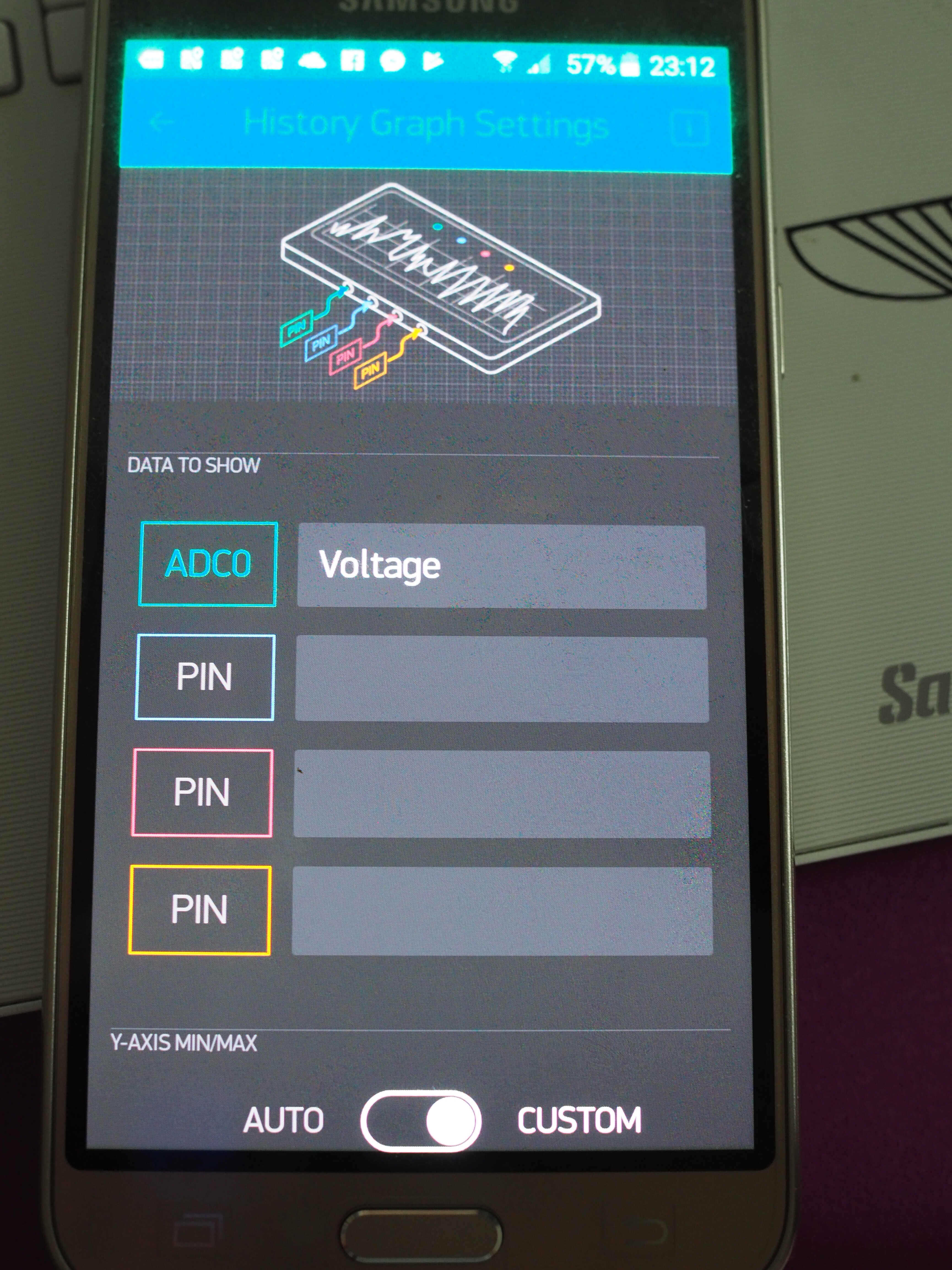
plot selection
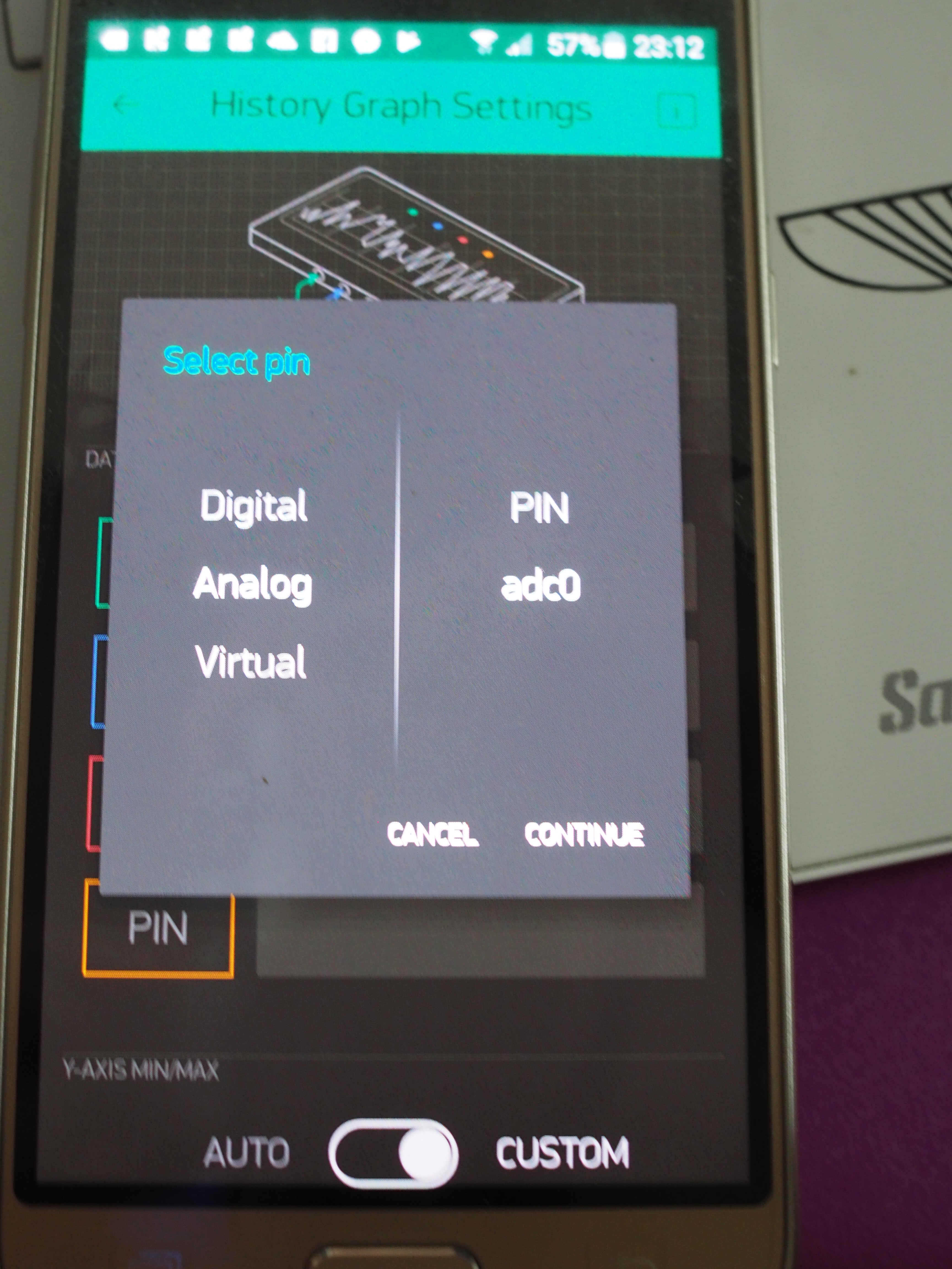
pin selection
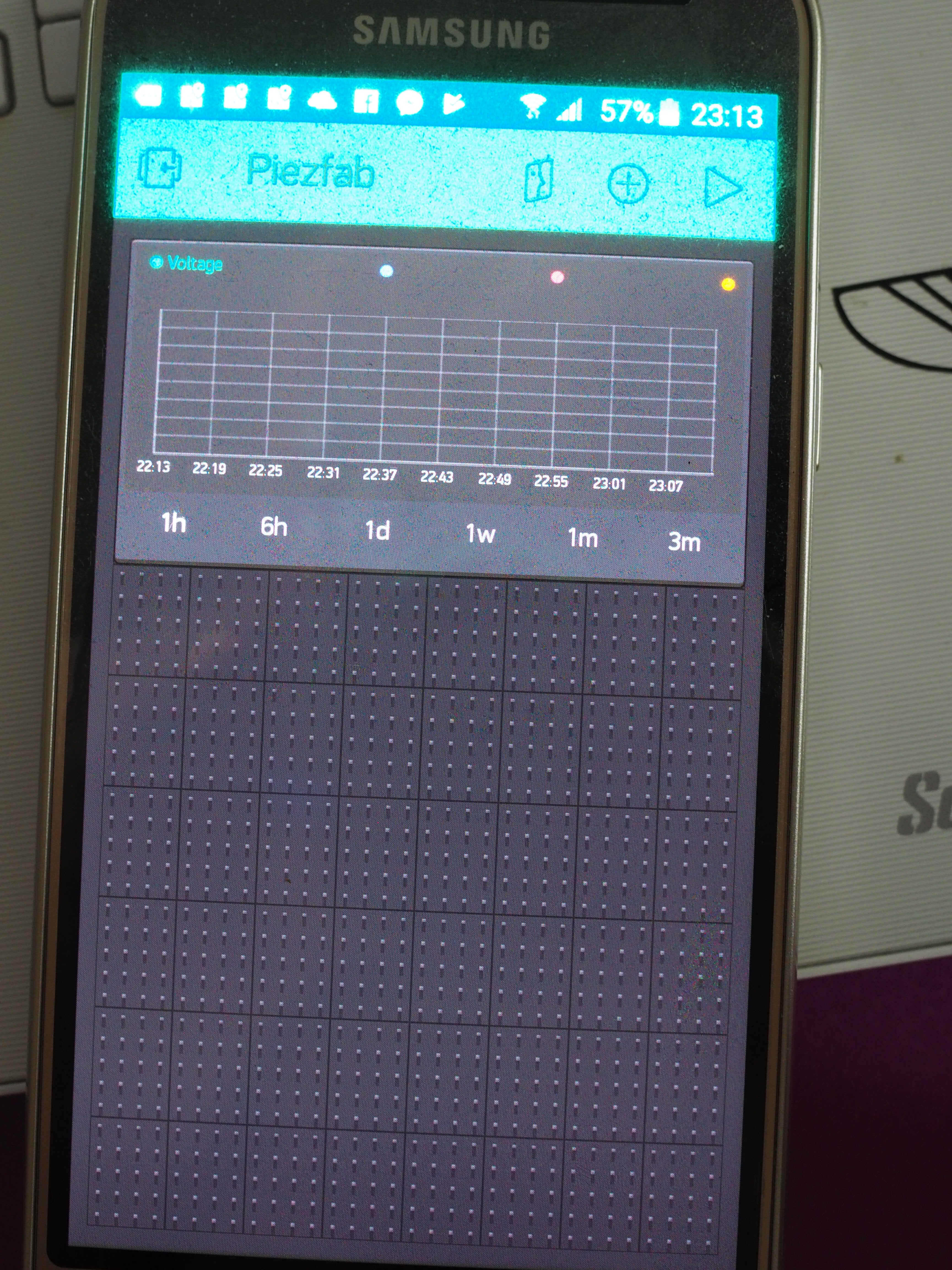
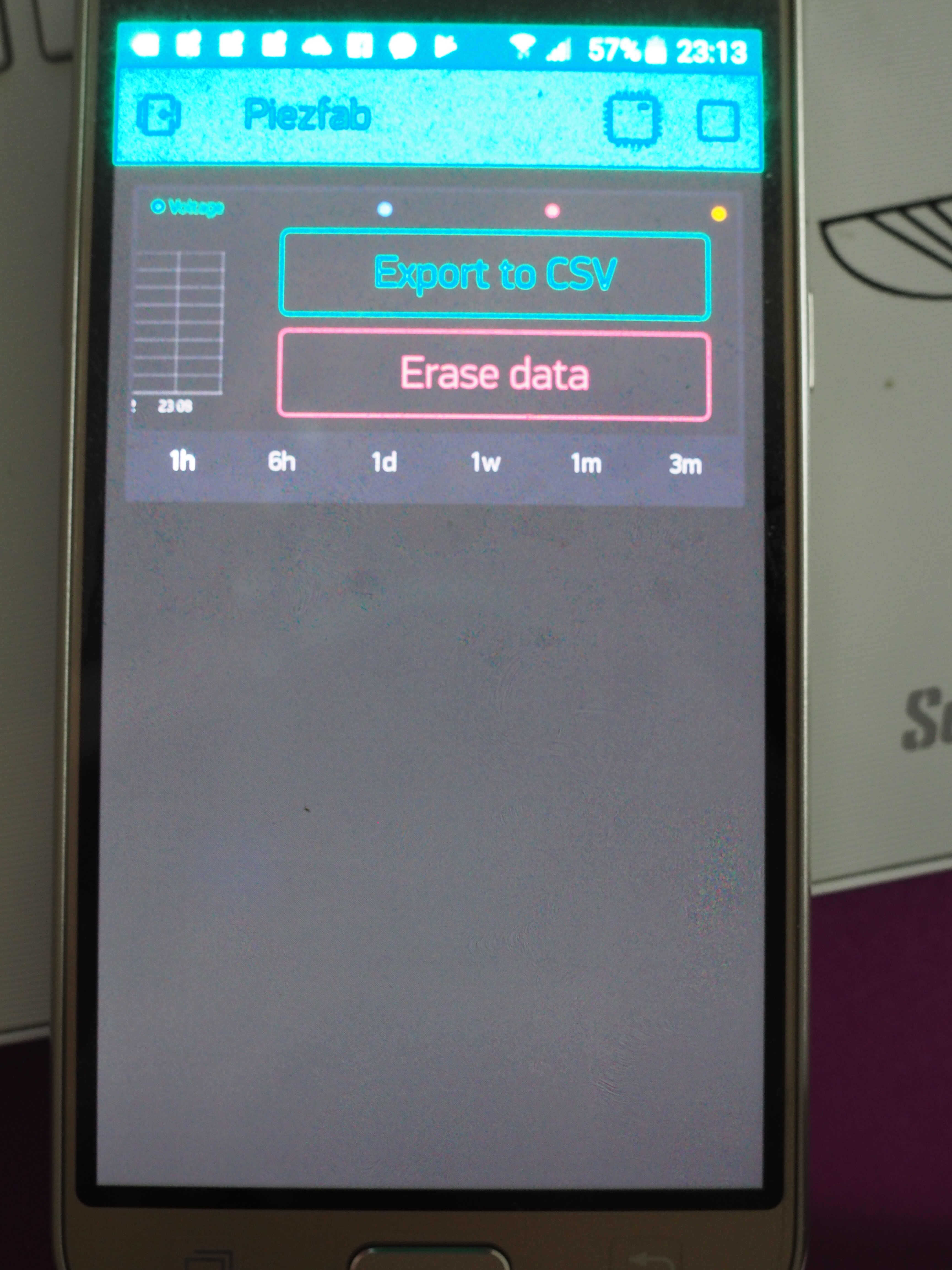
Once done I visualized an empty graph. By swiping to the left the retrieval of the data (in .csv format) is proposed. In the meantime the data is stored on Blynk server. For the project to come to life you have to click on the play icon on the top right.
empty graph
export
I then realized I wasn't using the good pin as my values ranged from 0-1024 and not from 0-12. I should use the virtual pin 10 instead of the ADC0 one as I read in this tutorial on virtual pins. The virtual pin is the one where I did the conversion. Virtual pins are used to communicate between the app and the hardware.
virtual pin
Hardware
I used a breadboard to test this interface. GPIO2, GPIO0, VCC, CH_PD and Reset on VCC GND, GPIO15 on GND I uploaded the sketch then displaced GPIO0 pin wire from GND to VCC. Pressed play on Blynk and tadam. I could play with my array of SMD piezo.
Hardware
Design
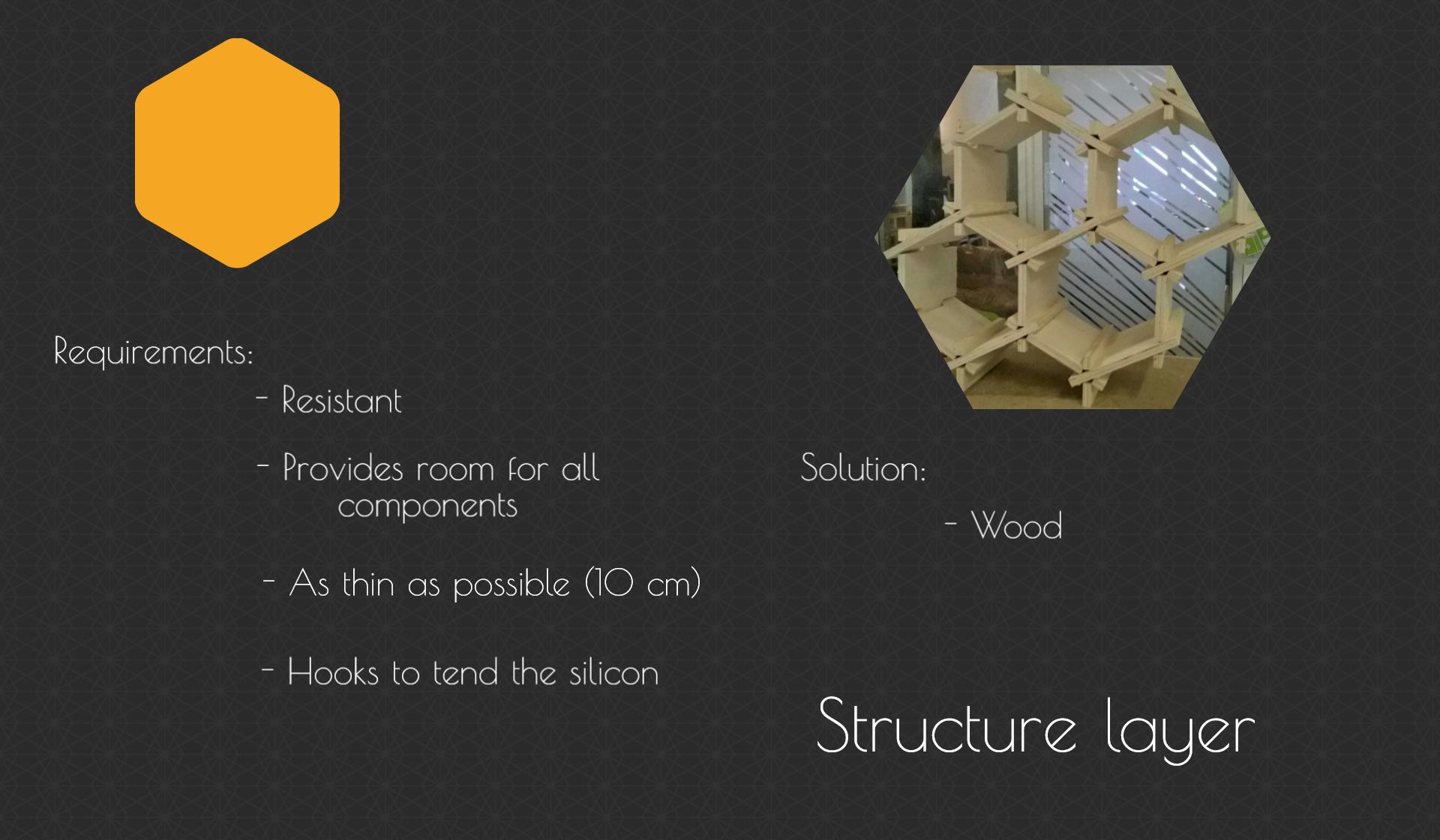
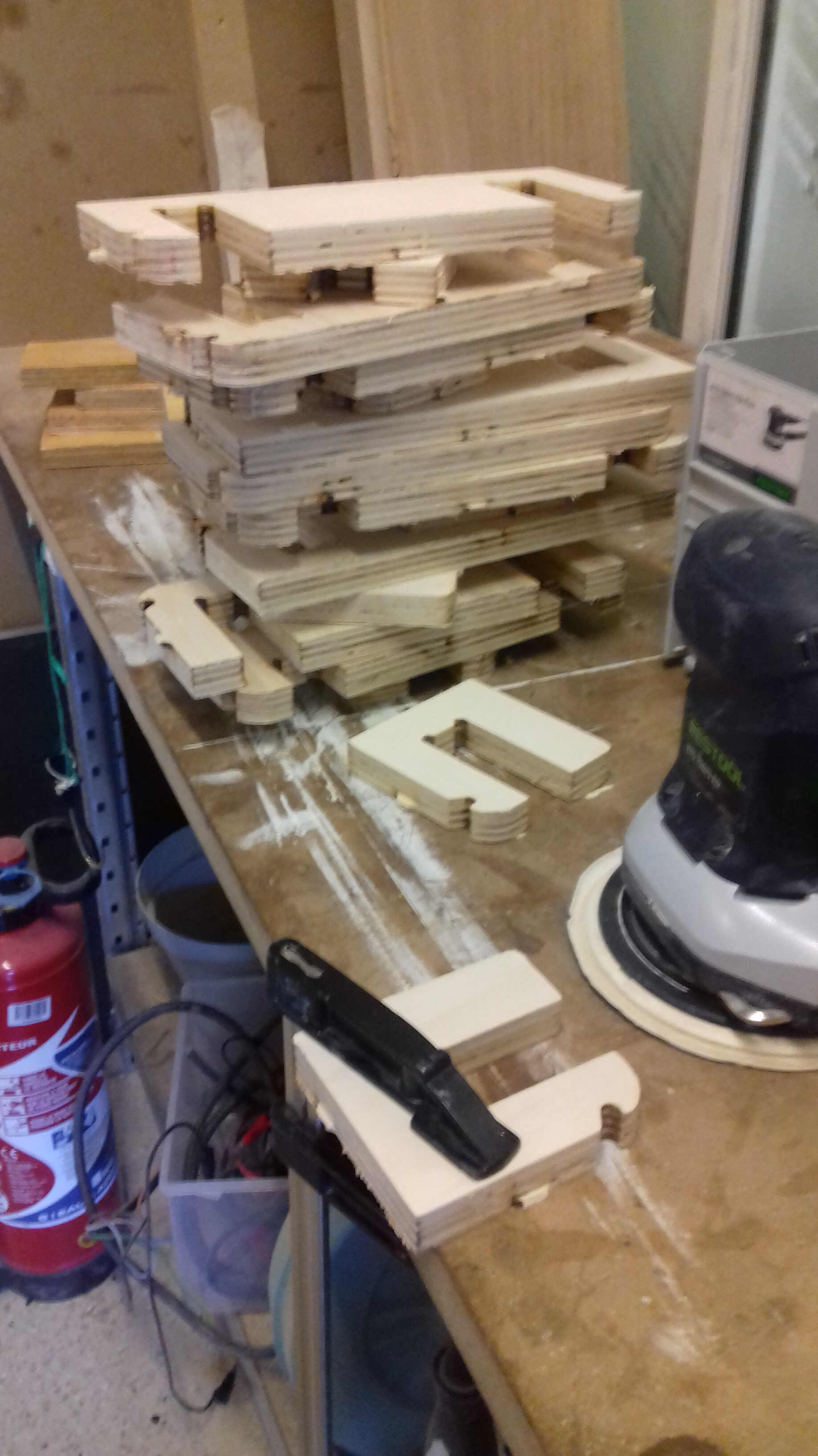
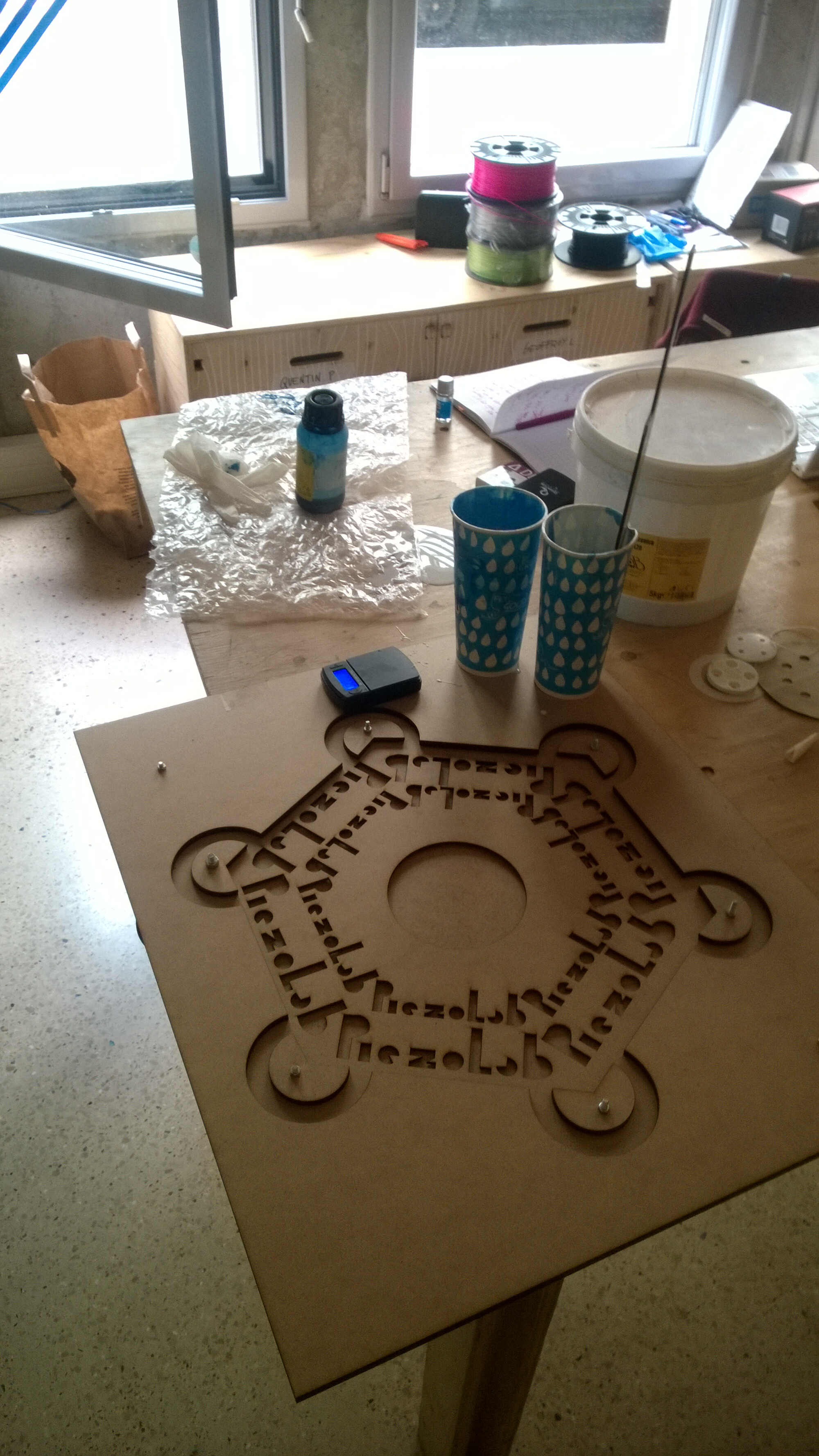
For the structure I reused the Fusion 360 sketches I had for the "Make something big" week. I reduced the thickness to 10 cm, fillteted and added some rounded hooks to fix the covering the external parts. As I struggled with the assembly last time I replaced the rounded slots by rectangular ones. I also slightly increased the slot width.
Source file of the hive furniture to load here
CNC
I faced great issues with the file I exported from Fusion to VCarve. The contours were exploded. The rounded hooks were particularly problematic as I designed them with splines. With Thomas's and Rhino's help we could fix this. I remember facing this issue. I would hence strongly recommend to work with Rhino when designing CNC pieces. As my pieces were smaller than last time, I was advised to add 3 tabs per piece to prevent detachment. I learned how to displace tab to make them more accessible (simple clicking and draging). I used the same setting as last time, the same wood and a 6mm mesh. The file refused to launch as I oriented my panel the wrong way in VCarve. Then everything went smoothly.
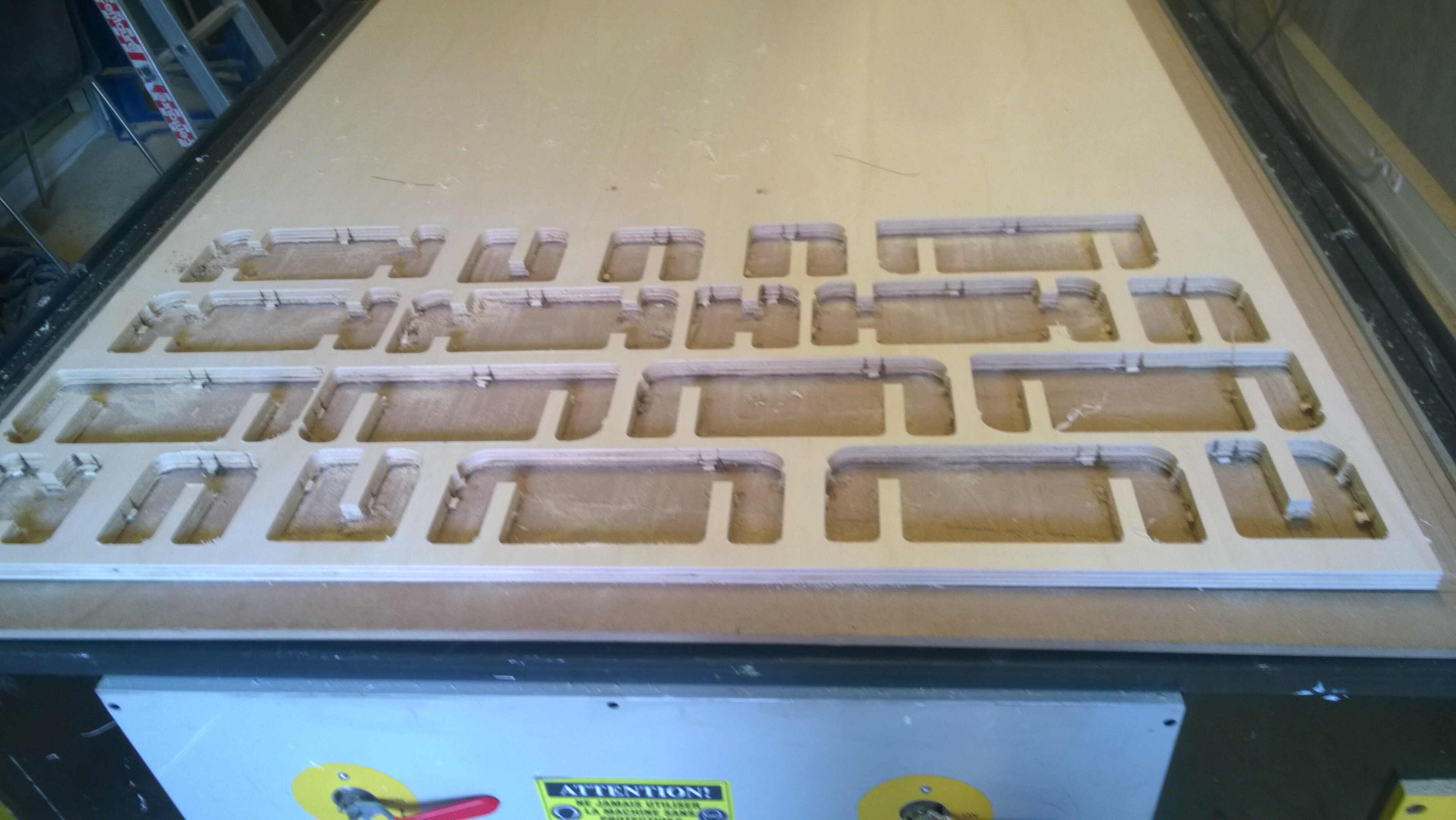
CNCed
Finishing
Once removed the pieces were a bit rough, some tabs remained. I used an electrical sander to fix this.
sandering
I then assembled my structure. The assembly was easier but some pieces were now a bit loose.
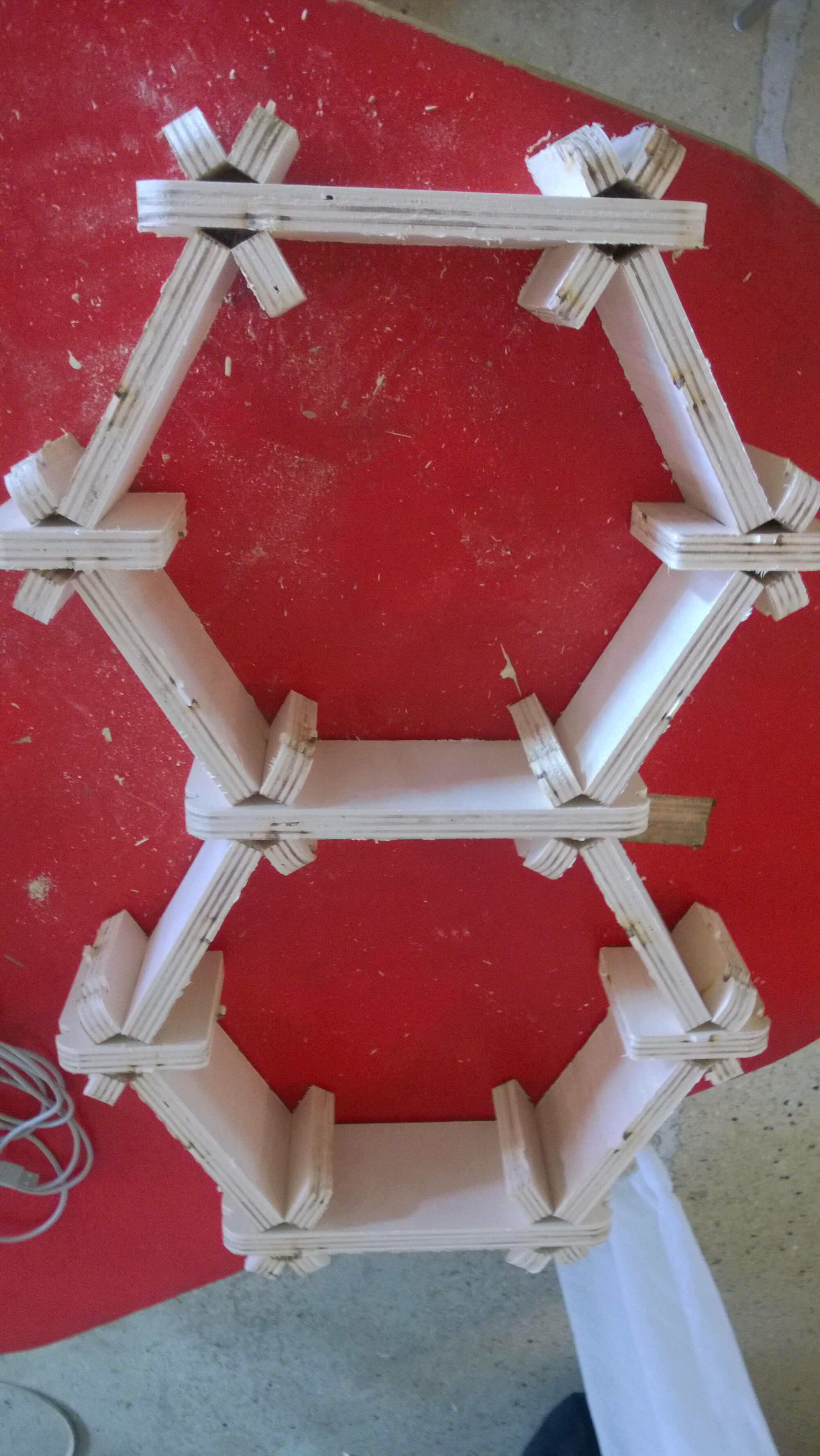
assembly
Tests
I hesitated on the way to make a mold for the silicon. I first considered milling foam, which can be quickly machined. I didn't know how the silicon would react so I made a couple of tests. I used my composite mold depressions for it. I made one with a backing paper on the mold and one without. At the same time I tested different thickness of silicon curing in superposed medium (6-9mm) Those tests showed that the silicon could be poured directly on the foam and as for the thickness both 6 and 9 mm remained flexible. As designing in 2D was easier as well as the access to the laser cutter I went for superposed laser cut medium. I picked a total 9 mm thickness (6 mm base, 3mm relief). Those tests allowed me to measure the elongation of the material (118%).
foam + paper
direct foam
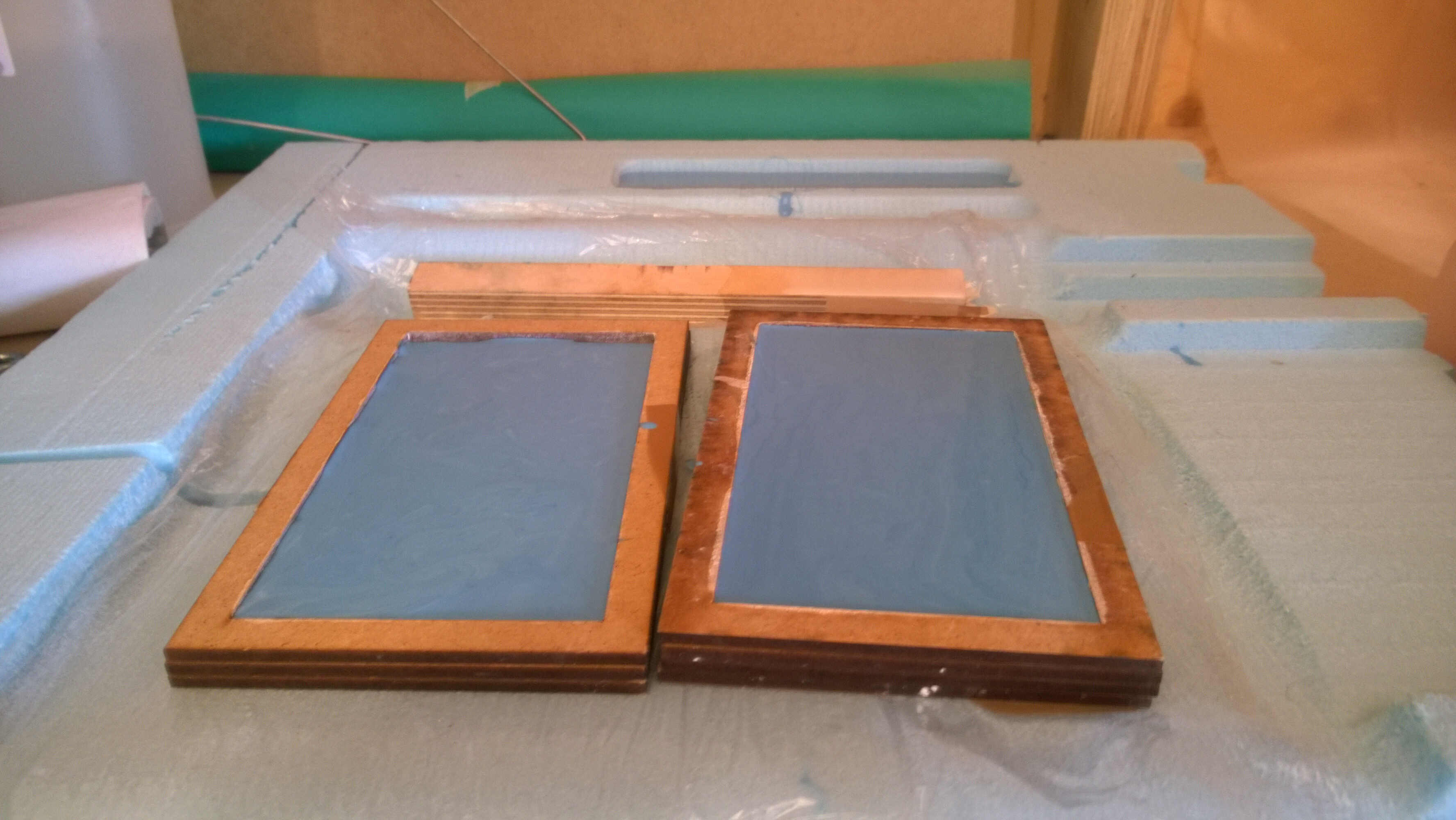
thickness + medium
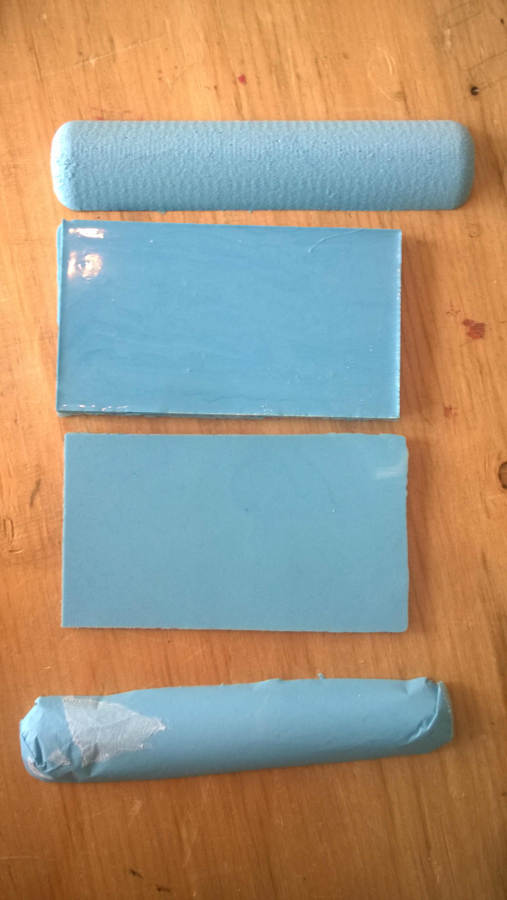
test result
Design
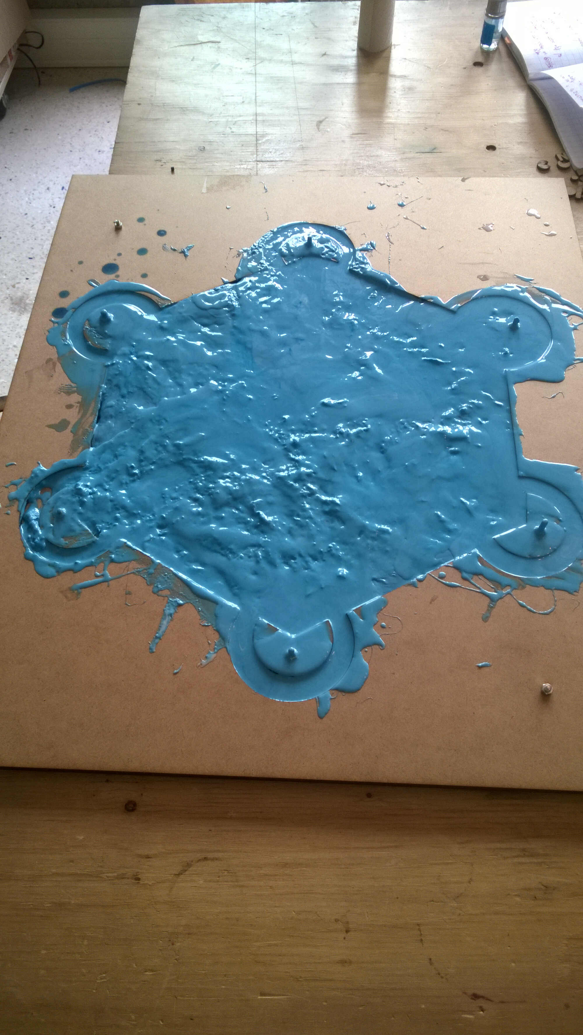
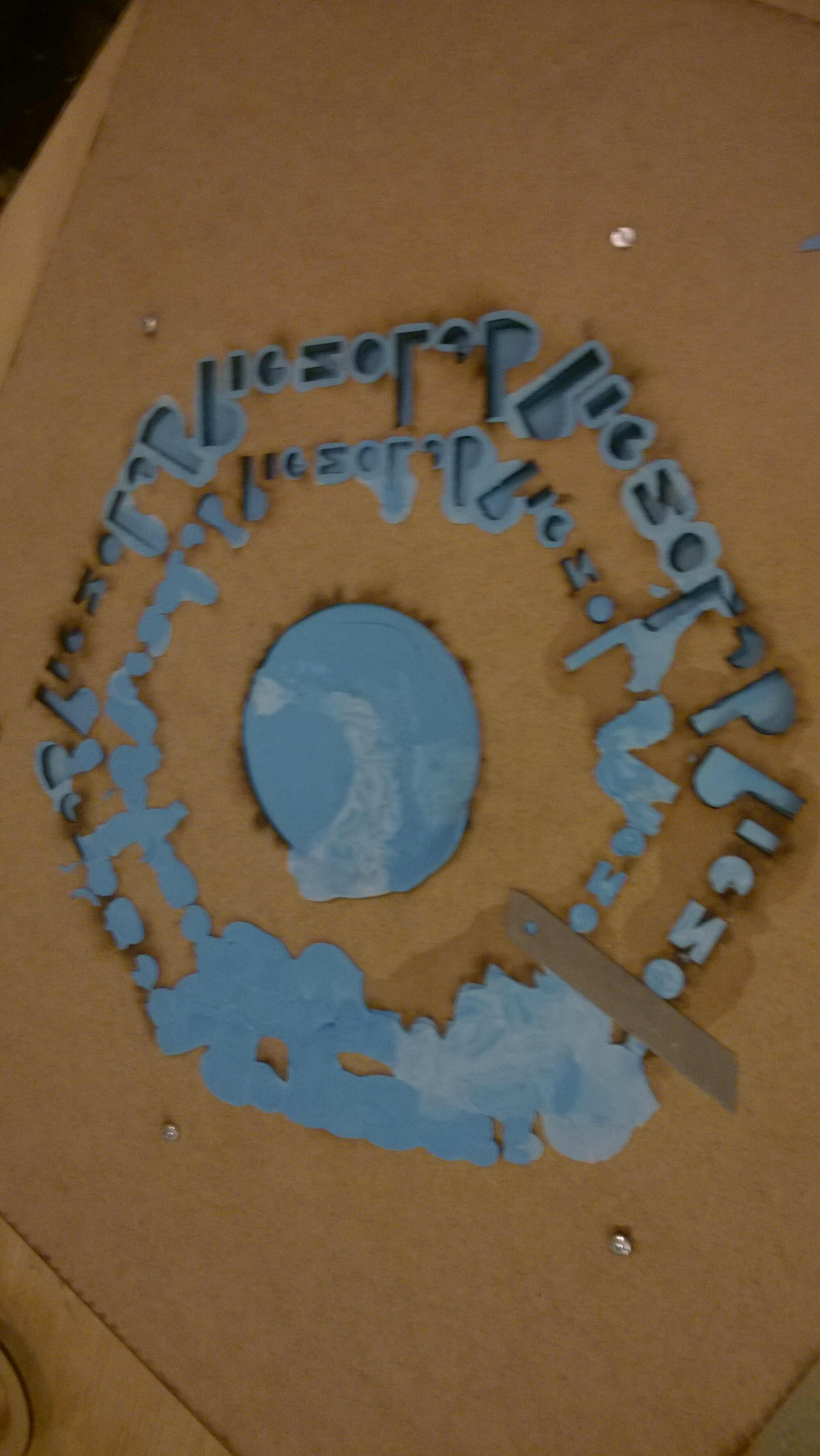
The silicon covering was designed in 2D in Fusion 360, the third dimension emerging from the superposition of layers. The first layer was a relief layer where I wrote the name of the project multiple times (PiezoLab) and at the center I added a central pad. This would have a non-slip function. The second and the third layer would make the body and the coves. I struggled to design those. The can be seen in the fact that I forgot to mirror the names. To get this result I used the Combine and the Project tools. To get the outline I assembled my structure in 3D and used it to sketch from above. To design the coves I took the elongation into account so that once fixed the slicon would be tensed. A fourth layer was designed to be used as base. To make the superposition easier holes across the four layers were added.
Source file of the mold furniture to load here
CNC
Once the 3 layers designed they were cut with the laser in 3mm thick medium planks (Power: 60, speed: 1800). At the end they were assembled with bolts and screws.
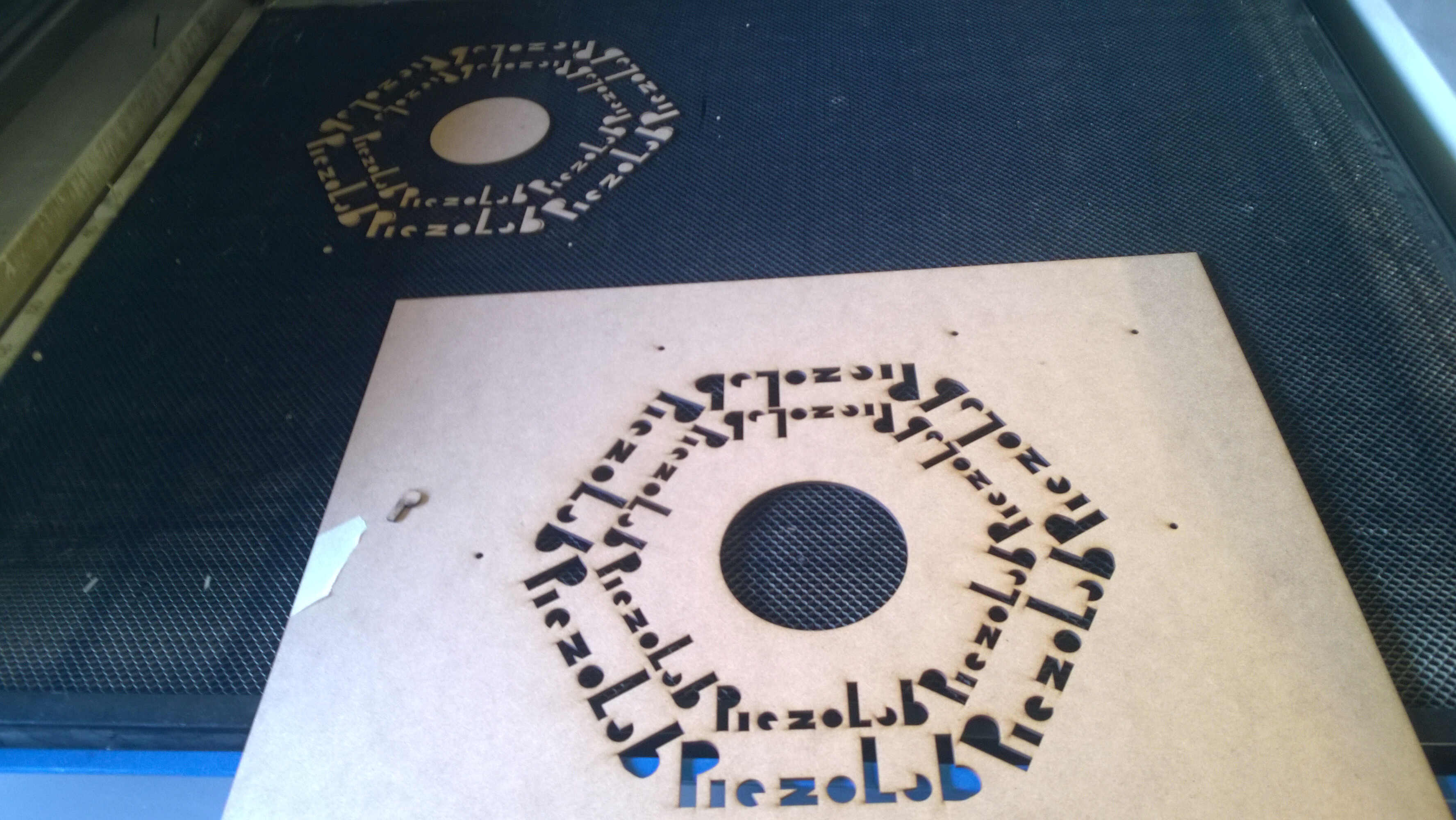
laser relief
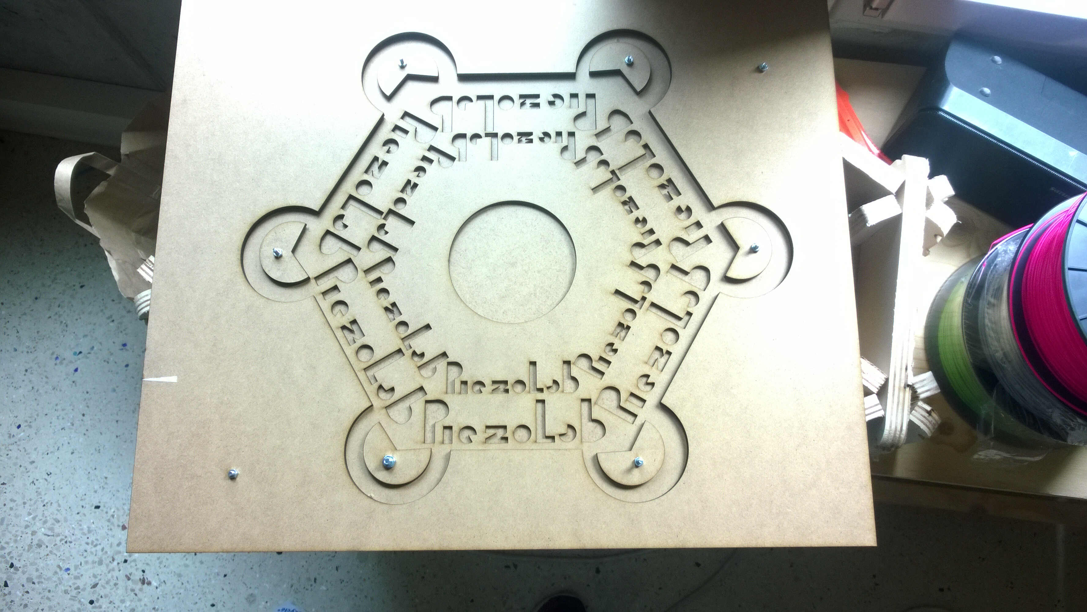
assembled mold
Molding
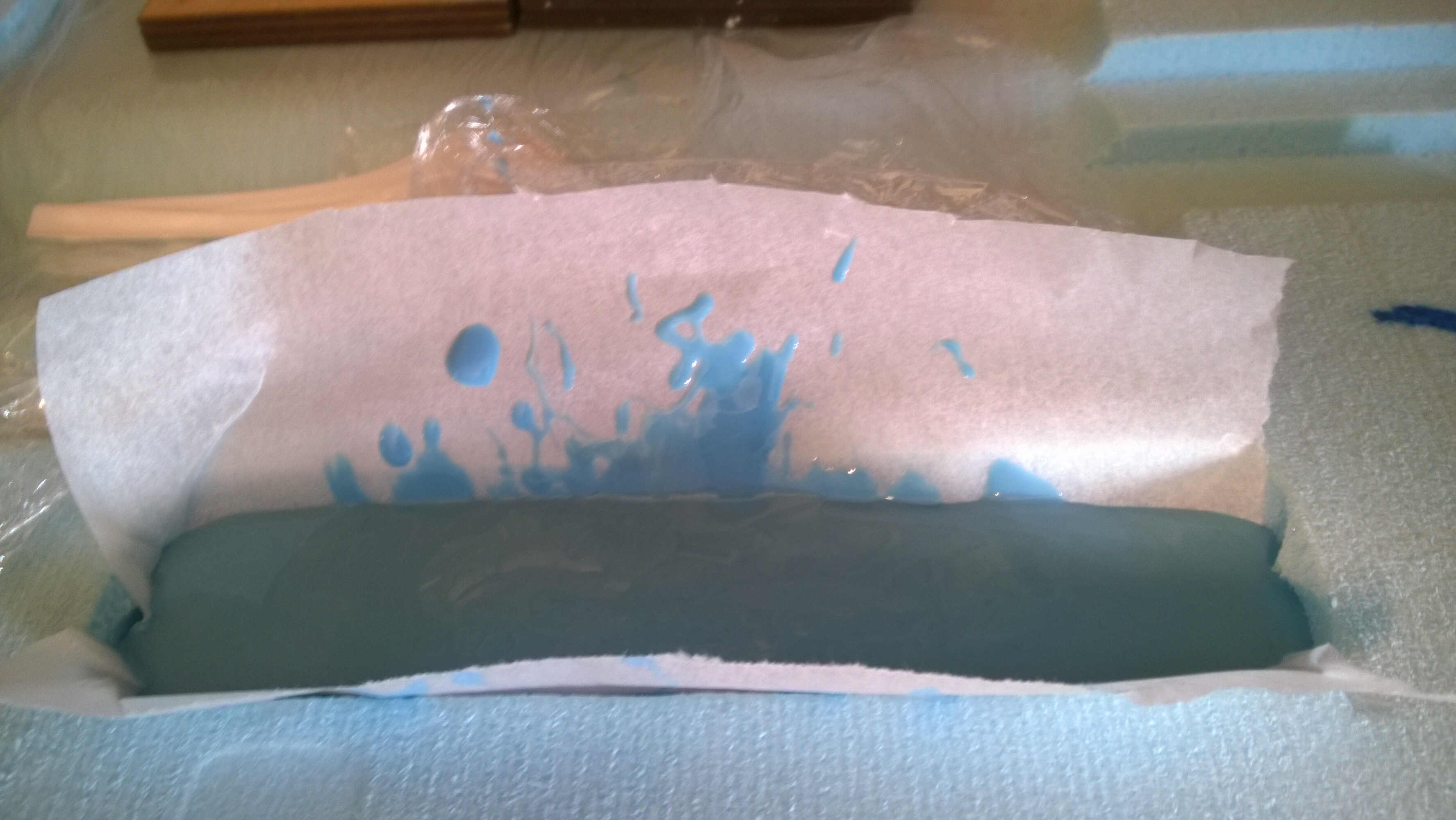
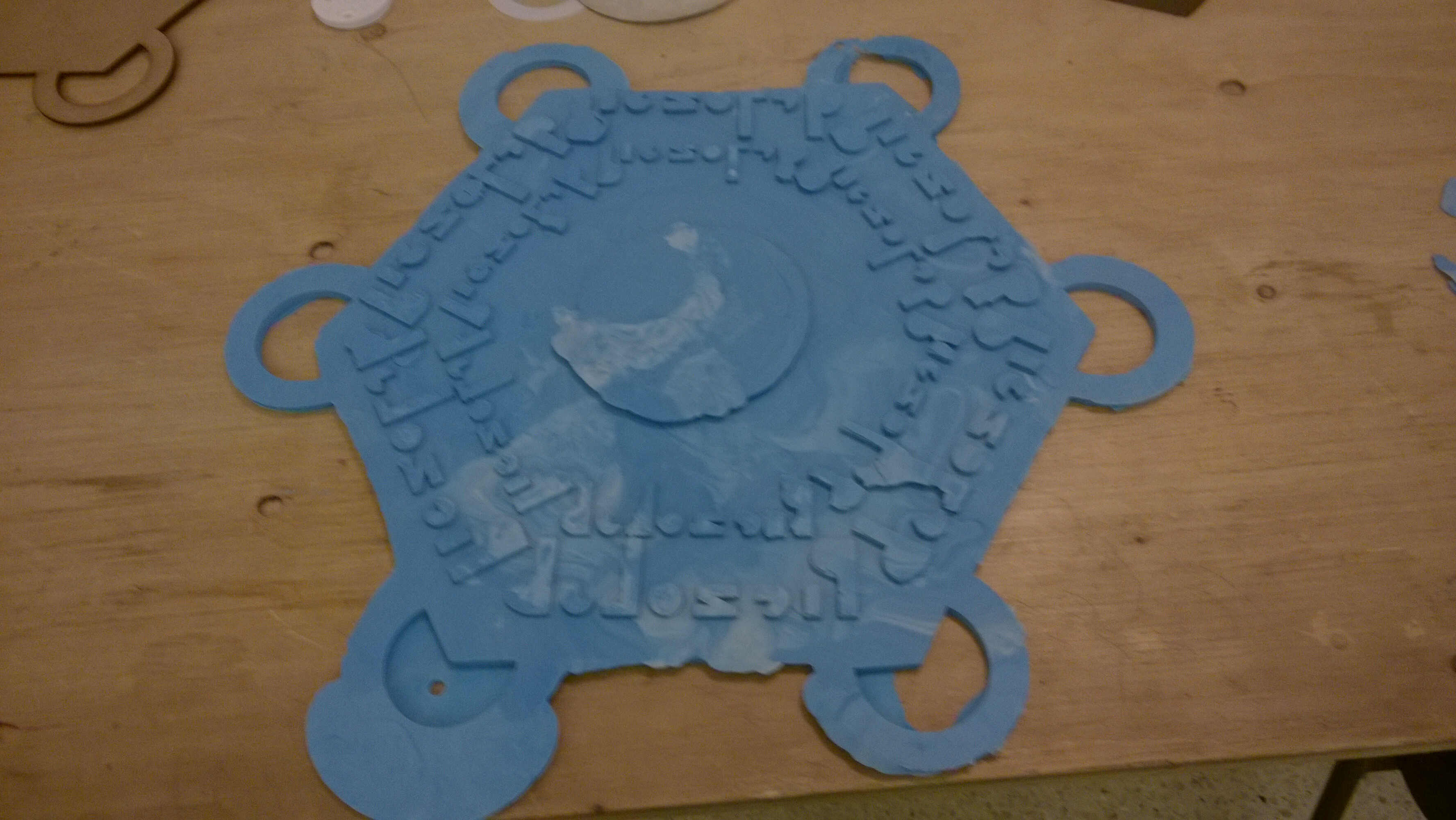
I used my sketches to get the volume of silicon needed. I reached 679 cm3 (300 per base layer and 80 for the letters). As my cup measured 620ml I decided to miw 1 cup filled at 3/4 and one at half. This should have given me 775 cm3. I was difficult to mix such quantities, the first cup started to cure before I poured. This biaised the volume. The heterogeneity can be seen in the covering final colour. I ended up being short of silicon and the pot was empty. Due to this 1 cove was partial.
setting
pouring
Demolding
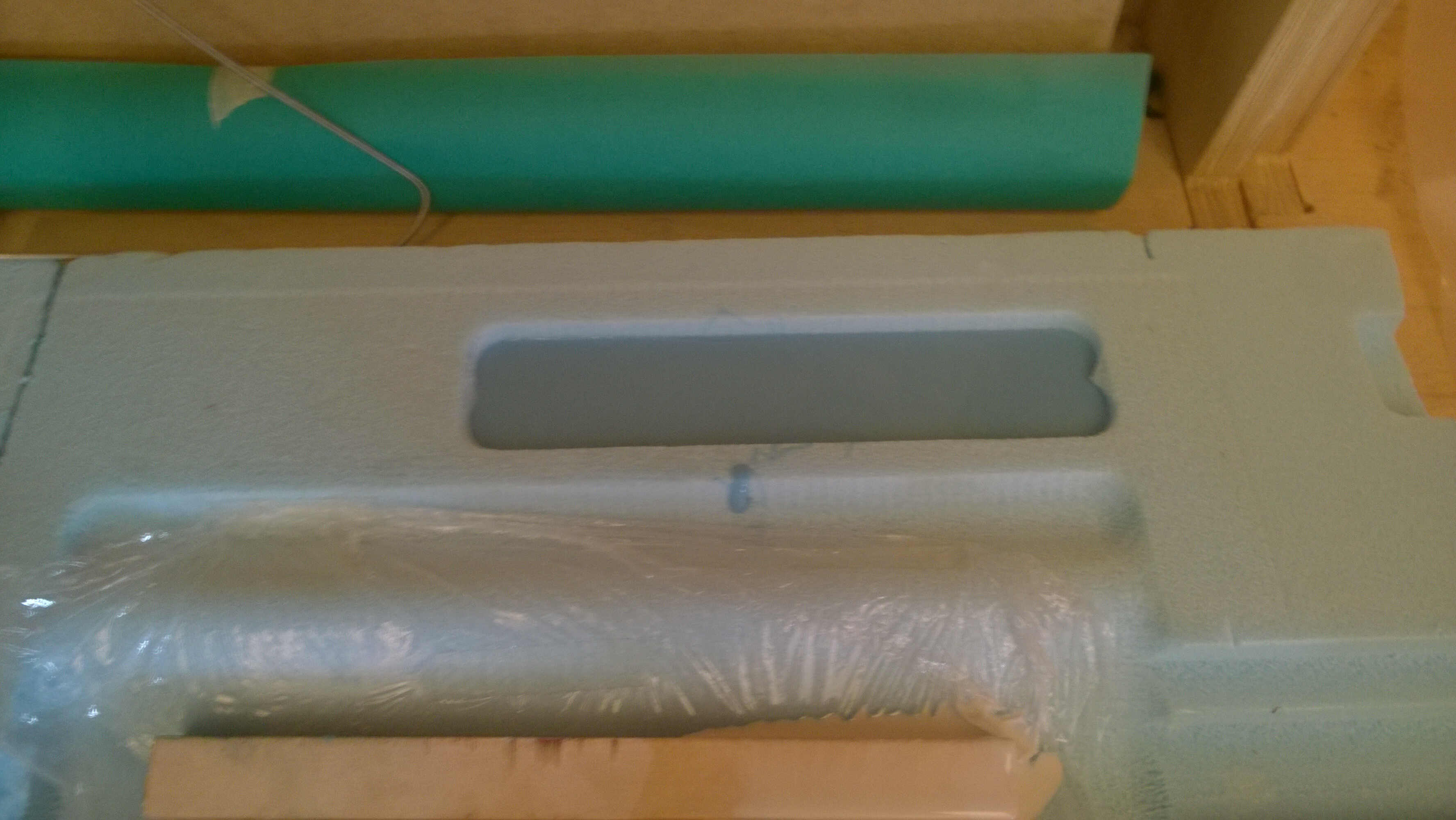
I demolded after only 4 hours because I wanted something to show in my video. It was quite dry. I tried to unmold from above, it caused some tearings as the 2 bottom layers were not tight enough and some silicon overflew. I then unscrew the layers and removed one after the other. The demolding was quite satisfactory. The behaviour of the silicon the one I expected. The major improvement that could be made would be to make the holes of the coves circular because mine have sharp angles. Those angles focus the force and cause tearings. To clean the silicon I used a cutter.
spilled silicon
demolded
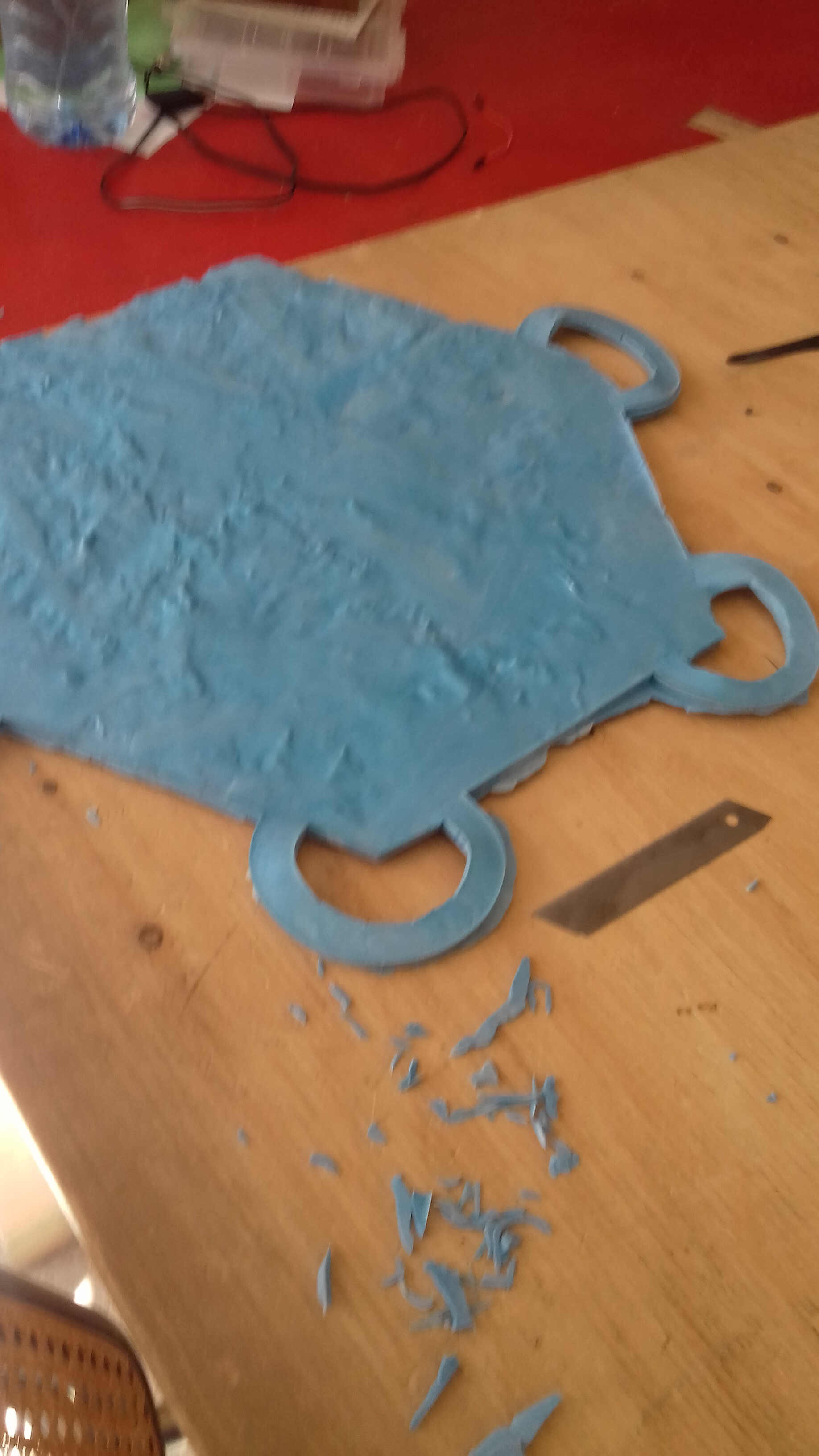
fixing the spil
The electronical part was the most time consuming. The first objective was to power an ESP with a piezo tile. As the amperage remained low despite several tries I reoriented the project. I decided to build the first project on the road to self sufficient ESP. My board would now measure the voltage to see if we can maintain power long enough for the ESP to work and sense.
Tests
For 2 weeks the board CNC was down so I had to test as I could. For the group project I designed a small rectifier linked to a led. I used this to test my arrays.
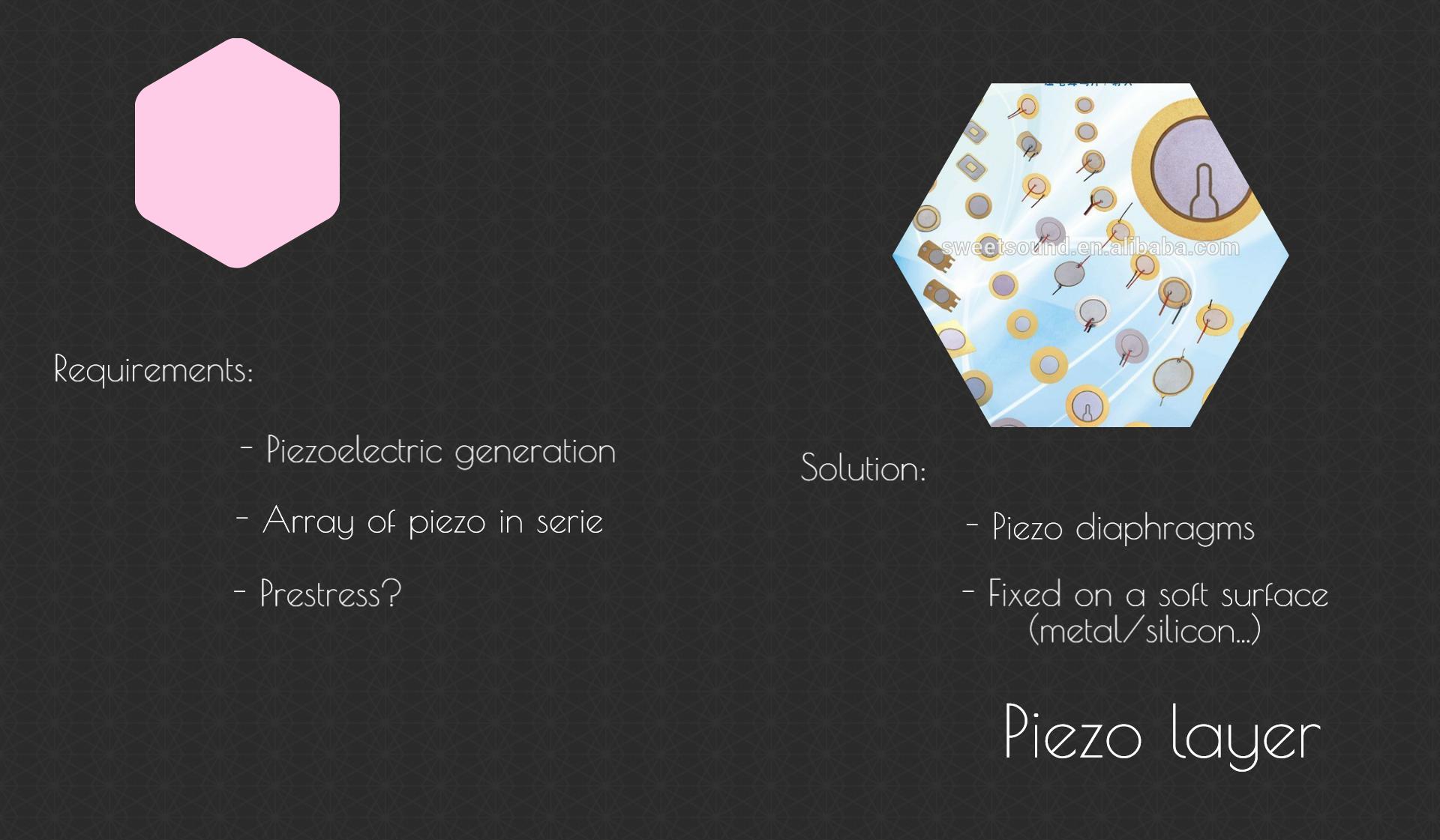
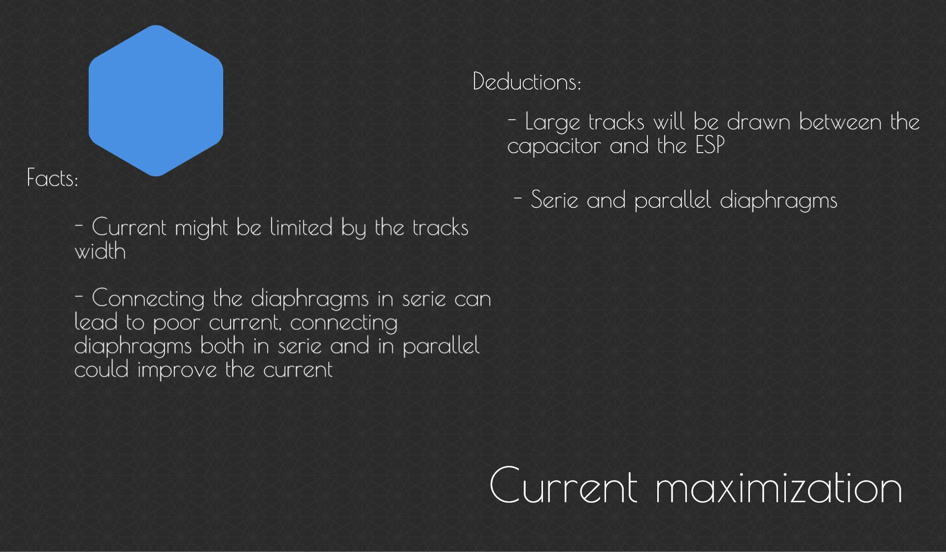
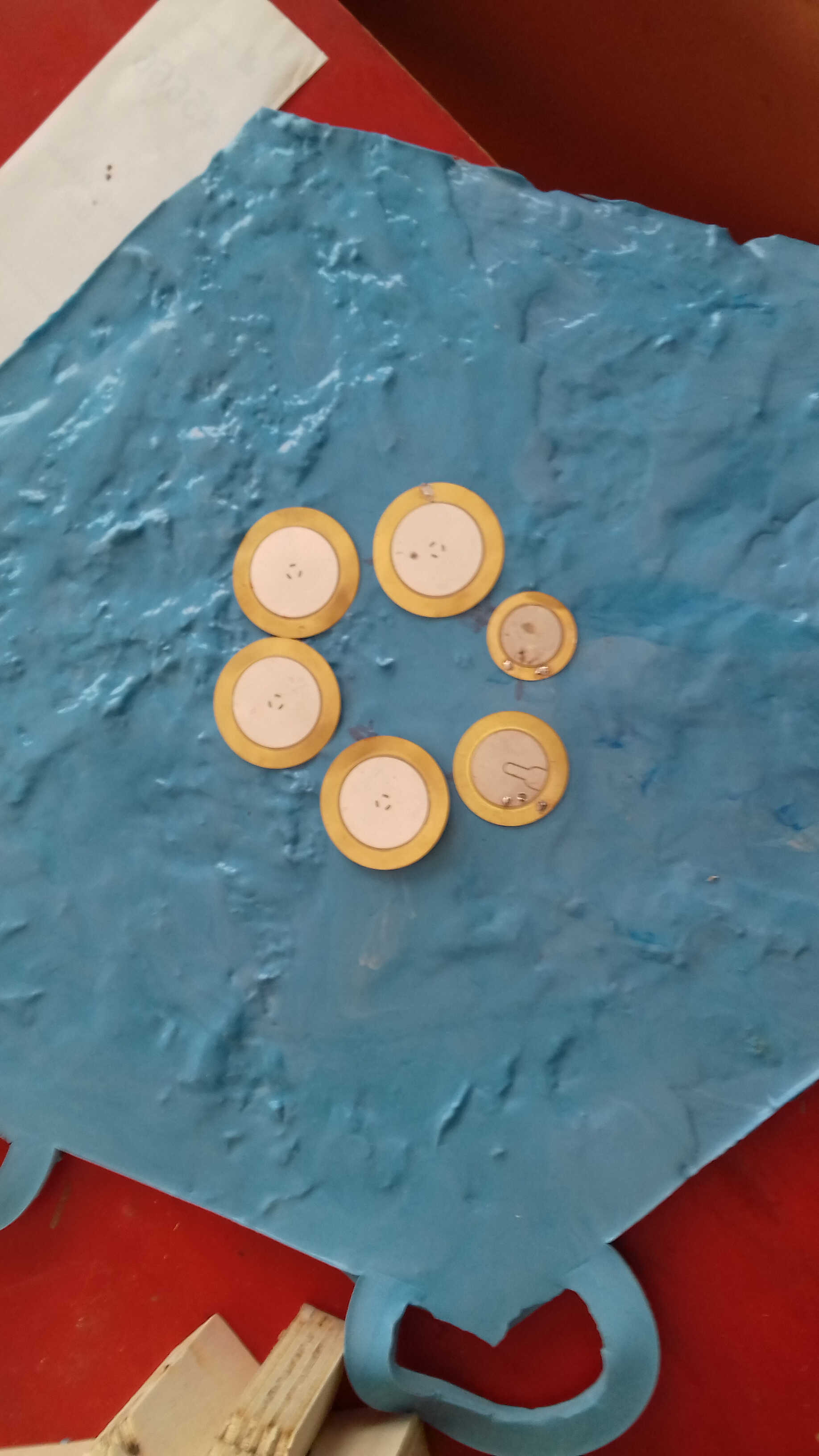
I ordered different types of piezo to compare their outputs (SMD, diaphragms, strips) and arranged them in arrays.
1 stripe could reach 1 V
2 stripes in parallel reached 4V and 0.5 mA
4 SMS piezo is parallel reached 3V and 2 mA
2 diaphragms reached 6 V and 2mA
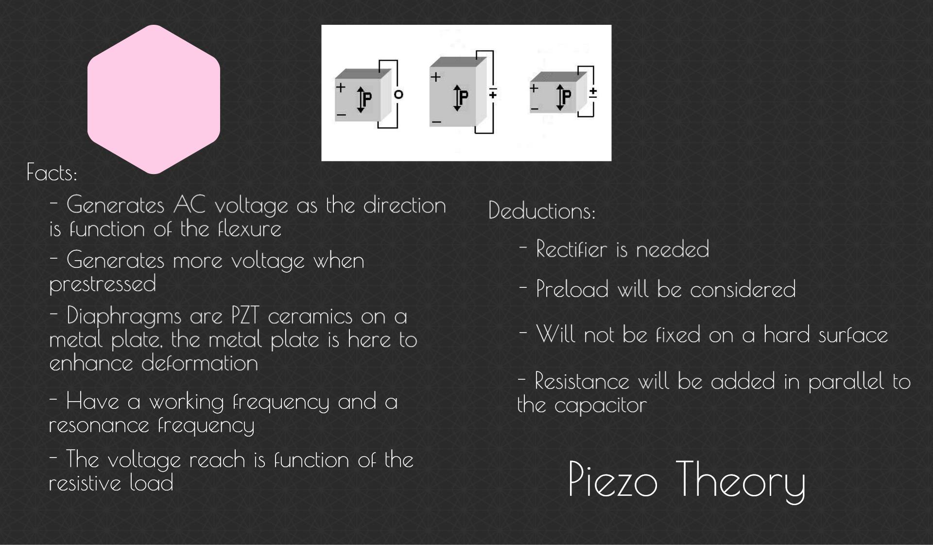
I noticed that the piezo released energy after the compression as if they were loaded. I read that only identical devices could be arranged in parallel otherwise they would charge and decharge one another. This may be what I observed.
2 stripes in serie reach 1.5 V and 0.3 mA
4 SMD in serie reached 1.2V and 0.1 mA
4 diaphragms in serie reached 15V and 2mA
4 diaphragms, 2 in serie 2 parallel, reached 20V and 3mA.
For those reasons I decided to go for the serie/ parallel mix of 6 diaphragms.
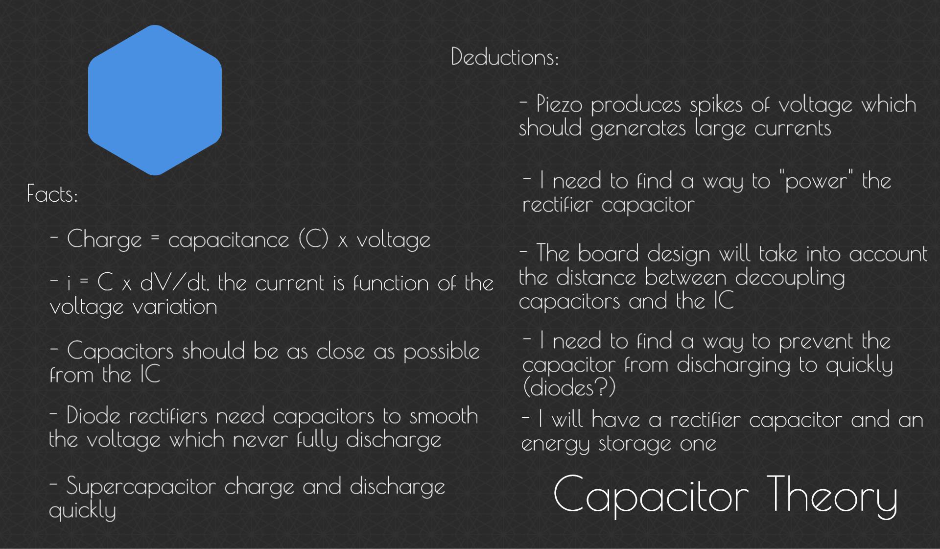
I also used the rectifier board I build for the group project to test capacitor value impacts. I tested capacitors of several order of magnitude but didn't observe big changes in the behaviour. For example I replaced the 1003 resitance by a 0 ohm one at the same time as I replaced a 1 microF by a 10 microFarad and the maximum voltage reached was 1.4V. I seemed to me that my board voltage was limited to 1.4V by the capacitor but I didn't know how to go further.
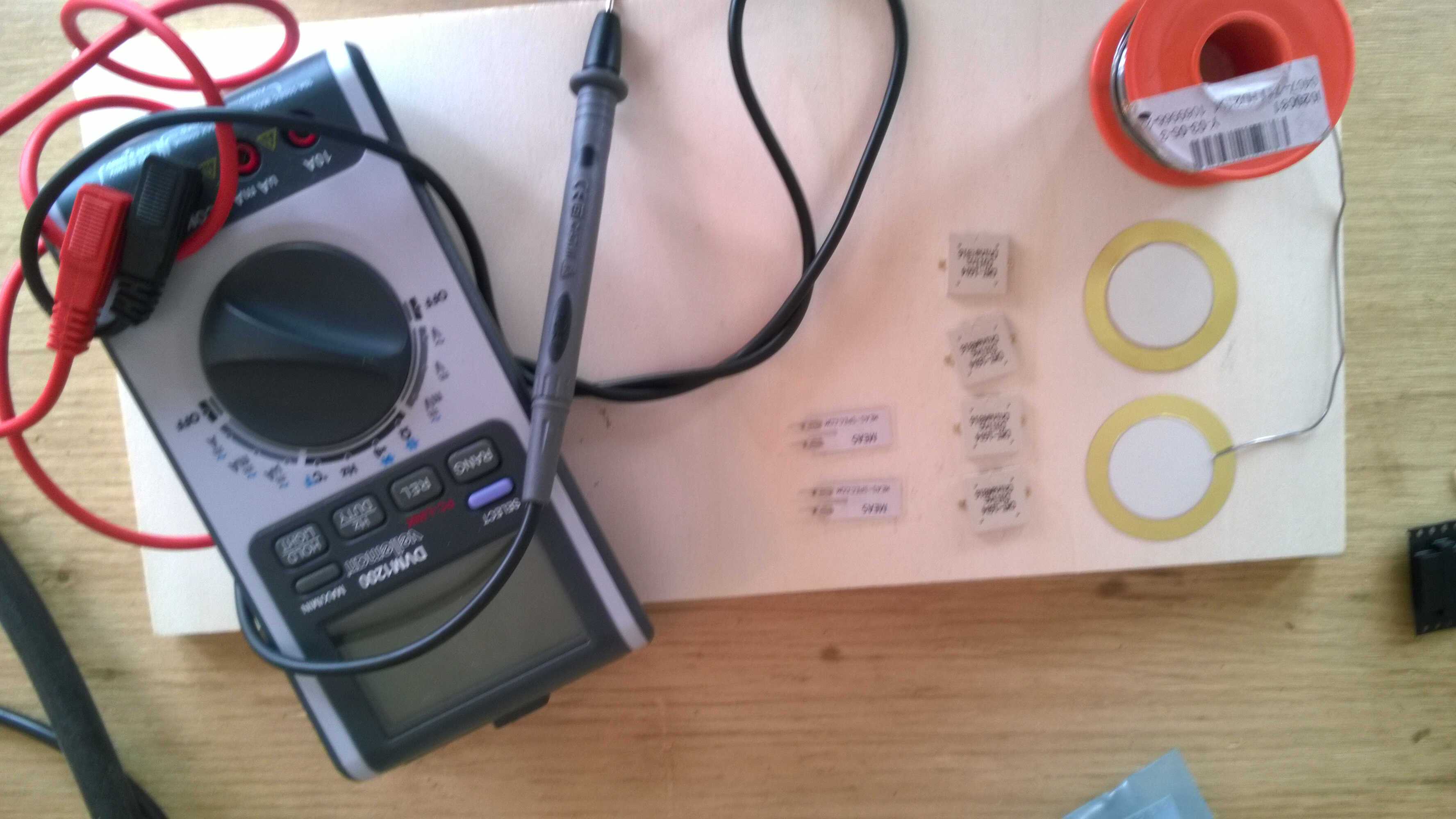
piezo variety
capacitor test
piezo + rectifier test
Design
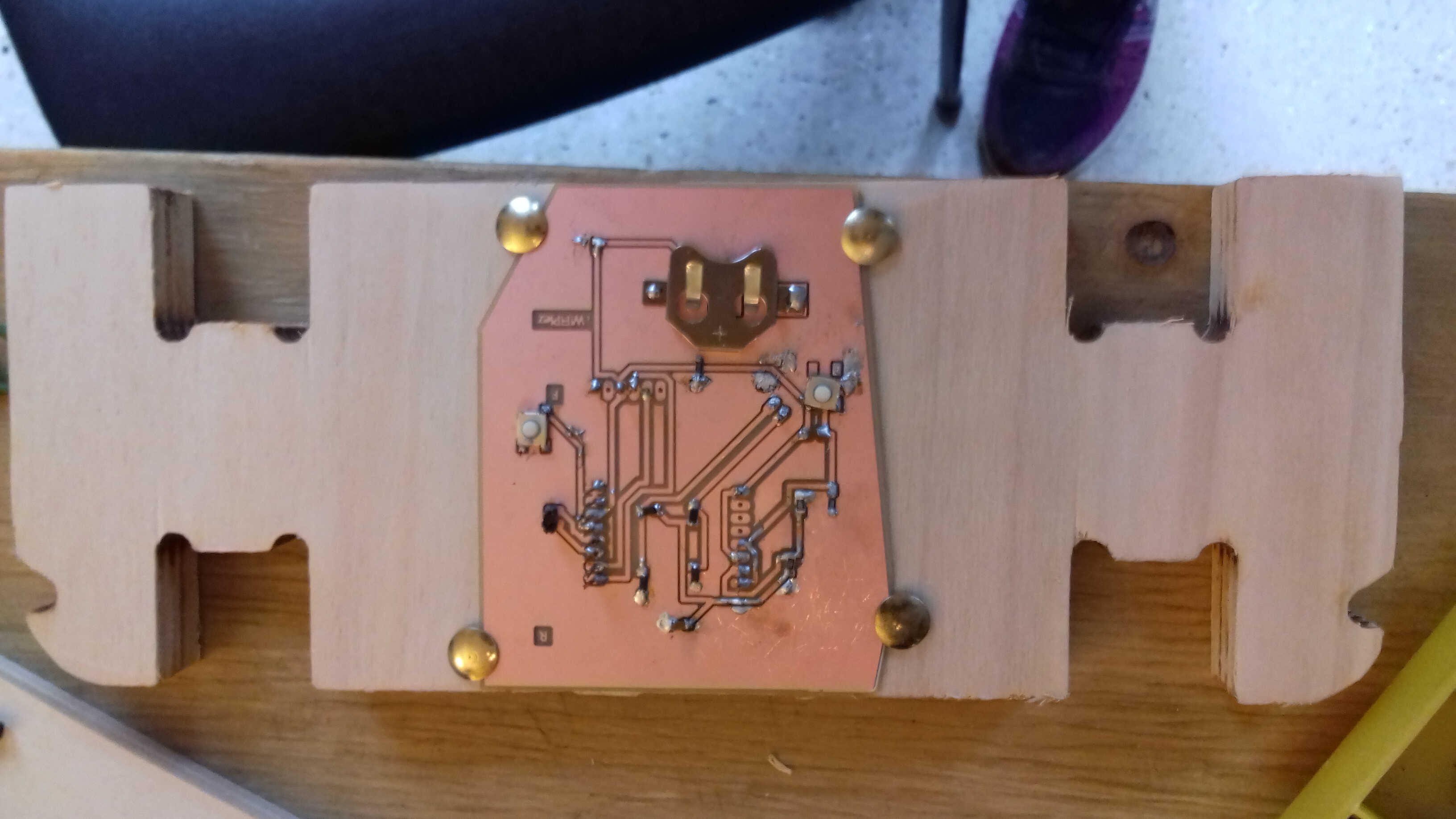
I designed the board with Eagle.
I tried to design 2 boards in parallel. One for the v1 of the project where the power produced is only measured. The second board being a board to power the ESP with the piezo, the power being smooth by a supercapacitor. As I had 2 board minimum to link to the ESP I decided to go for a ESP shield. Designing a shield wasn't as easy as planed I didn't find how to export groupes traces (the ones of the 3 connectors I wired to the ESP traces). I tried several export in vain, considered creating a new component based on those traces. Finally I went for a little hack. I just erased the ESP and reused the same schematic and board to which I added my new components.
For the board to look cleaner I tried to build a ground plane for the first time. I got most of it but ended with 2 separate grounds that I linked with a 0 ohm resistor.

board

ESP shield
Source file of the boards to load here
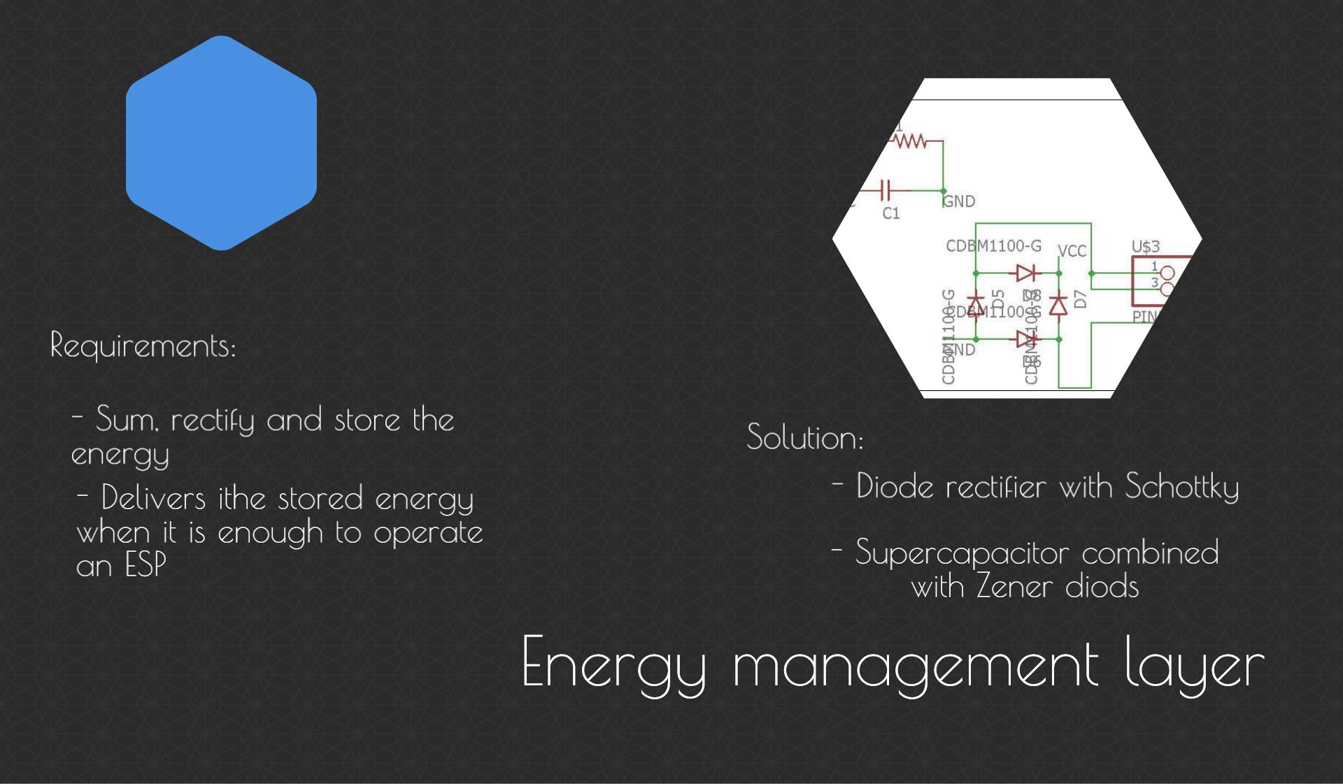
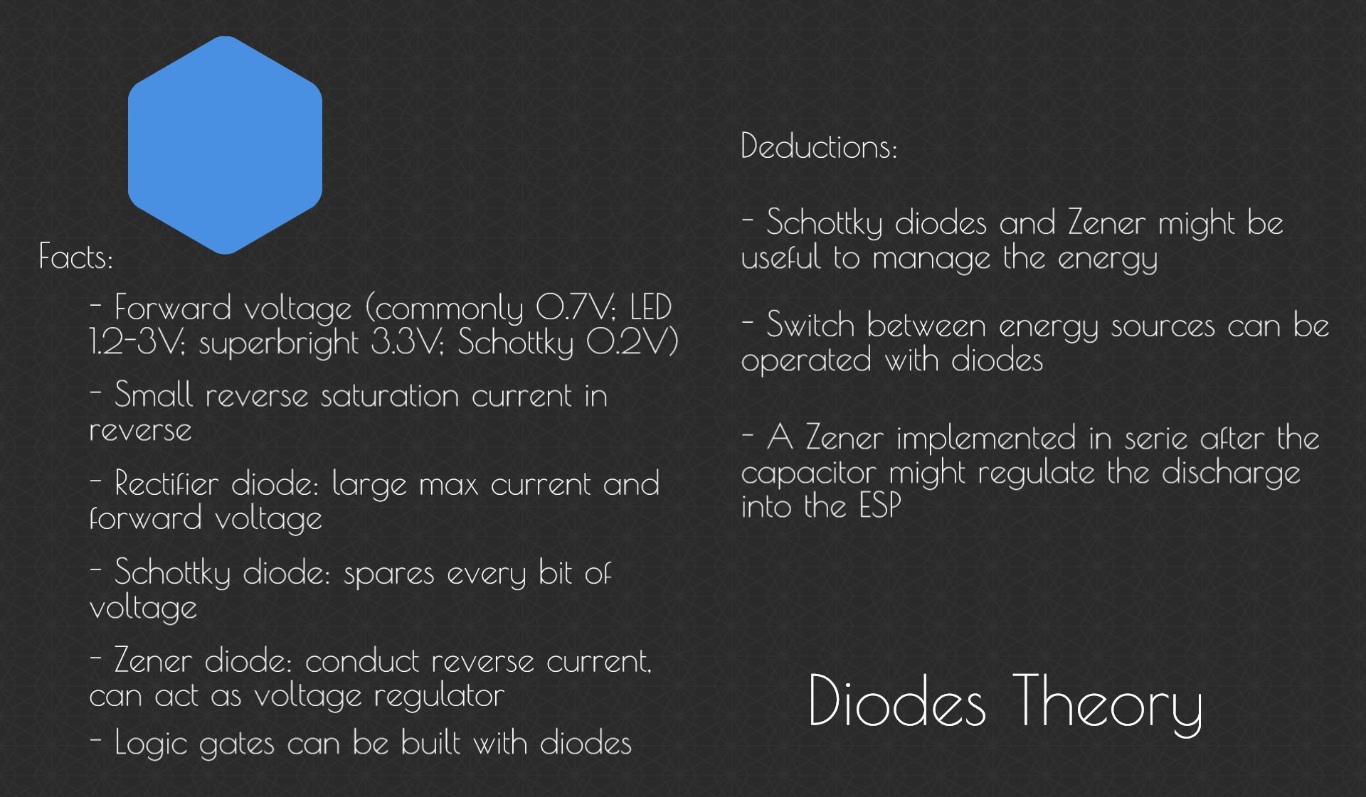
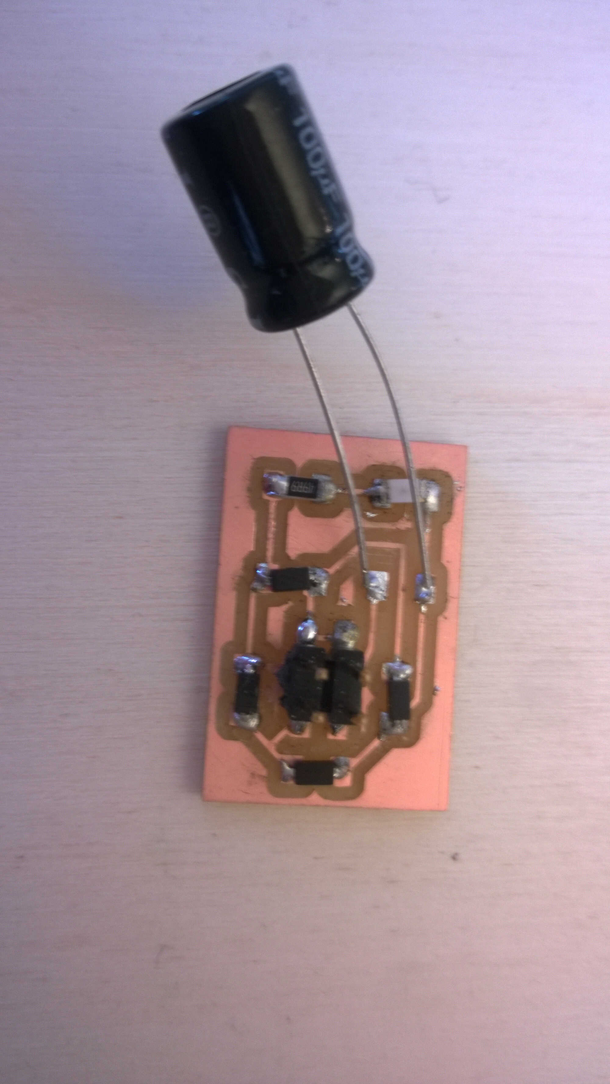
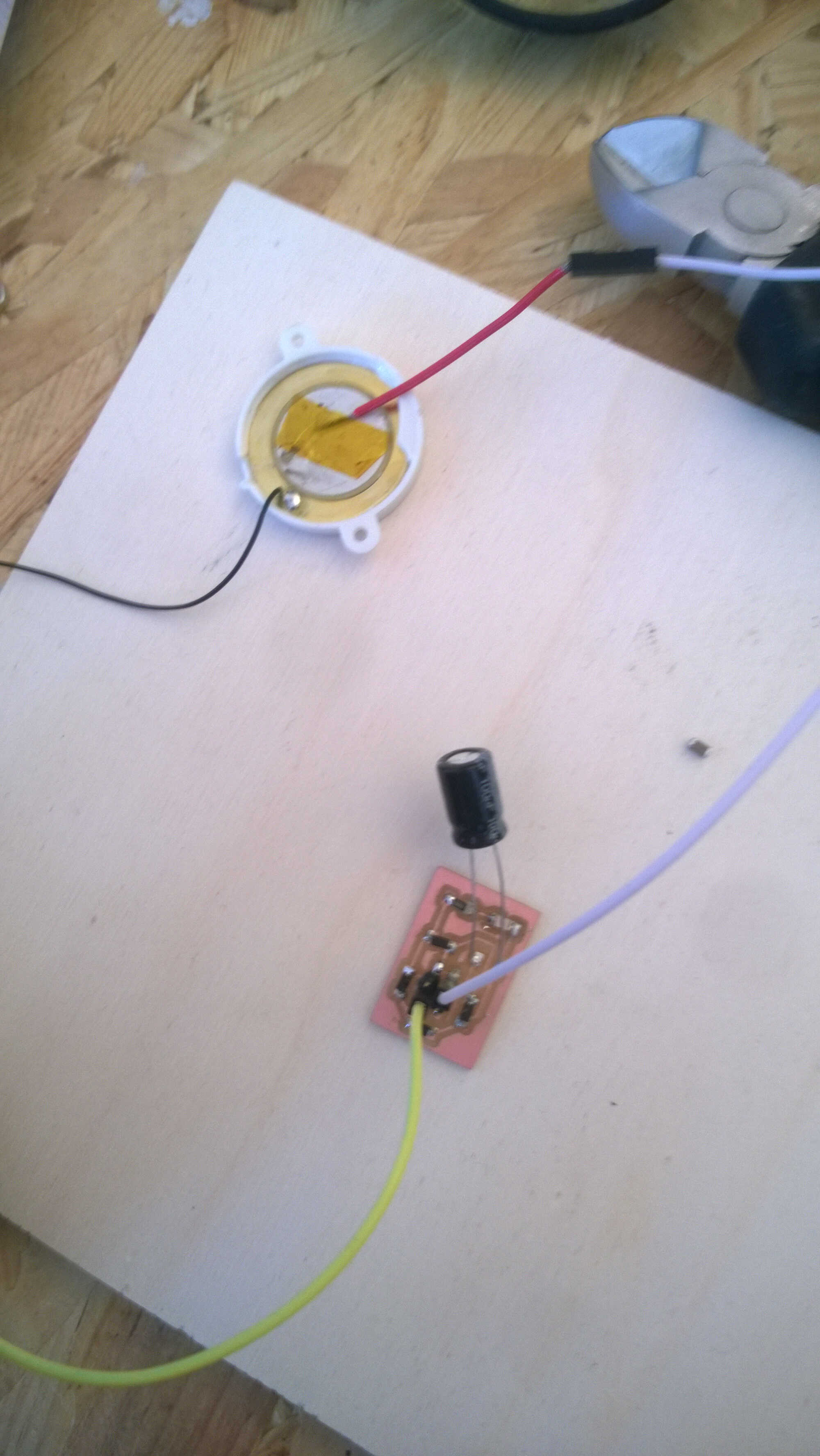
As piezo output alternative current it has to be rectified. Hence I designed a rectifier with 4 schottky diod and a 10 microFarads capacitor in parallel to smooth the output.
rectifier
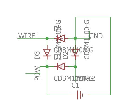
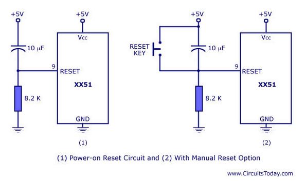
I wanted a reset button on my board but that requires some shematics because a simple button would produce a short circuit. I reused a schematic I found online with a capacitor (10 microFarads) and a resistance (1002/1000 Ohms). I also found this discussion quite interesting about reset pins.
online schematic
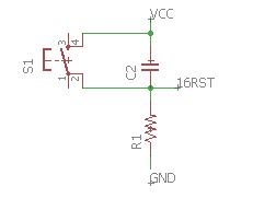
my schematic
I wanted a voltage at the ADC pin in the [0-1V] range. After the rectifiier the voltage reached 10V max. So I wnated a division factor of 10 for the divider. I tried with 1 and 10 Ohm, with 10 and 100 but my voltage dropped with those divider. I was given the advise by a friend to level up the resistors to higher values using the famous U = R.I formula. The amperage reached by the piezo is in mA/microampers for the tension to reach 10V the resistance (sum of the 2 ressitance bridge ) should be in the MOhm range (10/0.001=10 000 Ohm for mA; 10/0.000001= 10MOhms for microA). I chose the larger ratio ( MOhms and 1 MOhms) and my board had the behaviour I expected: volt range before the voltage divider, mV after and a capacitor that charge/discharge.
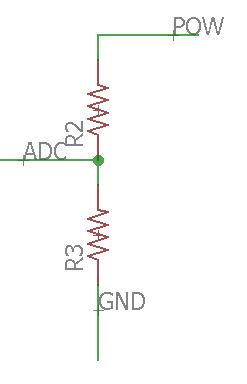
divider schematic
I wanted my board to be energetically autonomous, I had to change my project to more realistic measurement board. As my tile is supposed to be on the floor and outdoor it would make sense not to be wired. I looked at the ways to power 3V. My first try was with a CR2032 lithium coin battery but the amperage was quite low. Roman warned me. When I tried to power the board with it the voltage dropped to 0.6V. I found this piece of documentation on the comparison between CR2032 and AAA battery. So I fixed a coupler for 2 AAA battery using my cell batterie coupler as support with a zip. My module then worked smoothly.
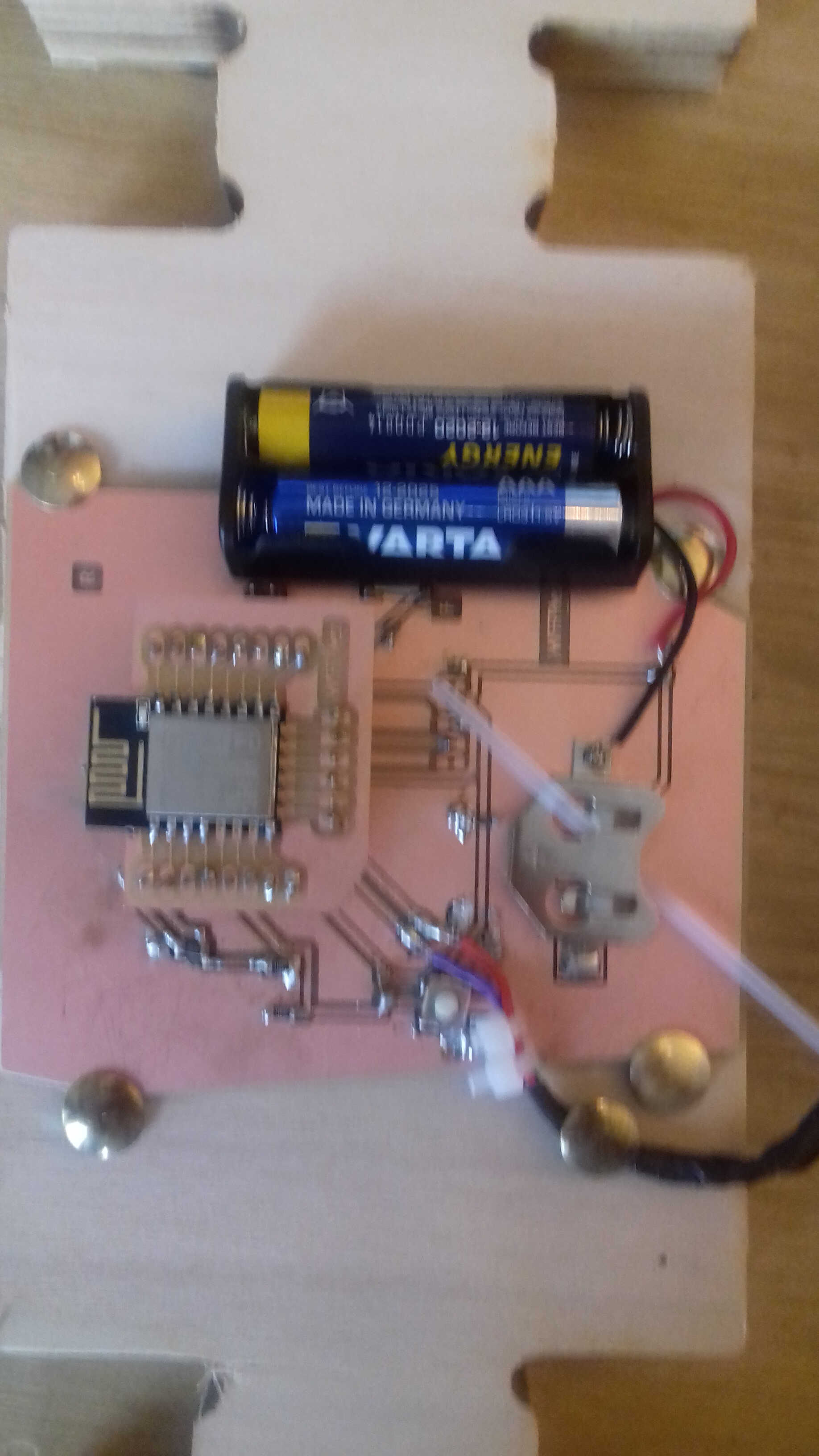
zipping couplers
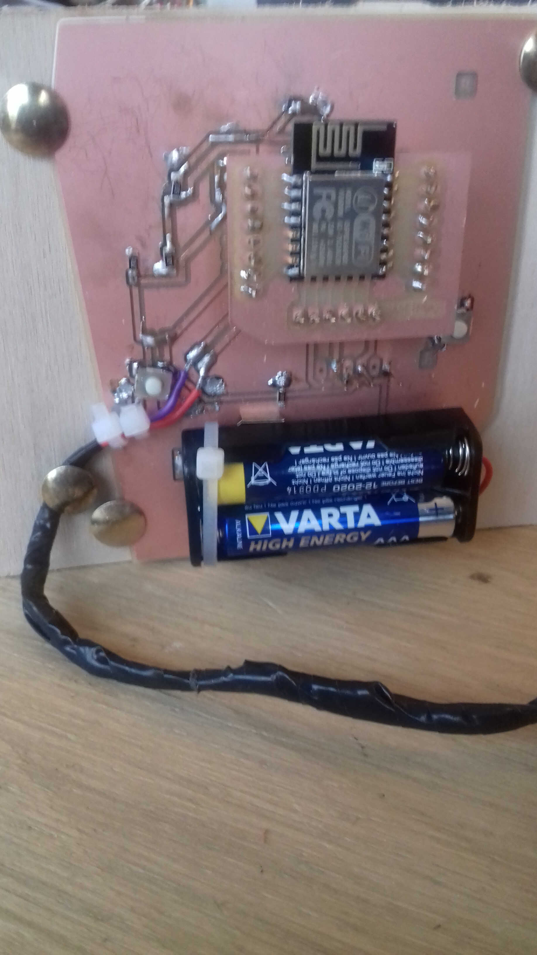
fixed couplers
As our CNC was down - a user tried to mill a tough material and broke the motor- I went to Digiscope to use their. Their CNC is slightly different, Romain showed me how to do the Z (by spinning and looking at the first copperr chips). This CNC is of greater precision and can spin to 15000 rpm. This is where I milled my ESP shield. I tried also to mill my measurement board but my traces were too thin (0.4mm). I then redesigned my board with 0.8 mm traces. This is where I found out about the ULP functionality. ULP is a script library. The script "cmd-change-br-width" allows you to select the traces you want to change the width. I also forgot some of the wiring required to flash the ESP (CH_PD, Reset, GPIO02, VCC to VCC and GPIO15, GND, GPIO0 to GND). By the time everything was fixed the motor arrived.
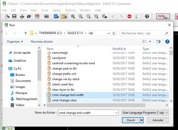
ULP library
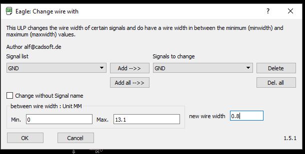
cmd-change-br-width interface
Piezo array
First I thought the piezo could be glued on the silicon. I pinpointed their placement on the silicon and made some tries with different glues (glue gun among others).None worked. All slipped away. I found silicon glue online but had no time to order one. I then had to find a hack. I soldered my array together and packaged them in tape.
silicon placement
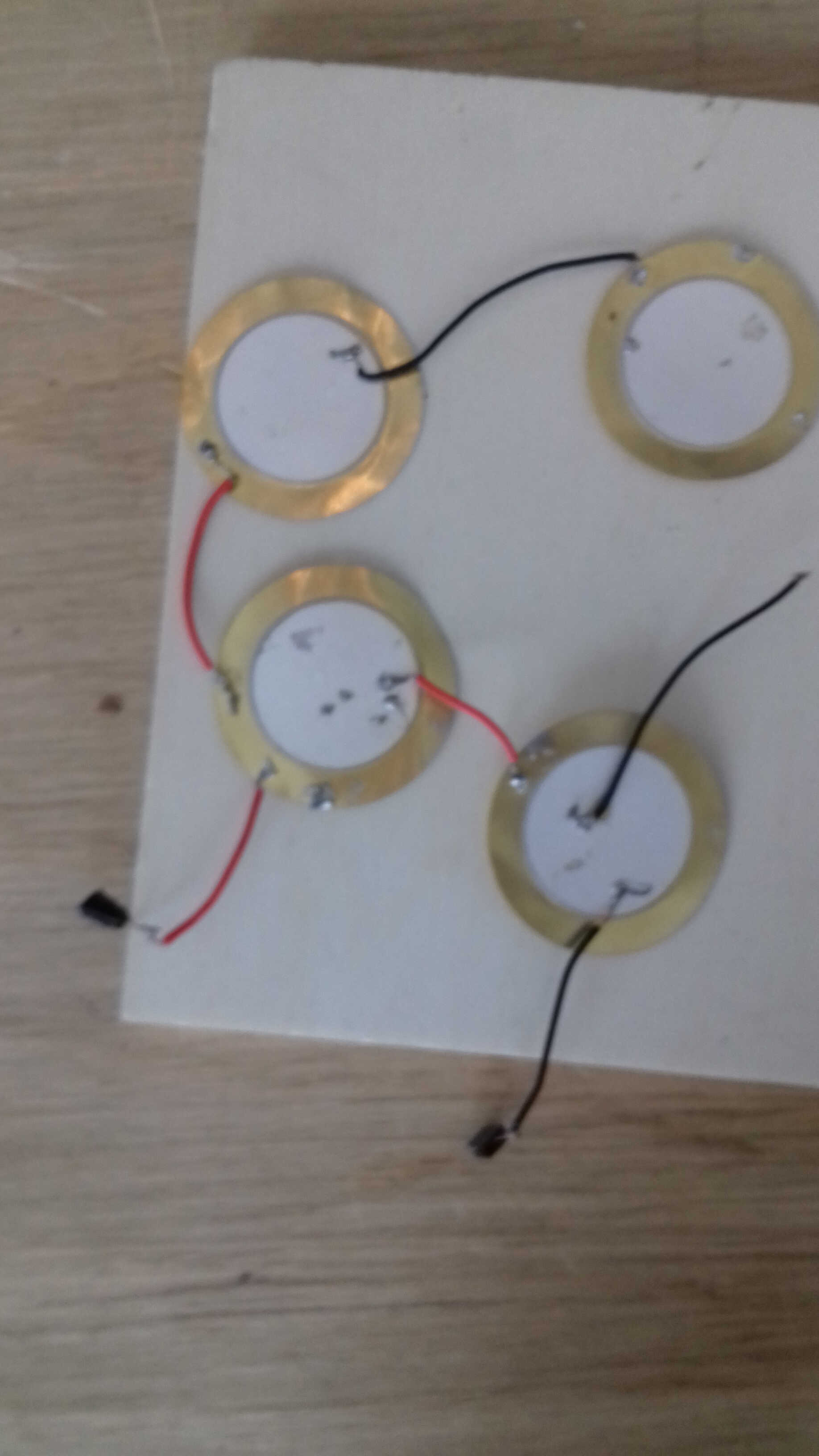
piezo array soldering
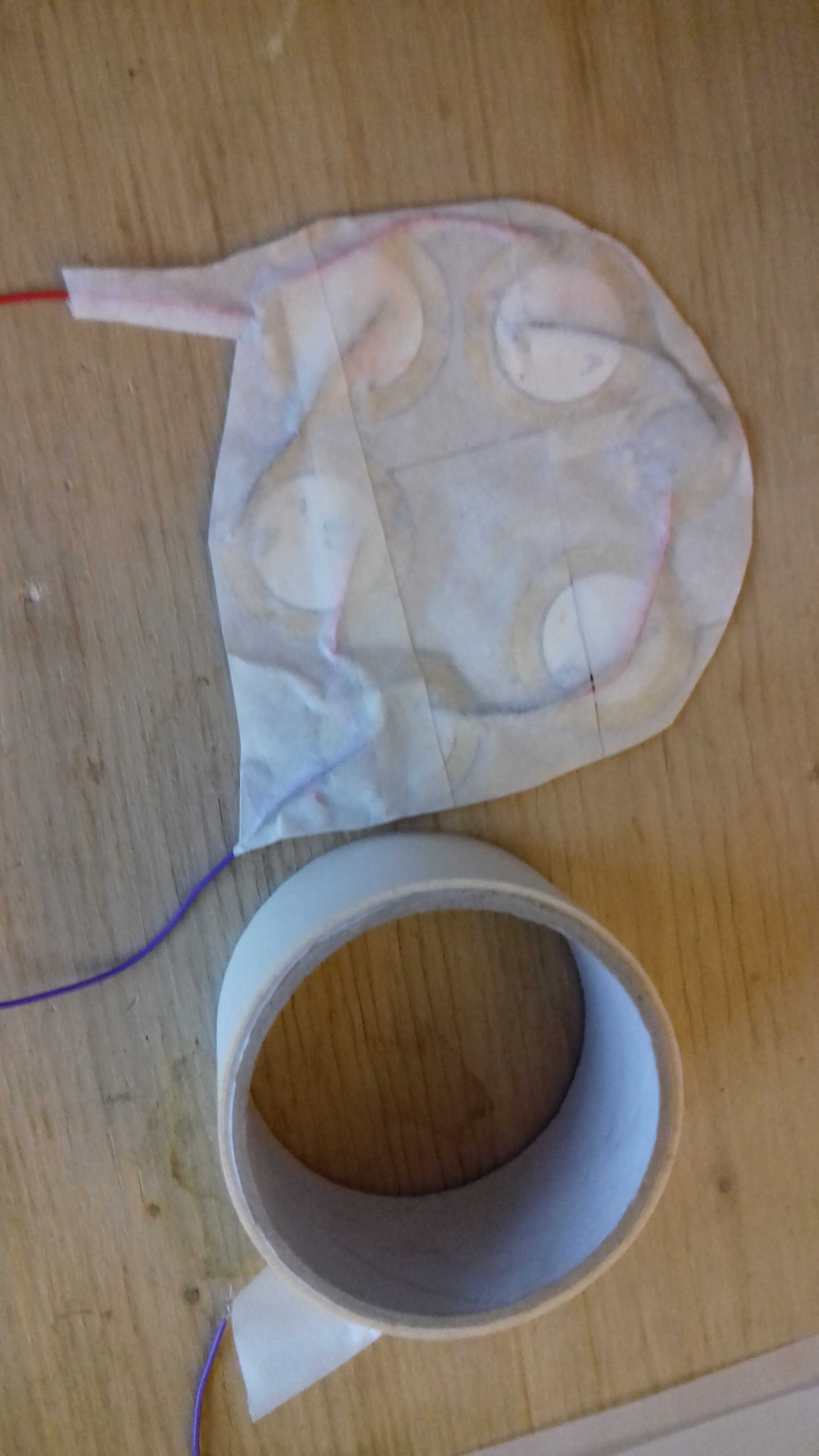
packaging piezo
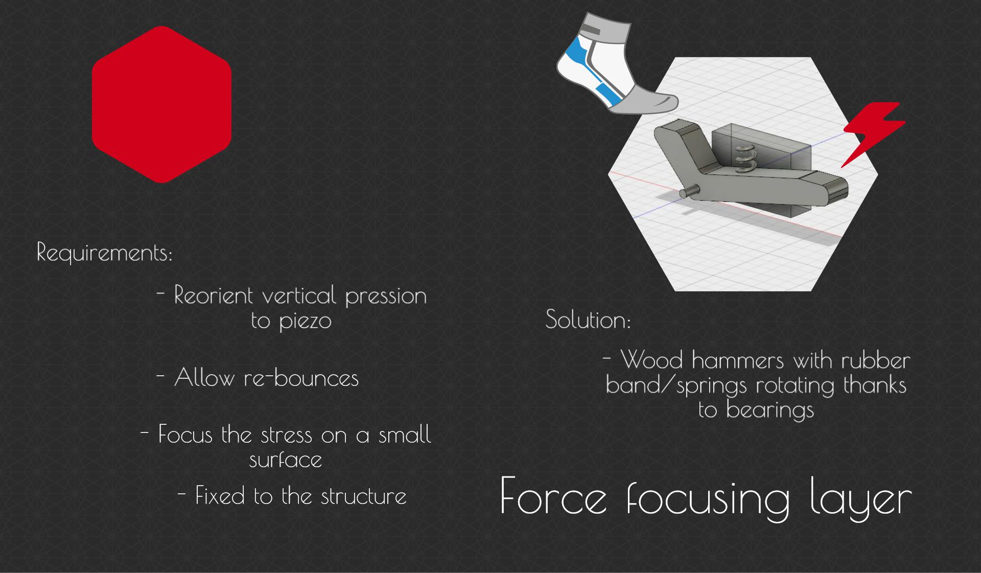
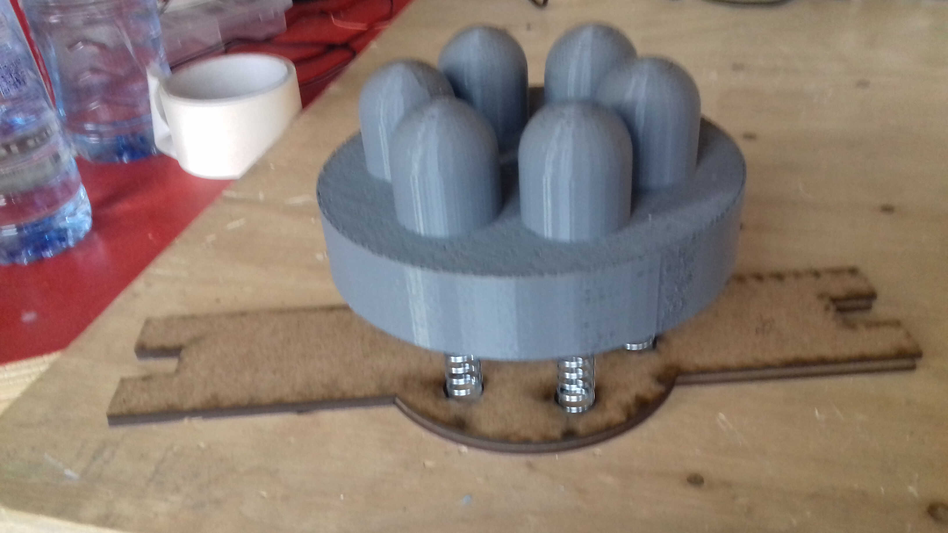
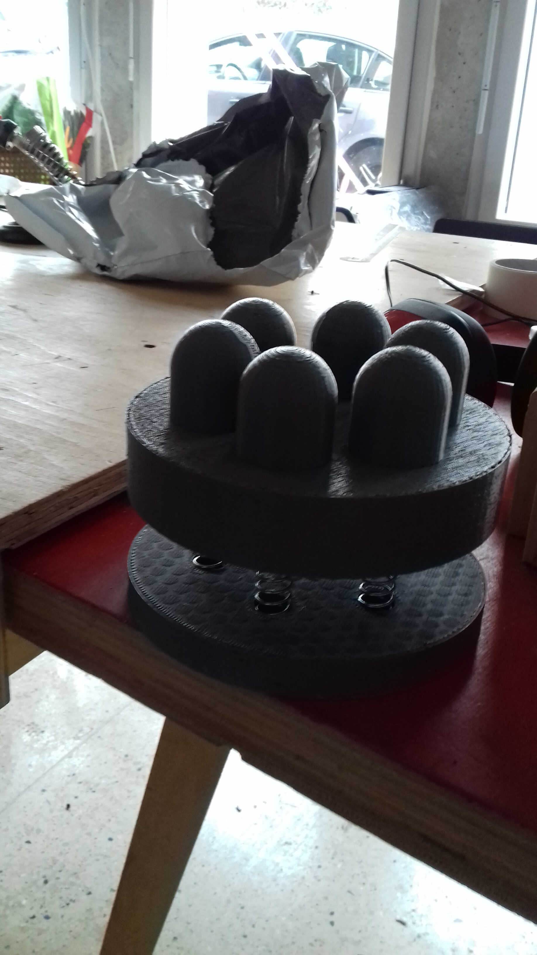
The mechanical part is supposed to maximize the piezo deformation. I read that pre-stressed piezo could deliver more. This why I wanted to add springs to the design. This would make the contact longer and repetitive. Also I wanted my sensor not to be invisible but to sense in the haptic way. I wanted also to focus the forces at the center of the piezo hence cone shapes. So this part is composed of 3 main pieces: a base and a top part printed in 3D as well as a lasercut medium piece to wedge the 2 first parts.
Design
The 3D pieces and the 2D piece were designed in Fusion and were based one on the other. The 3D pieces hosts 6 1.4mm diameter springs to provide elasticity. The 2D piece host the 3D base to keep the mecanism centered.
Source file of the boards to load here
Printing
The pieces were sliced in Slic3r and printed in grey PLA. As the top part would be subject to major stress I chose a 30% filling, which took quite a while. The bottom piece was printed with only 15% filling.
base being printed
Tests
The pieces react as I wanted and the springs stay in place.
top + spring
bounce
wedge
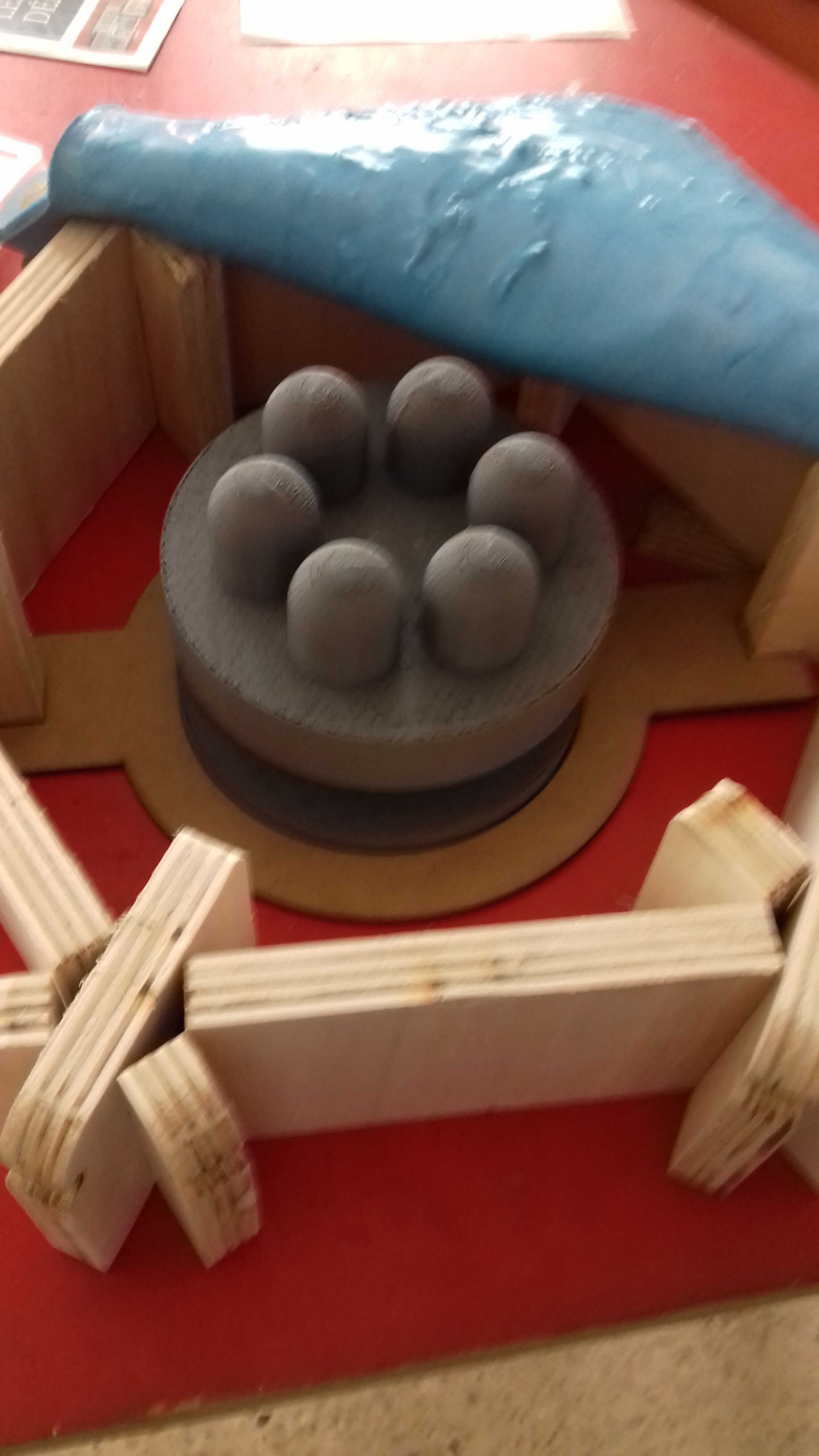
To integrate the different parts I mainly had to arrange the electonics. I fixed my board on the inside of my wood structure with pushpins. I joined the electrical wires with zip and electrical tape. The piezo array gathered with tape was fixed above the mecanical part with 3 rubber bands.
pushpin
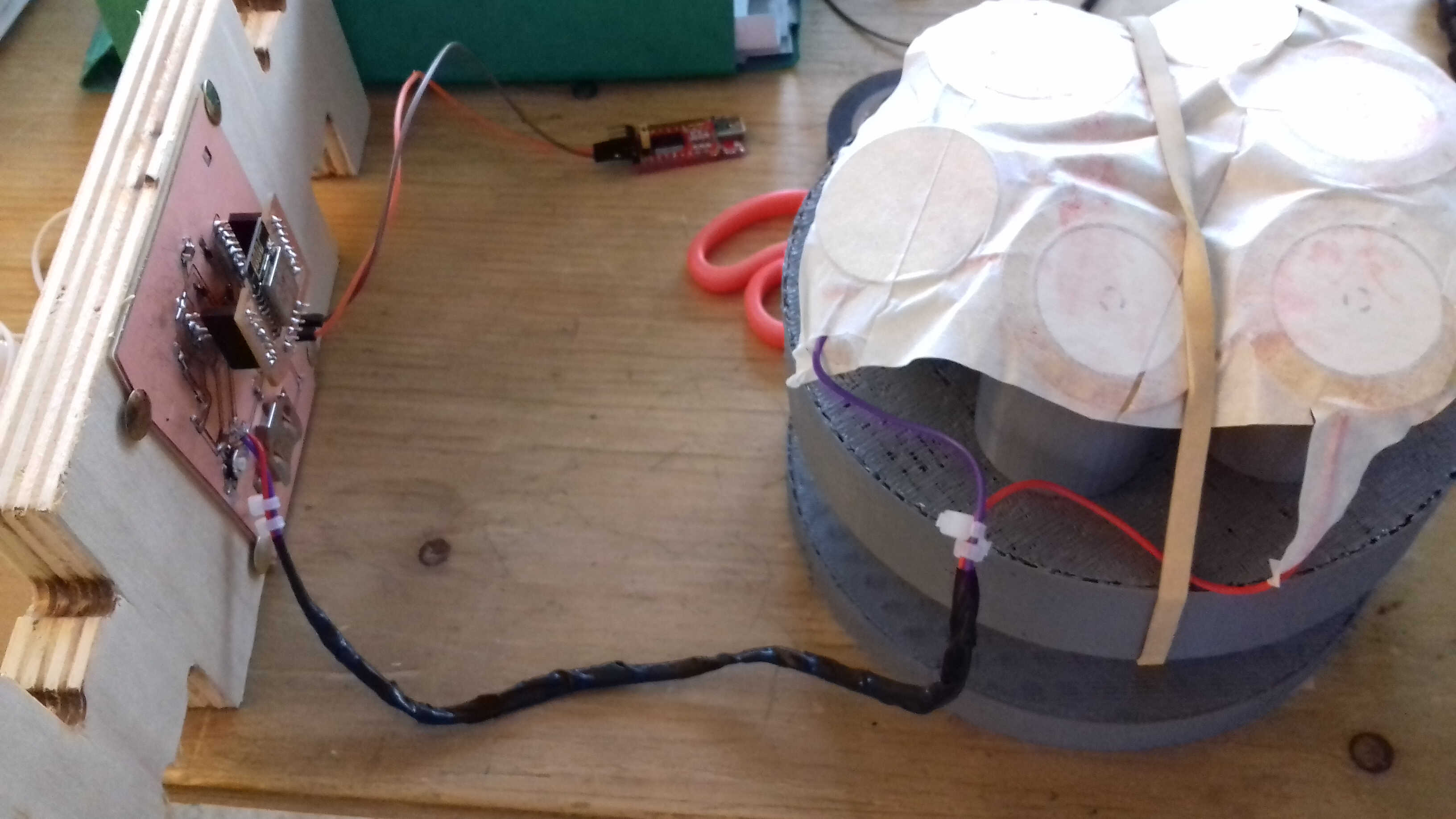
tape
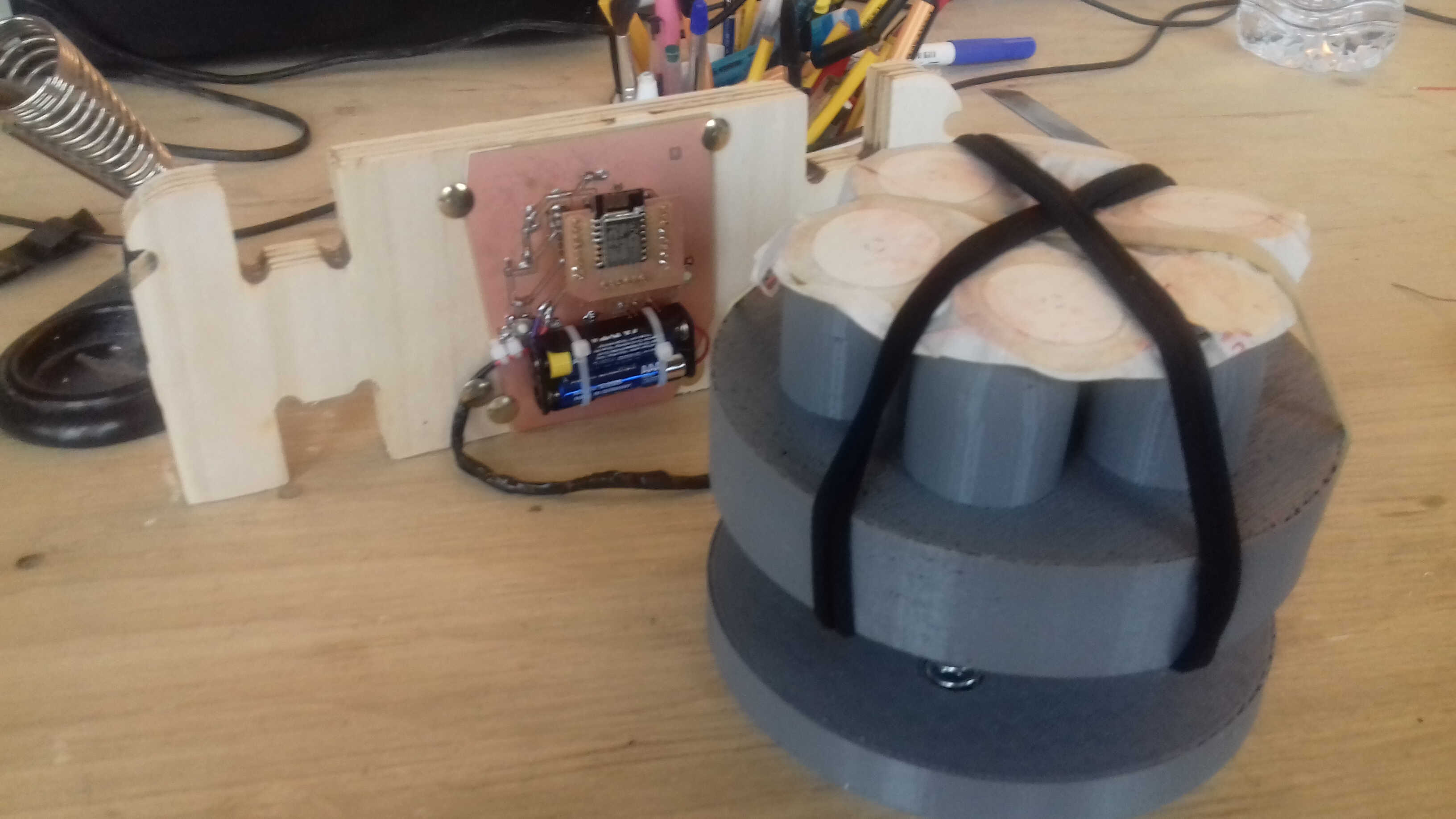
rubber bands
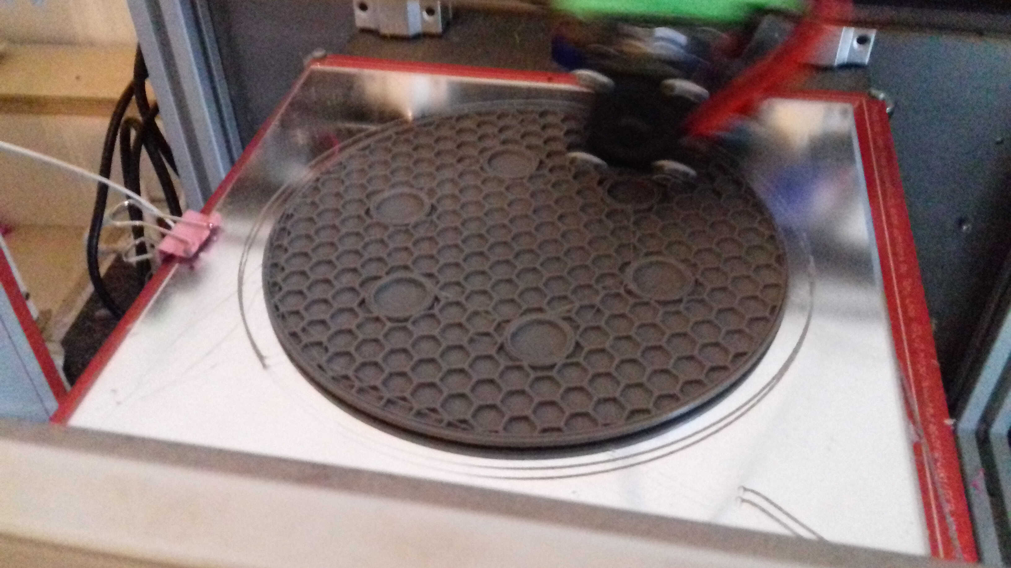
Then I put the mecanical part at the center of the structure thanks to my lasered piece. Covered the whole with the silicon. The module was set to go.
Video shown to Neil at an early stage.
Final demo:
Structure
- 1/4 plank poplar [20 euros]
- 30" CNC machine time
Covering
- 700ml silicon mix [20 euros]
- 3 medium planks 80x60 [20 euros]
- screws
- 30" laser cutter time
Electronical
- 1 PCB sheet
- 1 ESP8266 [3 euros]
- 4 Schottky diodes [1 euros]
- Connectors (6+8+8 female, 6+8+8 male, 2x2)
- 1 button [cents]
- 3 resistors (1MOhm, 10MOhms, 1 kOhm) [cents]
- 1 10microF capacitor[cents]
- 6 piezo diaphragms [10 euros]
- Wires
- Tape
- 1 hour CNC machine
- 2 hour soldering
Interface
- Register on Blynk
- 30" flashing/programming
Mechanical
- PLA 1/8 of a reel [10 euros]
- 10 hours of 3D printer time
- 1/4 of a medium plank (80x60) [2 euros]
- 15" laser cutter
- 6 compression springs (1.4 cm diameter) [10 euros]
Integration
- Rubber band
- Pushpin
Total
One module comes to the price of a hundred euros. I suppose scaling would reduce the cost. If I add the tests costs I am around 120 euros, which is quite expensive.
As detailled in Week 18 I chose a Creative Common licence so that my prototype can be improved. I am well aware that my final project is now just a prototype. An electronical engineer could probably easily improve its effiency for example. I suggested some improvements in the Future development section.

licence
Structure
By trying and testing I noted that this concept could be modified to become a seat. For example one that can be found in the subway. For this to work the structure would need to be modified into something slimmer and rounder.
Covering
As mentionned earlier the coves should be made rounder so that the stress doesn't get focused at the angles. I experienced some tearings, maybe those parts should also be thicker (+3 mm). Also another type of fixing than coves could be tested such as clamping.
Electronical
Amperage
As mentionned earlier the purpose of this board is to be self-powered. To do so the amperage should be improved. It would be possible at first to measure the amperage the same way I did with voltage. This could be done with a tore and hall effect sensors as demonstrated here.
For the amperage to be raised several options should be explored:
- a bigger piezo array
- a current amplifier A current amplifier can be bought (example ultra low current amplifier) or made with transistor following those type of scheme (instruction link):
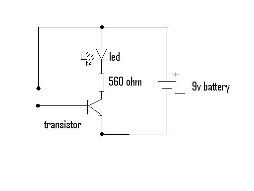
led amplifier
double transistor amplifier
- the combination with an other source of power: an electromagnetic one for example(discussed here and there). As we have a moving part the movement could be used to displace magnets in coil. I tried to build one with a solenoid plunger and a copper wire, with no success. I suppose I didn't have the good kind of magnet.
Storage
As for storage I designed a first board. It had a supercapacitor at the place of the regular one and a Zener diode at its exit to regulate the current which would power the ESP. I think this combo is the right one as I found it in other applications.
Mechanical
The mechanical parts could be modified to host a MEM generator or activate other kind of piezo for example SMD between the base and the top parts.
Integration
It could be made prettier especially the fixing of piezo on top of the mechanical part. The piezo array could be sawn on a strechable material which could be fixed at the hooks. This is very TextileAcademy.