Week6 : Electronics Design
The assignment of this week :
Redraw the echo hello-world board, add (at least) a button and LED (with current-limiting resistor), check the design rules, and make it.
● Redraw the echo hello-world board
Although I had experience of making PCB before, but I I were not familiar with the milling mechine and software the lab used. At first I readed the tutorial, and follow the step to redrawed the circuit with Eagle. On this step, I found it was a little perplex to find the corresponding package of the component. Although I download the libraries which was provided from the tutorial, it still spent some time to found the component. I spent a little time to get familiar with the software. Then I found Eagle was an convenient software of designing PCB. When I went to make a PCB, there were two steps needed to do.
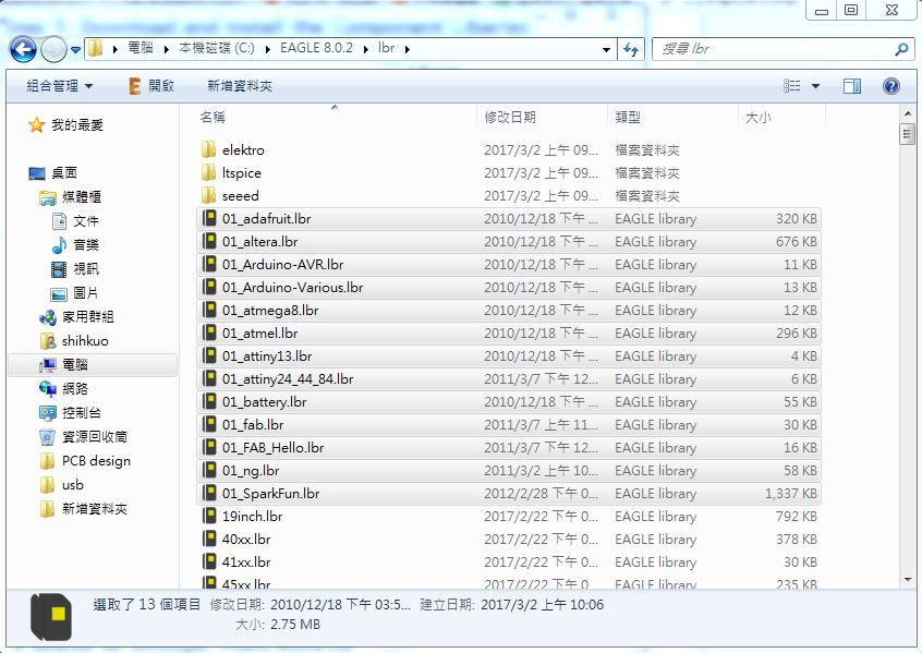
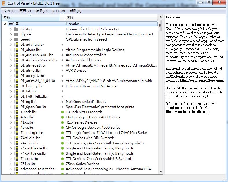
figure 1 : Download and import the libraries.
First, I needed to draw a schematic, and I added a led and button on it. It was necessary to give each component's footprint an net name, and these nets would help me to connect the corresponding pins during the follow PCB layouting.
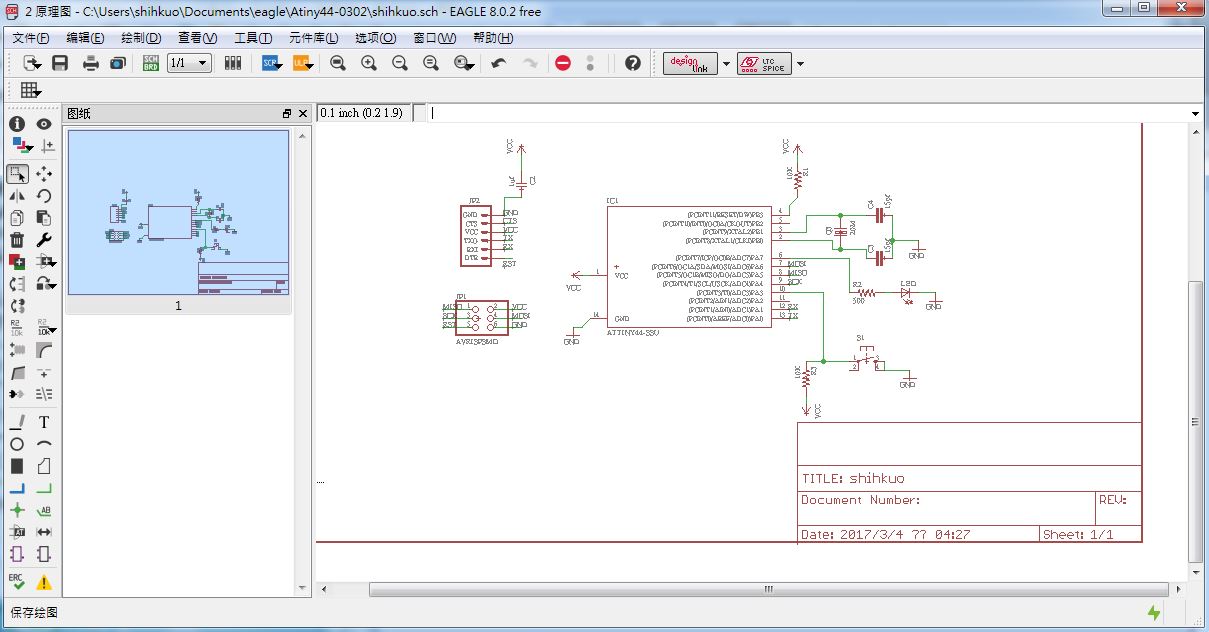
figure 2 : Draw a schematic.
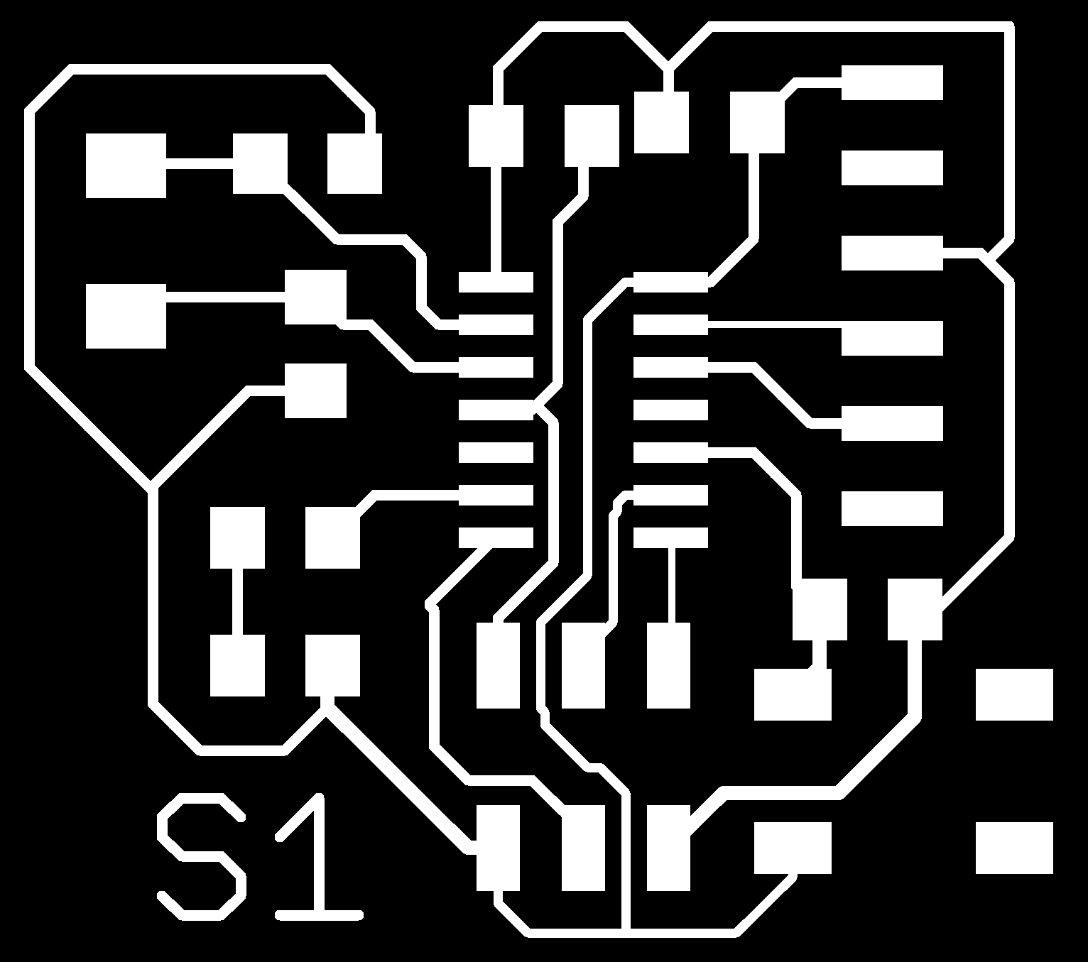
Second, I needed to layout the board. While finished the schematic, I just only pressed the button which was "Go to the top menu > File > switch to board" and it would switch to the board view. I only placed all components on the proper place, the used the autoroute funcation which was "Go to the top menu > tool > autorouter " and Eagle would finish the routting for me.
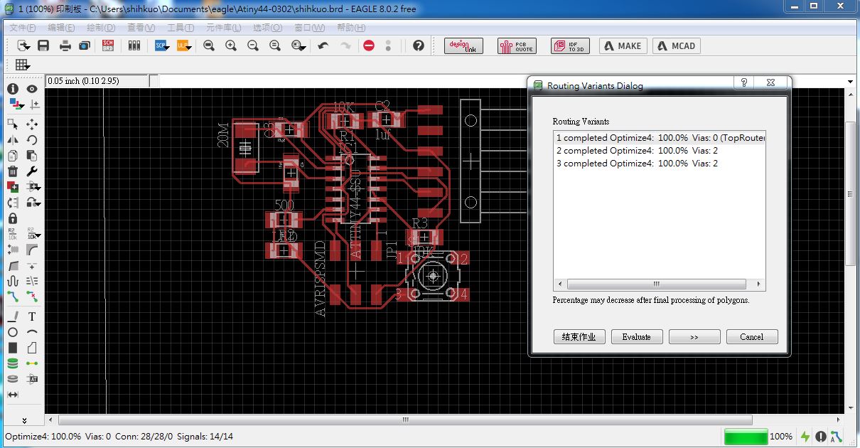
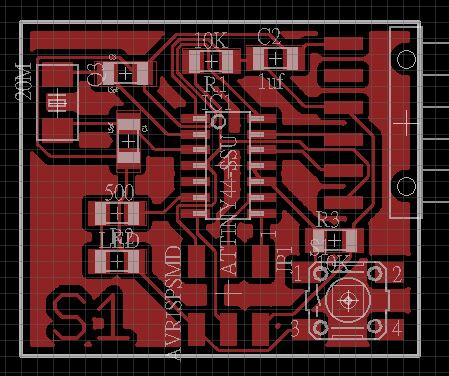
figure 3 : Use "autorouter" funcation to finish the PCB layout.
● Milling the echo hello-world board
Also, I used Roland Modela MDX-20 to do the milling. I converted the PCB to the png format and improt it to the fab module. After milling the first PCB, it looked terrible. Some traces were milling out, and some pads and traces were sticked. I thought the problem might be the resolution setting while converted to the png format. Then I increased the resolution and tried again. The second PCB looked better than the first one, But it still had some pads and traces sticked together. I realized that might be the problem of autorouter, same traces and pads were too closed to milling them separated. So I dicided to giveup to use "autorouter" to do the layout. I layouted the PCB again by myself and iccreaseed the space between traces and pads. After milling serial times, the PCB looked good.
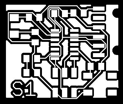
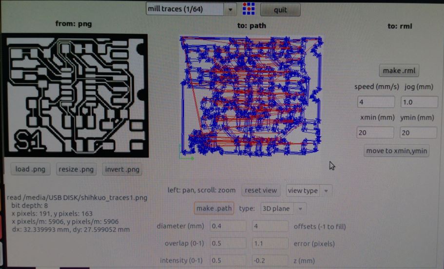
figure 4 : Convert to png format anf import to fab module.
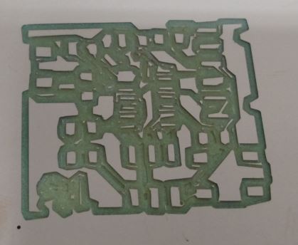
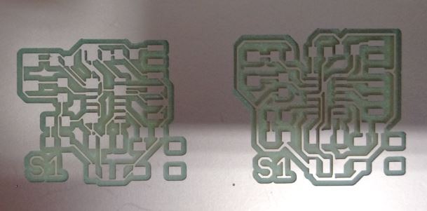
figure 5 : Some traces were milling out and increased the resolution then milling second time.

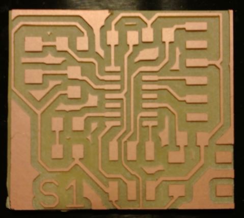
figure 6 : Routed again manually and milling looked good.
● Soldering the components
I had practiced soldering components two weeks ago, so it was not difficult to me. After soldering all components, I used the digital multi meter to check the connection of each pin. All I had confidence of my PCB, I still found a short circuit. I looked close to check the traces, pads and solders, I finally found that there was a trace and a pad slightly sticked. I used knife to cut them out and checked again, the short circuit check passed.
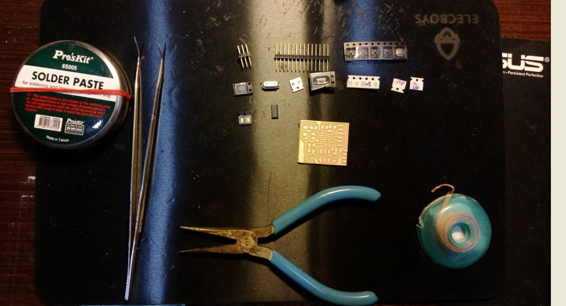
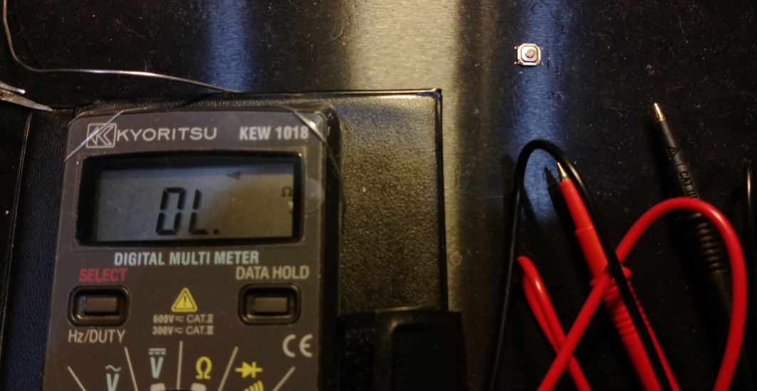
figure 7 : Soldering the components and check button's short circuit side with digital multi meter.
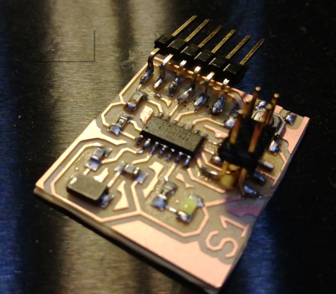
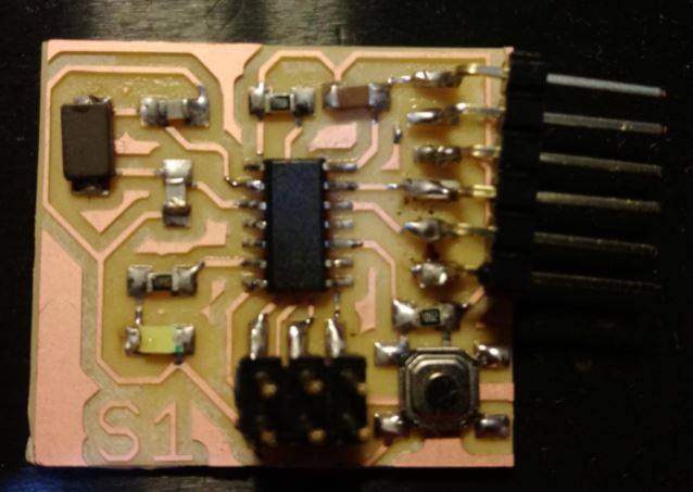
figure 8 : Finish the PCB.
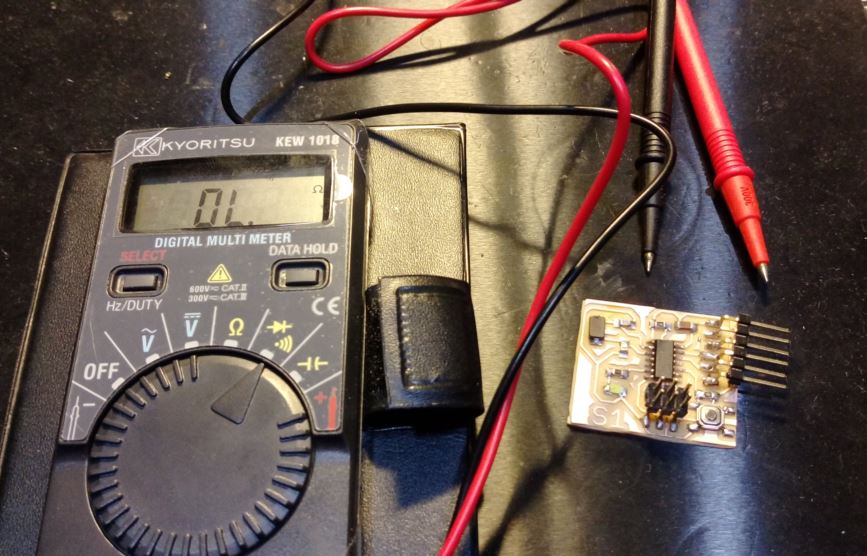
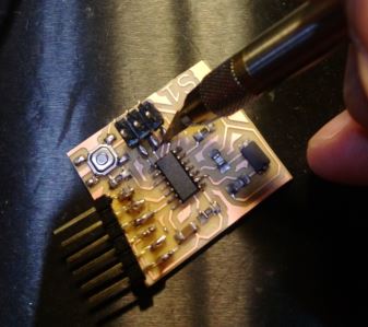
figure 9 : Use the digital multi meter to check the connection of each pin, and cut out the short circuit part.
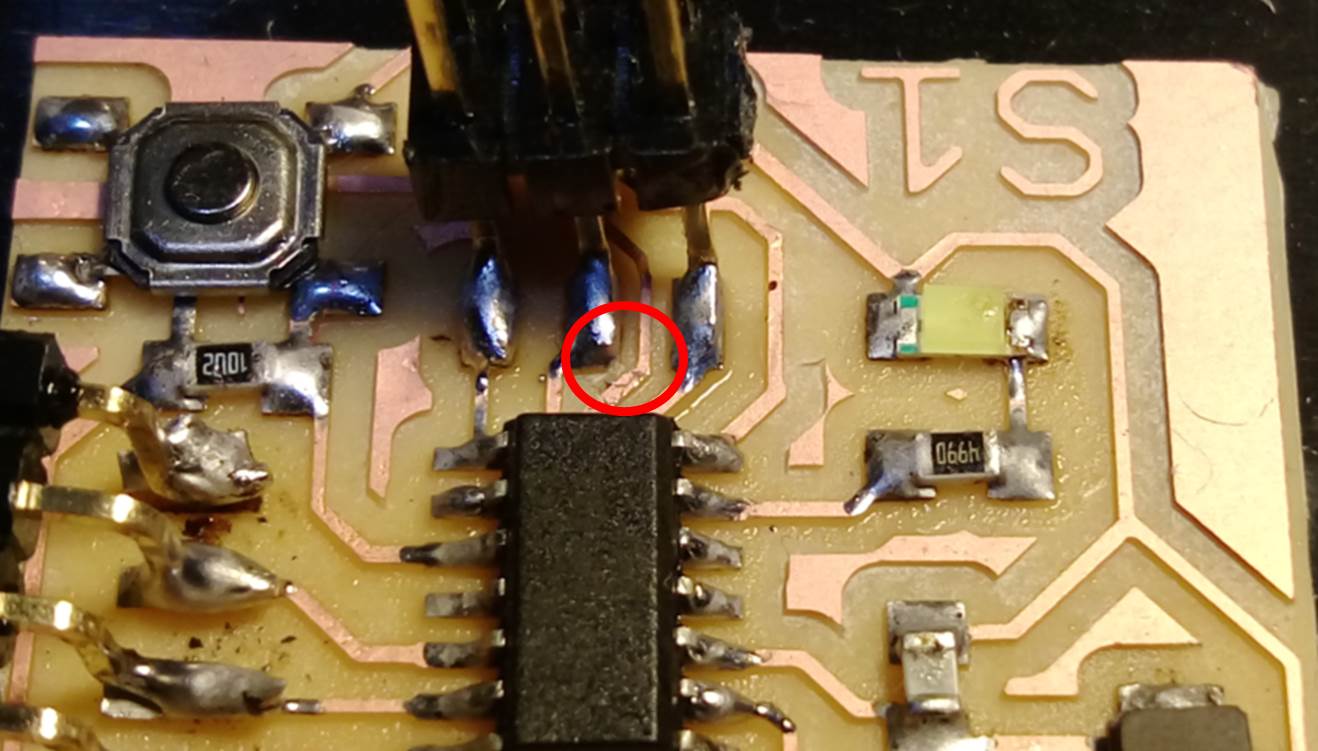
figure 10 : Short circuit part checked again and passed.
● Source file
1.Attiny44 datasheet
2.eagle_libraries.
3.Schematic of the PCB.
4.Board layout of the PCB.
5.PNG format of the traces.
6.PNG format of the interior.