Week4 : Electronics Production
This week has two assignments:
1.Describe the process of milling, stuffing, de-bugging and programming.
2.Demonstrate correct workflows and identify areas for improvement if required.
● Milling the PCB
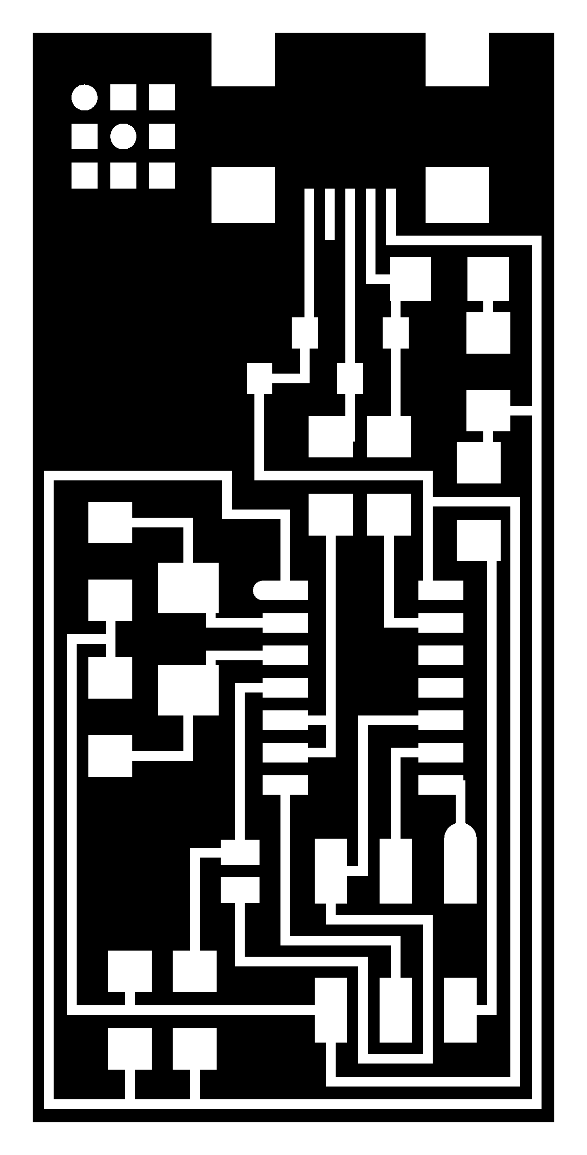
In our lab, the mechine we used to mill the PCB is Roland Modela MDX-20. First, I decided to make the version of FabISP is "hello.ISP.44.cad", so I downloaded the layout (traces) and the interior from the lectures website.
Second, I fired up the terminal in Ubunto and started the fab module. I should selectd the format I want in the first dialog box. For making the PCB with modela, the setting liked bolew:
From format: image (.png)
To format: Roland modela (.rml)
The setting of milling the traces was below:
Type:3D plane
diameter(mm):0.4; Offsets:4
Overlap:0.5; error(pixels):1.1
intensity:0.5; z(mm):-0.1
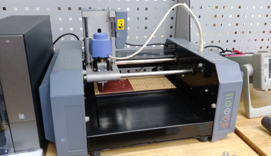
figure 1: Roland Modela MDX-20.
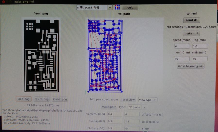
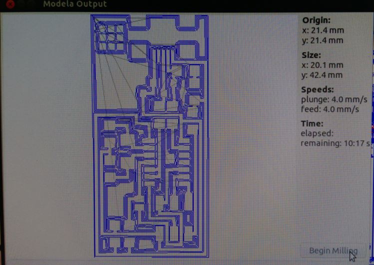
figure 2: The setting of milling the traces.
Before milling, I should zeroize of z-axis manually. This step would affect the setting of parameter "z(mm)".
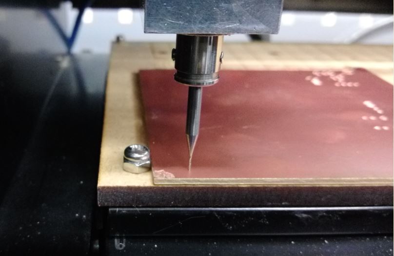
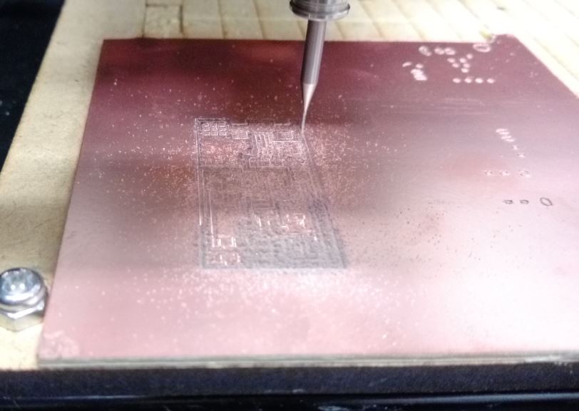
figure 3: Zeroize the z-axiz and Milling the traces.
After finishing the first milling, the traces were not cutted clearly. So I changed the value of "z(mm)" from -0.1 to -0.2, and milling the second board. The result of the second board is that it could milling all the traces, but the depths were different. The depths in the front of the board were deeper than the back. I realized that the base board of the mechine might not be in the same flat. Then I changed the base board and millinged the third board. The result of the third board looked well than others.
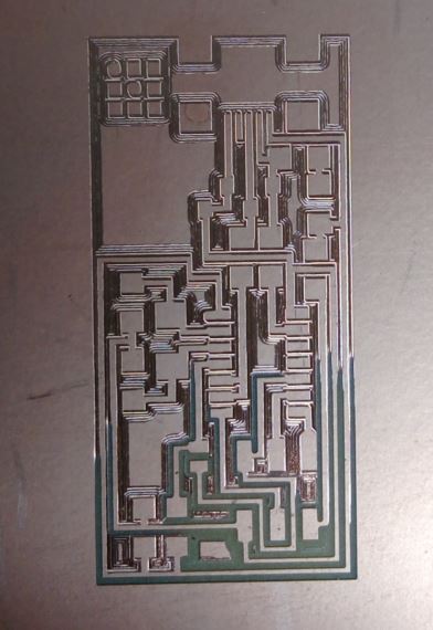
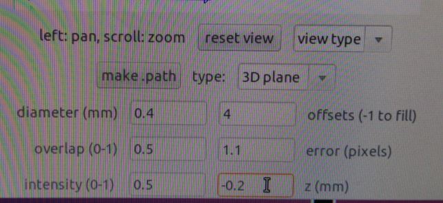
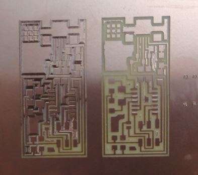
figure 4: The comparison of depths between two board which changed the setting of "z(mm)" from -0.1mm to -0.2mm.
The setting of milling the board was below:
Type:3D rough
diameter(mm):0.79; Offsets:1
Overlap:0.5; error(pixels):1.1
top intensity:0.5; top z(mm):-0.6
bot intensity:0.5; bot z(mm):-1.7
cut depth(mm):0.6
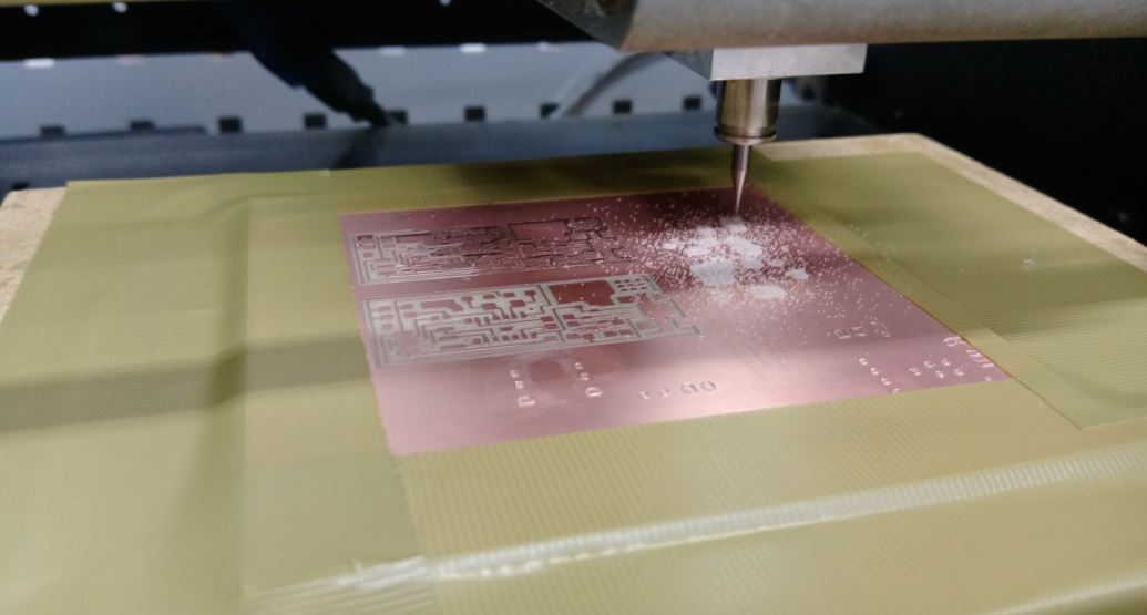
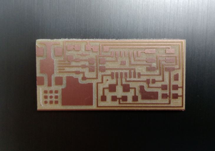
figure 5: After changing the base board of the mechine, the milling result looks well.
● Soldering the components
In this part, It needed to solder carefully becauce all the components were SMD and quite small. I made two mistakes here. First, I did not consider about the pins of the usb connenter were too closed. So I broke one trace while soldering. Then I made a bridge between these two solder joints. Second, I did not notice the direction of the Zener diodes, and solder the wrong side of them. After reviewing the documentation which the student wrote last year, I found the mistake anf fixed it.
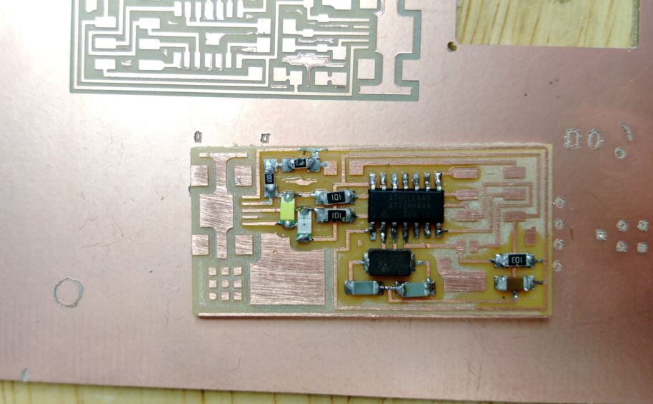
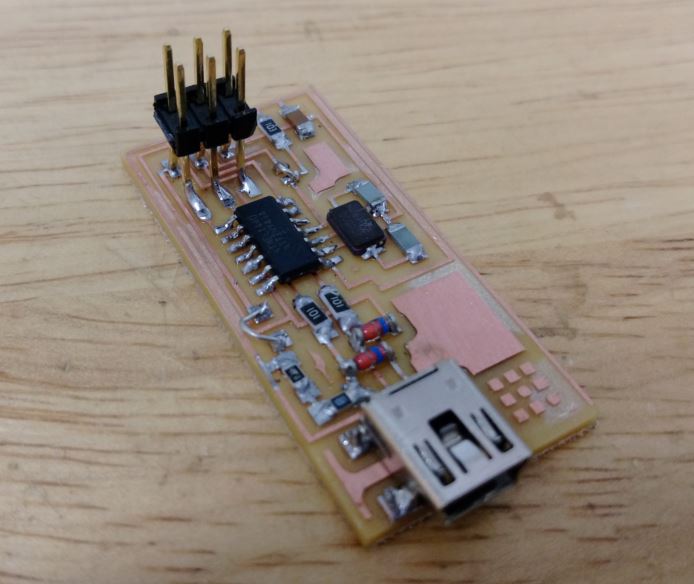
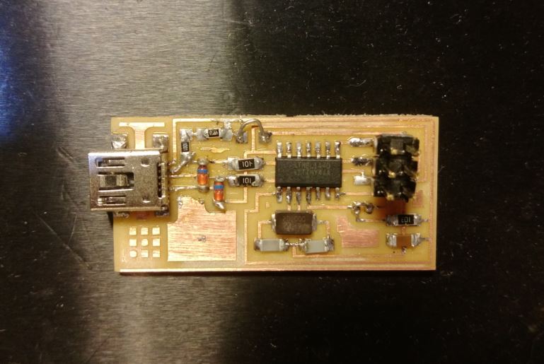
figure 6: Soldering the components.
● Programming the FabISP
By reading the Fab academy tutorials, I had the concept about programming the FabISP. First, I downloaded "Atmel Studio 7" as my programming tool, and used the AVRISP MAKII as the programmer. So I just needed to make sure the connection between AVRISP MKII and FabISP was corrected. Second, I downloaded the firmware from the website of Fab academy classes. Third, on the Atmel Studio 7 GUI, just went to "tools->Device management", and selected the suitable parameter on "tool", "Device" and "Interface", then pressed the "Read" button, It would show the "Decive Signature" and "Target Voltage" of FabISP. Then went to the "Memories" page, choosed the proper firmware hex file and press the "Program" button and it would directly do the "erase", "program" and "verify" procedures and showed the result on the message area below.
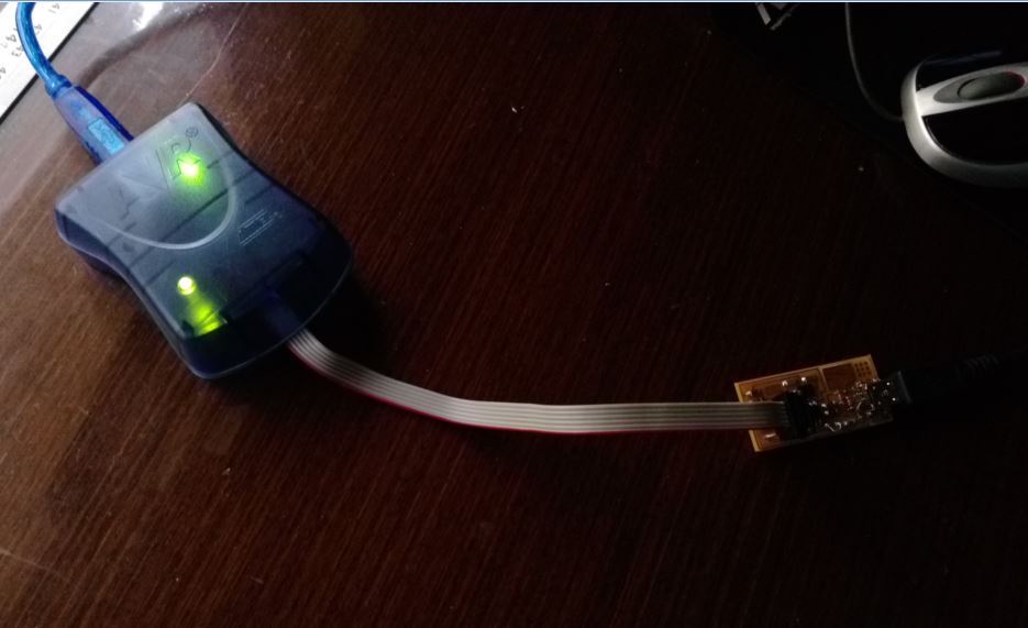
figure 7: AVRISP MKII.
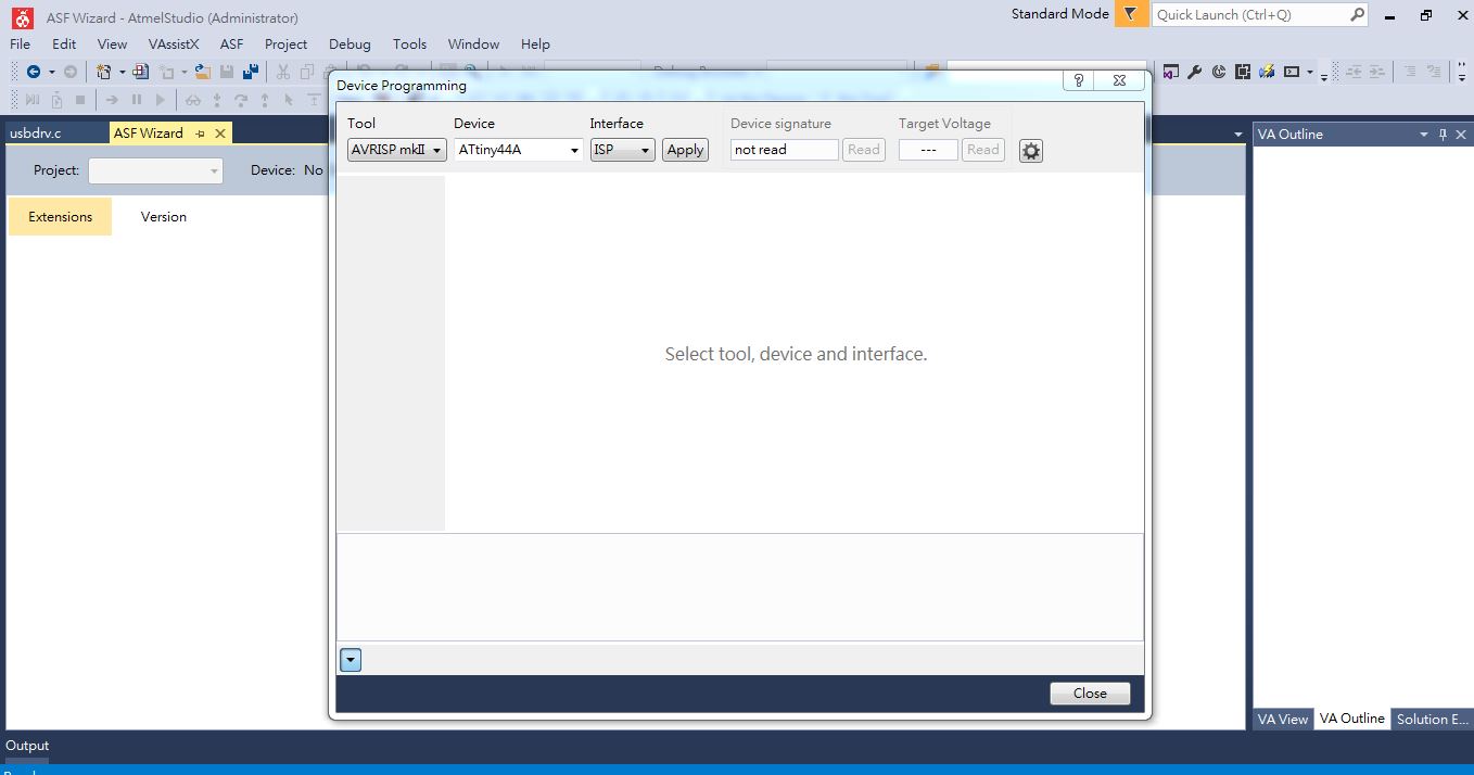
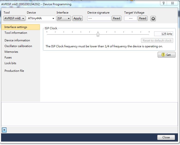
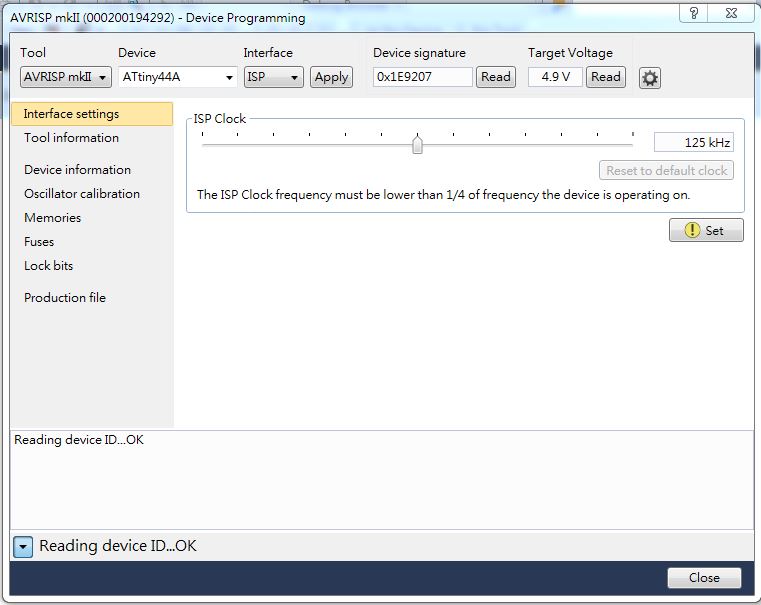
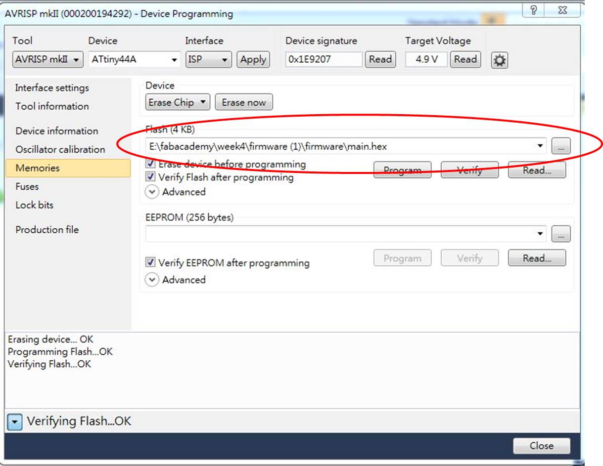
figure 8: Programming with Atmel Studio 7.
Then I download the USBtinyISP driver "adafruit_drivers" to intall the FabISP which was programed. I found that the FabISP was programed well, but my computer could not identify it. So I reviewed some documentations which wrote before, then I doubted if I used the different firmware. I downloaded another version of firmware and tried the procedures above again and it worked.
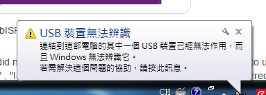
figure 9: My computer could not identify the FabISP after programming .
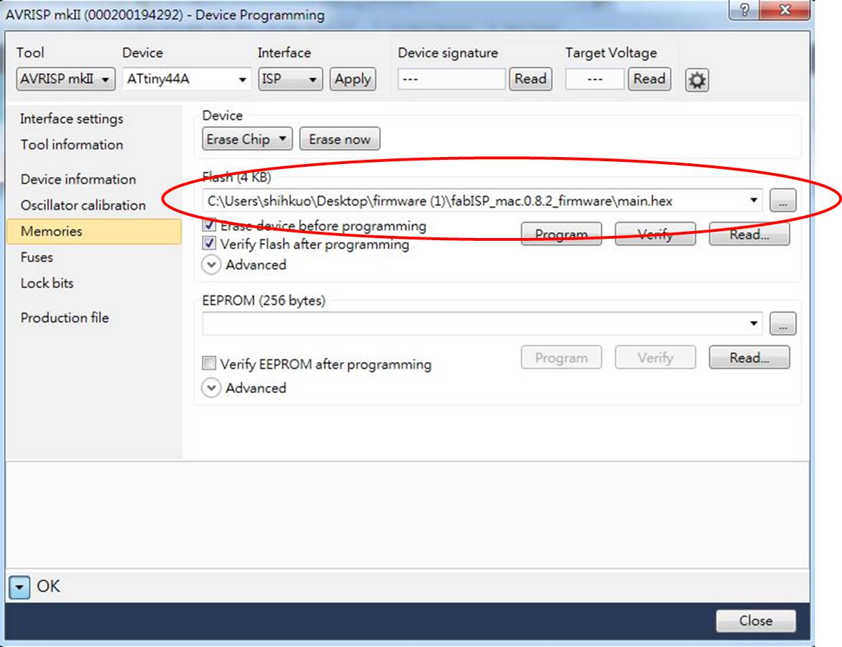
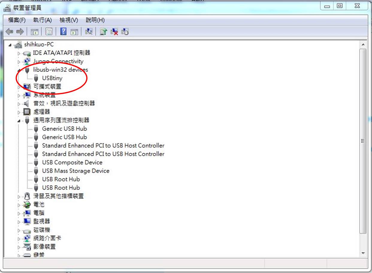
figure 10: After changing another firmware and redoing programming process, it was succeed.
But it is strange that my computer recognize the board as USBtiny, so I try to program it again with another way.
I program the board on mac computer, and use arduino uno as ISP.
The connection between FabISP and arduino is as follow :
arduino pin 10 --> FabISP RST
arduino pin 11 --> FabISP MOSI
arduino pin 12 --> FabISP MISO
arduino pin 13 --> FabISP SCK
arduino pin 5V --> FabISP VCC
arduino pin GND --> FabISP GND
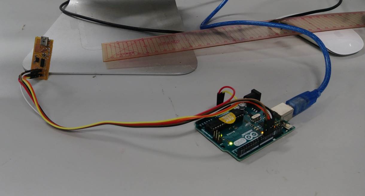
figure 11: Connection between FabISP and arduino.
At the first, I need to find the connection port of arduino. So start the Arduino IDE, check Tools --> Port, and find the port is /dev/cu.usbmodem1451.
Download fabISP_mac.0.8.2_firmware (firmware.zip) from class lectures and unzip on Desktop. Open Makefile from fabISP_mac.0.8.2_firmware, and
add a line below and save :
AVRDUDE = avrdude -c stk500v1 -b19200 -P /dev/cu.usbmodem1451 -p $(DEVICE)
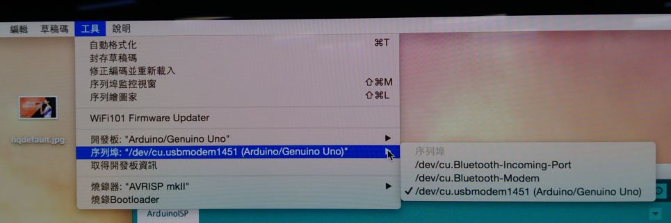
figure 12: The connection port of arduino.
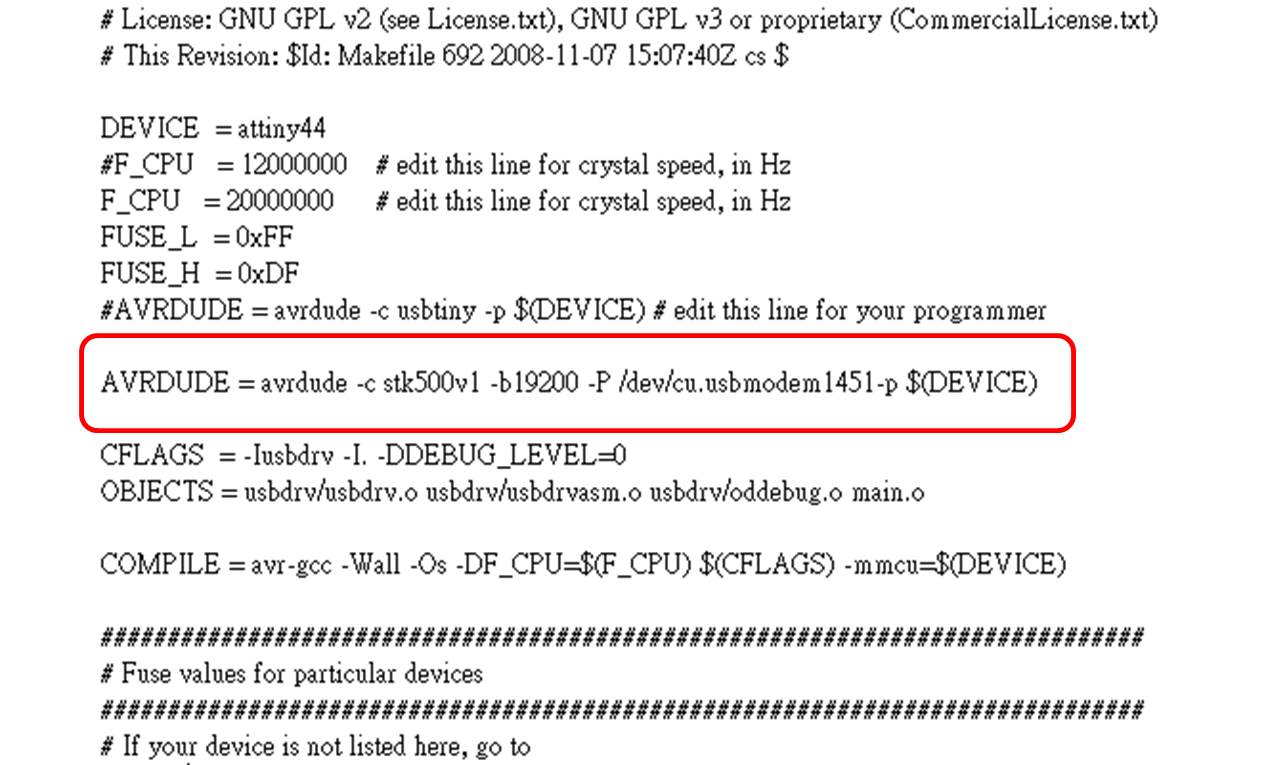
figure 13: Add the line on the makefile.
Open the terimal on mac computer, after finding the location of the fabISP_mac.0.8.2_firmware, type the command make clean, make hex, make fuse and make program.
$ cd Destop/
$ cd fabISP_mac.0.8.2_firmware/
$ make clean
$ make hex
$ make fuse
$ make program
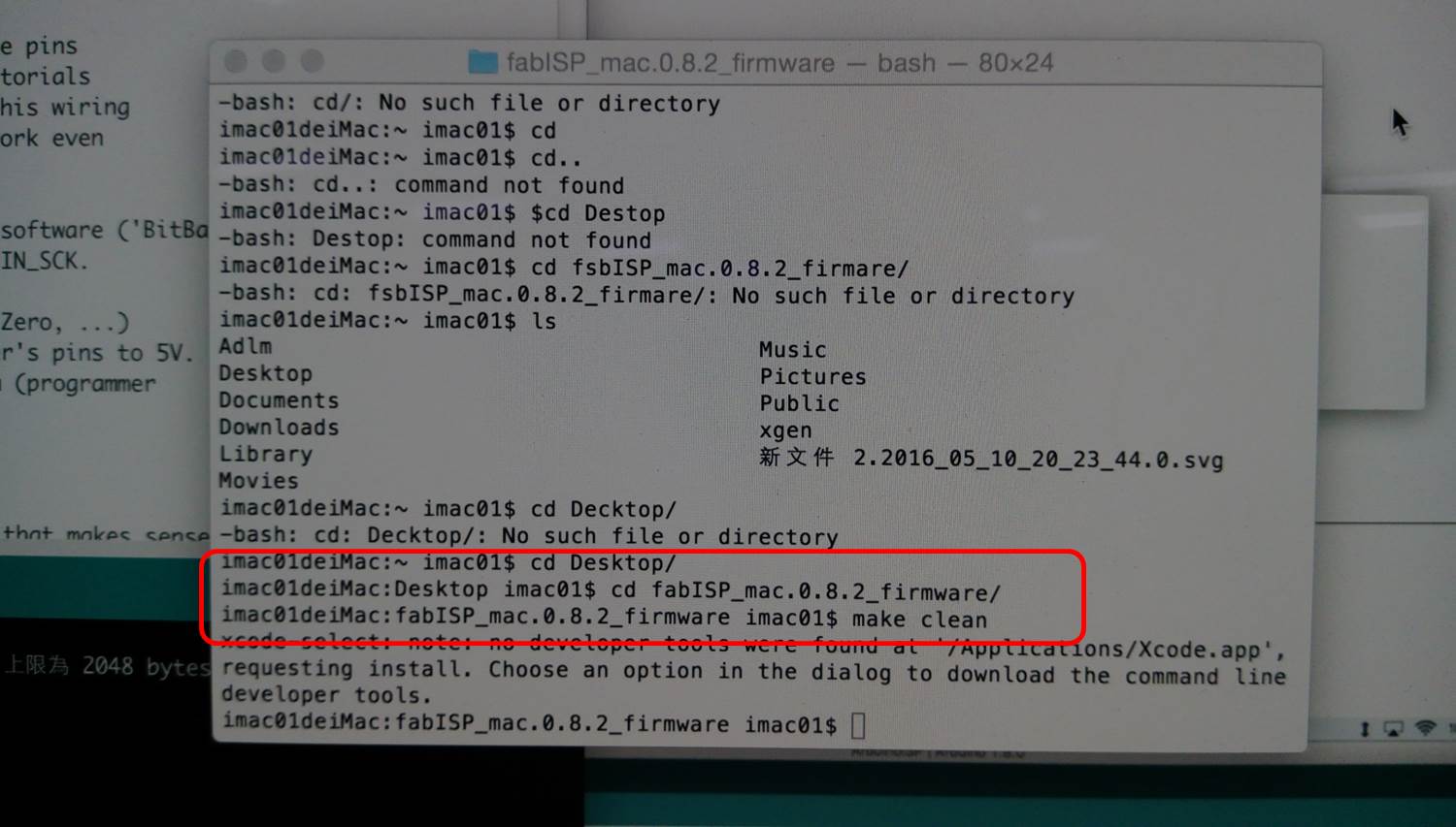
figure 14: make clean.
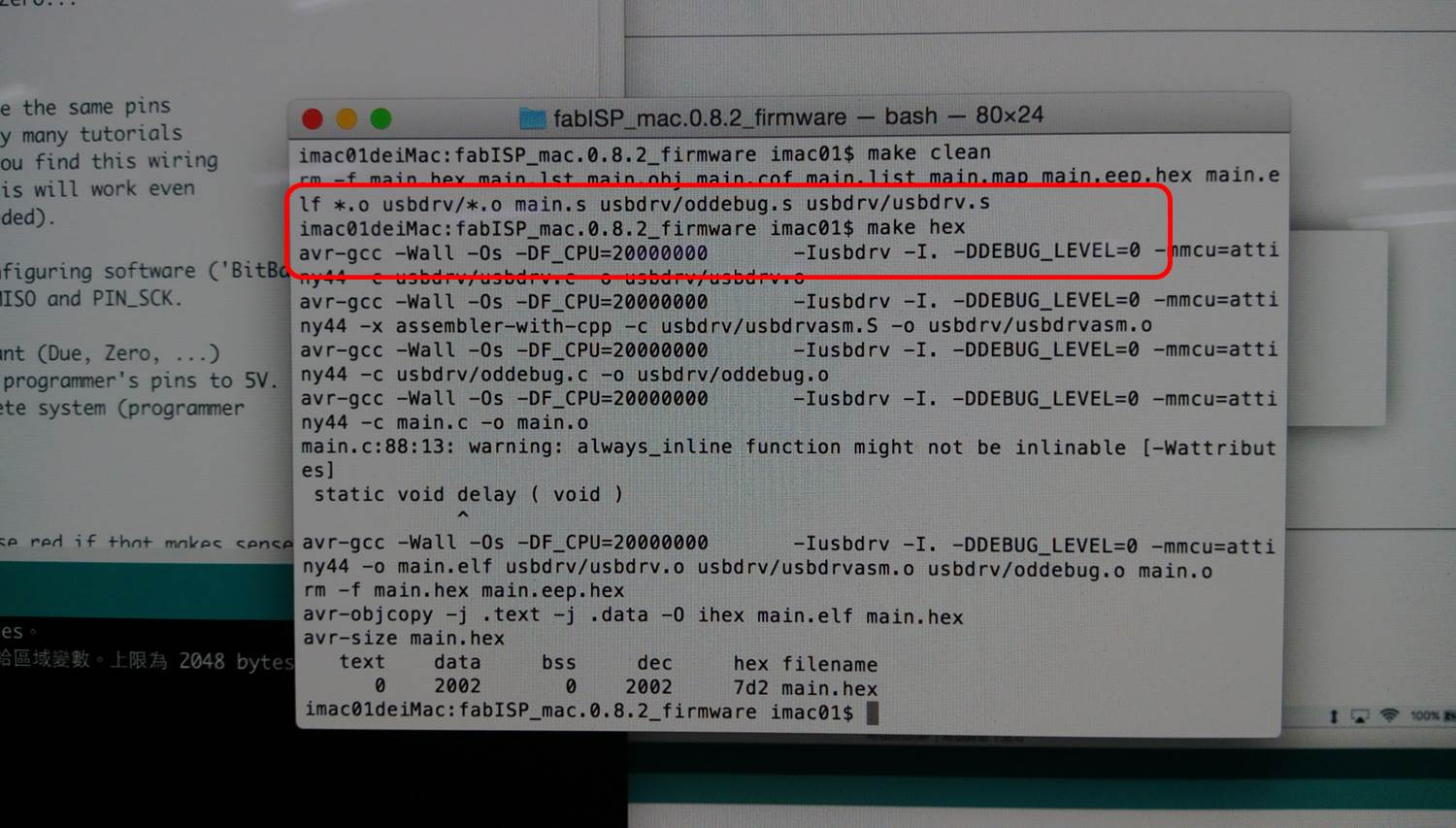
figure 15: make hex.
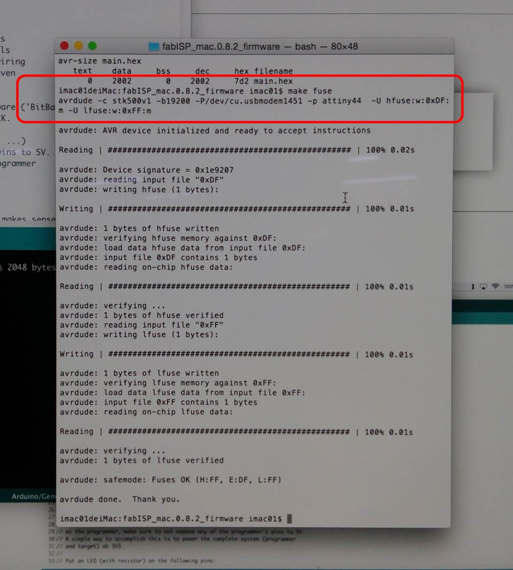
figure 16: make fuse.
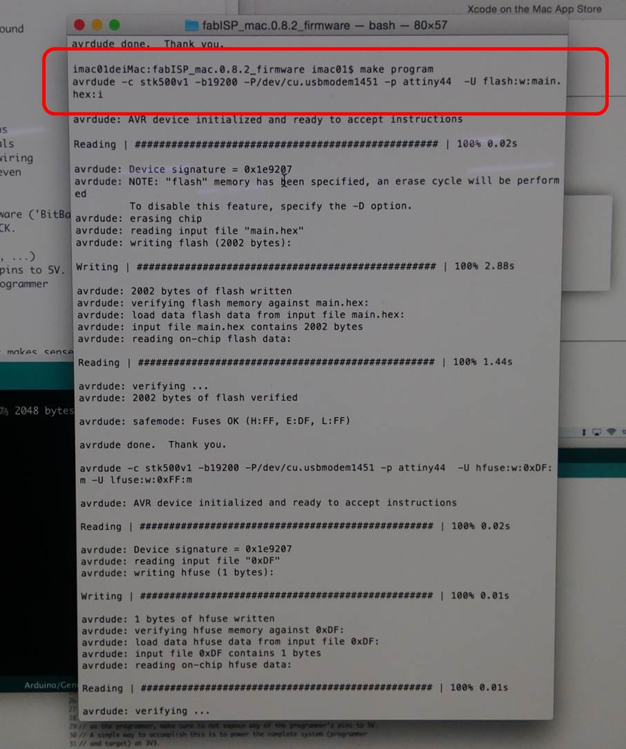
figure 17: make program.
After finishing these steps, I verify the FabISP from the computer, and it recognize the board as arduino uno.
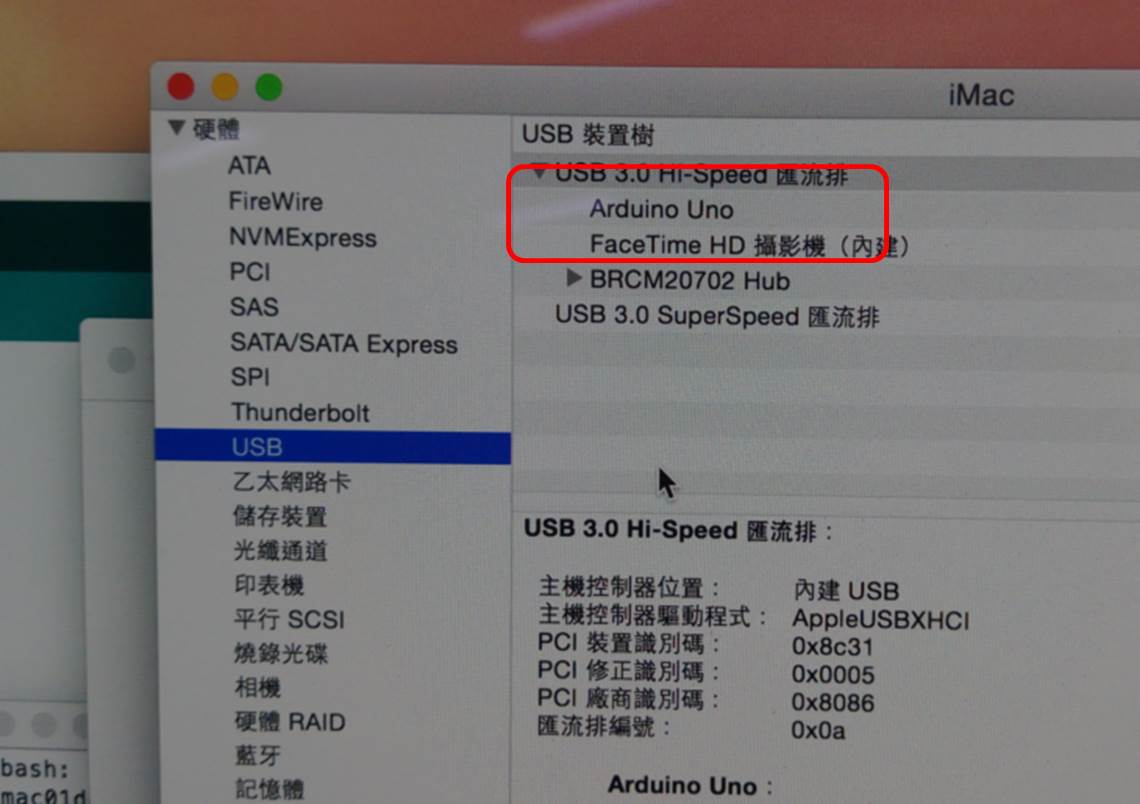
figure 18: Computer recognizes the board as arduino uno.
The final step is to remove the jumper SJ1 and SJ2, and Computer finally recognizes the board as FabISP. I got my FabISP.
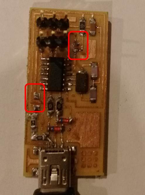
figure 18: Remove the jumper SJ1 and SJ2.
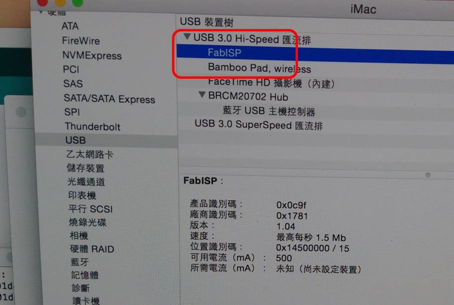
figure 19: Computer recognizes the board as FabISP.
● Source file
1.Png file of FabISP traces.
2.Png file of FabISP interior.
3.Firmware.