Electronics production
Assignment
Make an in-circuit programmer by milling the PCB, then optionally trying other processes
Brian Zaerc Ali Valentin Andy David
hello.ISP.44.cad board components traces interior
hello.ISP.44.res.cad board traces interior
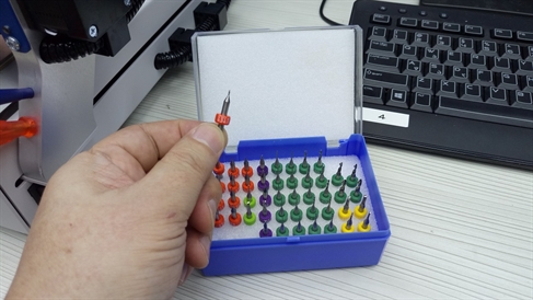
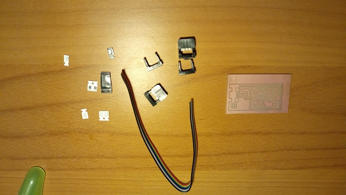
inventory microcontroller crystal USB connector ribbon connector Zener diode jumper
firmware.zip
USB power
make clean
make hex
(sudo) make fuse (check programmer in Makefile, may need to repeat)
(sudo) make program
desolder SJ1 and SJ2
make IDC ISP cable, connecting header pin 1 to pin 1, check wires
programming
Make an in-circuit programmer by milling the PCB, then optionally trying other processes
Brian Zaerc Ali Valentin Andy David
hello.ISP.44.cad board components traces interior
hello.ISP.44.res.cad board traces interior
inventory microcontroller crystal USB connector ribbon connector Zener diode jumper
firmware.zip
USB power
make clean
make hex
(sudo) make fuse (check programmer in Makefile, may need to repeat)
(sudo) make program
desolder SJ1 and SJ2
make IDC ISP cable, connecting header pin 1 to pin 1, check wires
programming
Group Assignment
Mr Steven Chew and Mr Rodney Dorville,our gurus at SP@FabLab have been kind enough to guide us in detial in setting up the PCB ruouter for cutting the existing design hello.ISP.44 by Neil.
The process involves getting a PNG PCB board file into Eagle PCB tool, generate Gcode and run it on the PCB router.
Individual Assignment
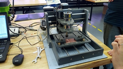
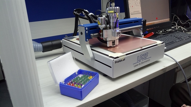
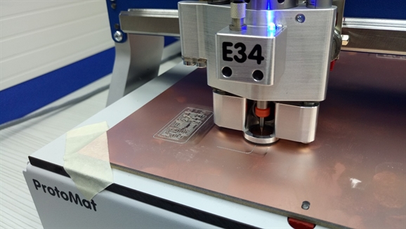
Back in Science Centre, our PCB cutting machine has finally arrived, it is a LPKF E34. I will be using this this machine from now onwards.
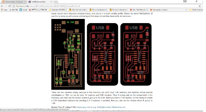
I normally build circuit using bread board, prototype board, wire wrapping and sometimes, etching PCBs. This is the first time I try to make PCB using a PCB router, in view of that, I don't intend to make any change to the circuitry. So I make use of the design from Ali Shtarbanov, I downloaded the schematic file plus board file from this site:
http://fab.cba.mit.edu/classes/863.16/doc/tutorials/FabISP/FabISP_Demystified.html
Here is the step by step procedure to produce a PCB.
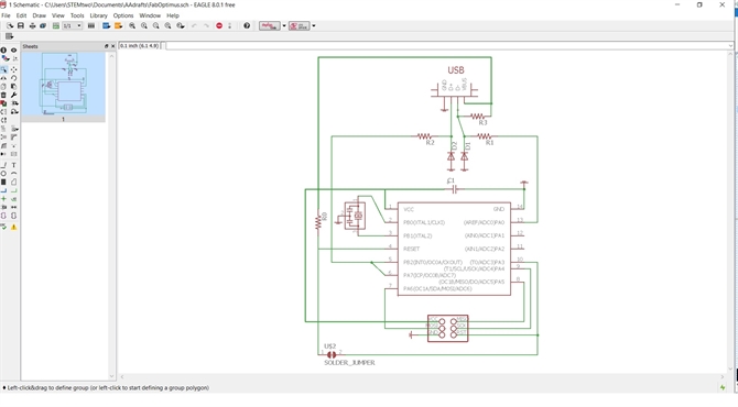
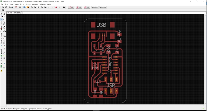
The first thing to do is to go to Eagle PCB tool, open the schematic file follow by the board file. Ali's design looks similar to hello.ISP.44 but it is using a ocsillator rather than a crystal plus 2 capacitors. It also uses the same microcontroller, the Attiny44. Both designs use USB connectors to replace the direct insert into USB ports.
There are also 2 jumpers SJ1 and SJ2. One for reset and the other for VCC. Both include 2 zener diodes to provide current flow protection.
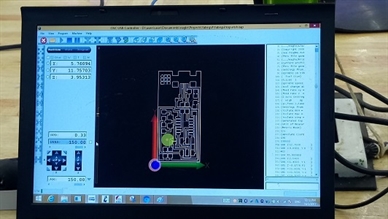
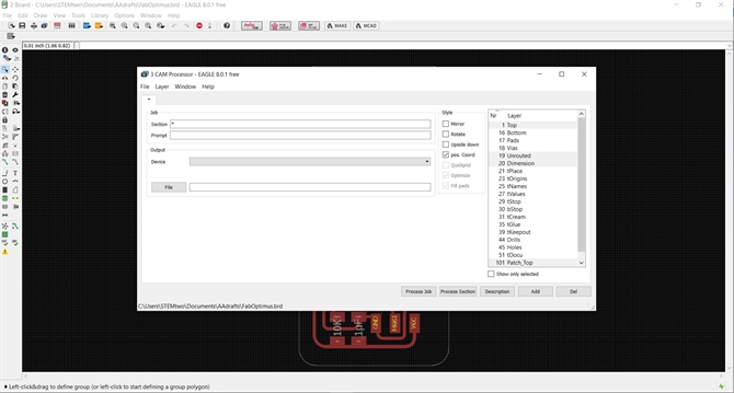
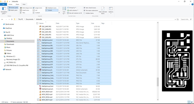
To get the PCB cut on the router, I need to generate a set of Gerber files. to do that, go to "File" -> "Cam processer" and a CAM processor window pops up. On the CAM processor window, go to "file" -> "open" ->"job", select the cam file "sfe-gerb274x.cam" (for this case because I am using the sparkfun Gerber Generating Cam Processor). Click the button "Processing job" at the bottom and a set of Gerber files will be generated.
Go to the directory where board file is stored and the gerber files are there. copy these file to a thumb drive and go to the PCB router
PCB routing
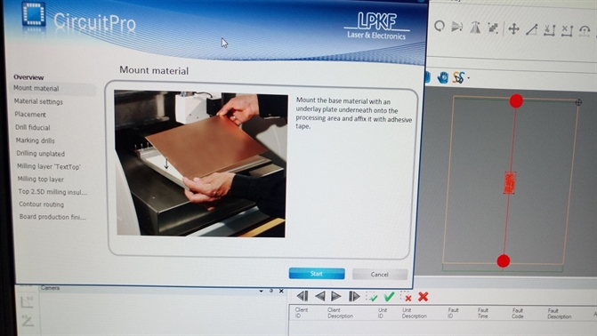
The LKPK E34 PCB router
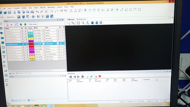
Launch the PC appliocation "Circuit Pro PM".
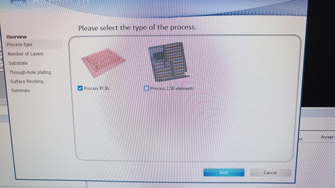
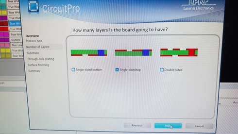
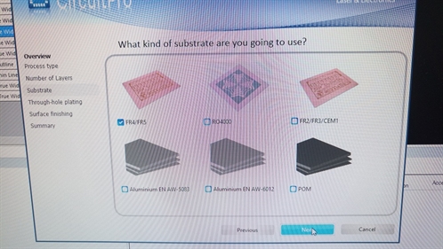
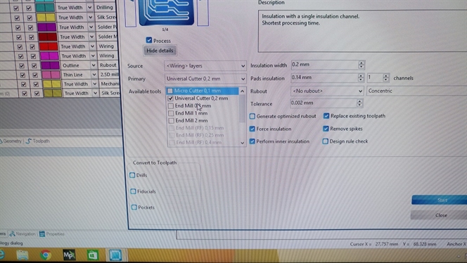
Select type of job to be carried out, in this case, it is "Process PCB" for top layer only, that is the "Single layer top". Then select the type of material used, in this case I am using FR4, so "FR4/FR5" should be selected.
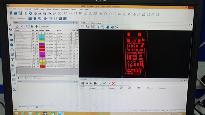
After that, load the gerber files into Ciruit Pro PM, in my case, only the top layer and outline are required.
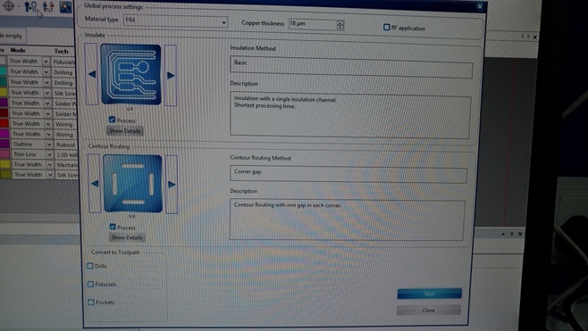
Set the Pads Insulation distance to 0.3mm from 0.02 to give a wider gap between solder pads, this is important to ensure less likelihood of shorting during soldering.
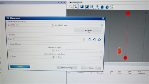
Place a piece of PCB material on the cutting table, make sure it is aligned to the guide pins at the top and bottom of the PCB material. define an area at the bottom left corner for cutting.
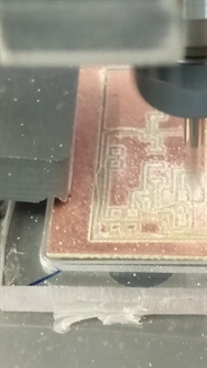
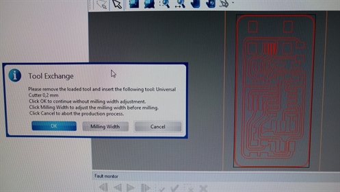
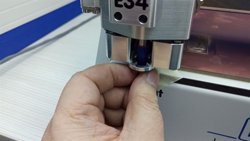
Continuing on, the machine will prompt you to install 0.2mm cutting tool on the spindle. this is the only tool I will be using. Although the machine is able to route the outline of the PCB, the cutting tool required for this purpose is not available.
The cutting starts after the button "contrinue" is clicked.
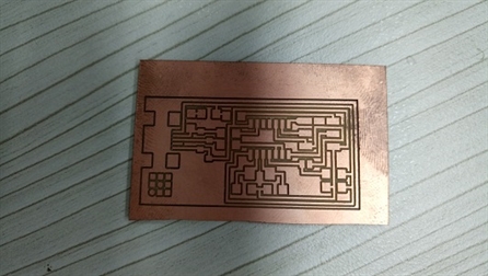
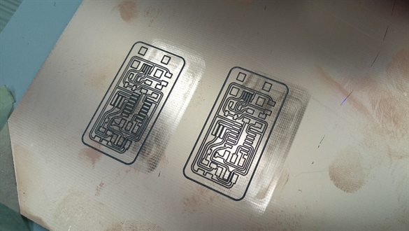
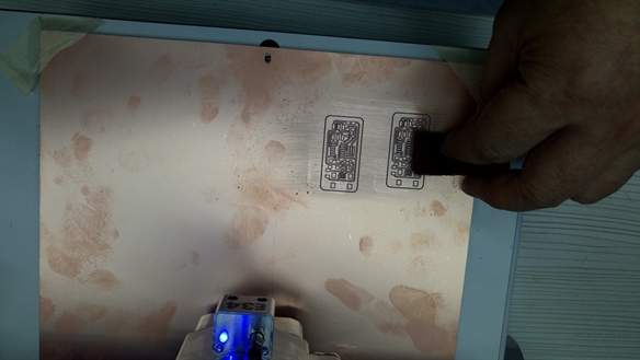
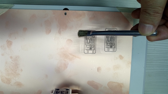
When cutting is done, inspect to see if there is any visible evidence of over or under cut like blur or broken trace.
If it is ok, brush the surface with an abrasive sponge and clear the dust with a brush.
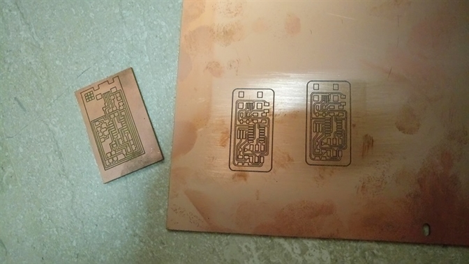
Next is to cut out the PCB manually.
Assembling
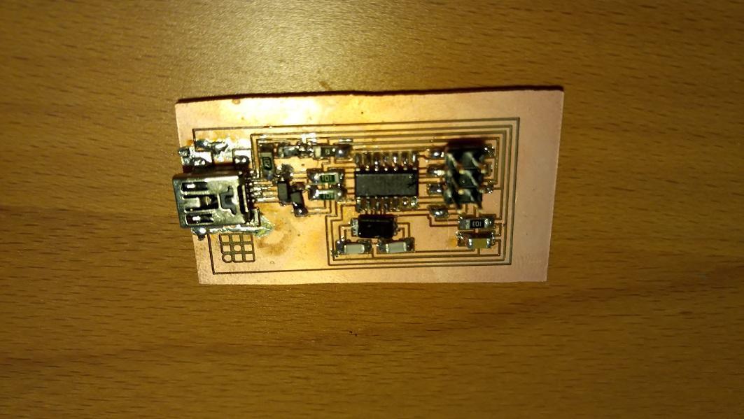
There are now 2 type of PCBs I can use for assembly, the hello.ISP.44 from group assignment and the one I just made.
Since the set of components given include a crystal and 2 capacitors, not a oscillator required for the Ali Shtarbanov's design, I go for the first one.
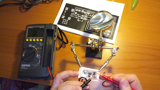
Before proceeding to assembly, check the traces with a multimeter to make sure that there is no short to ground from the VCC pin.
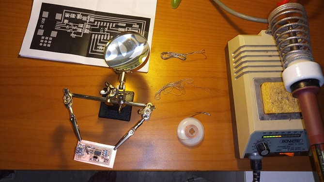
Next is to look at the component placement carefully and decide which component to solder first, work out the sequence so that you will not be obstructed by the previously installed components. Otherwise there could be some removing and resoldering.
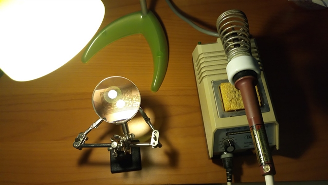
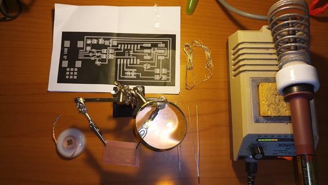
For SMD component soldering, a fine tip soldering iron with temperature control is recommended. Place the PCB on a sturdy stand. Magnifying glass, lighting, tweezer, solder wick and wet sponge for cleaning the solder tip are also required.
Make sure the diagram for component placement is also at hand.
There are now 2 type of PCBs I can use for assembly, the hello.ISP.44 from group assignment and the one I just made.
Since the set of components given include a crystal and 2 capacitors, not a oscillator required for the Ali Shtarbanov's design, I go for the first one.
Before proceeding to assembly, check the traces with a multimeter to make sure that there is no short to ground from the VCC pin.
Next is to look at the component placement carefully and decide which component to solder first, work out the sequence so that you will not be obstructed by the previously installed components. Otherwise there could be some removing and resoldering.
For SMD component soldering, a fine tip soldering iron with temperature control is recommended. Place the PCB on a sturdy stand. Magnifying glass, lighting, tweezer, solder wick and wet sponge for cleaning the solder tip are also required.
Make sure the diagram for component placement is also at hand.
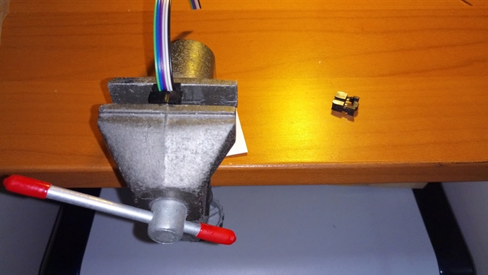
The 3x2 flat cable can be assembled using a table clamp as shown, just make sure that the cable are aligned properly before closing the clamp.
When the soldering is done, do not connect the power and program the Attiny44 chip immediately. Again use a multimeter to check to make sure there is not short to ground.
Check electrical continuity between Vcc and Gnd on the 3x2 header. then the Vcc and Gnd on the USB connector pins. These are important checks before powering up the board to aviod any smoky episode.
Next check all the connections between 3x2 header and the Attiny44 microcontroller pins.
With all that Done, the board is ready for programming.
Programming
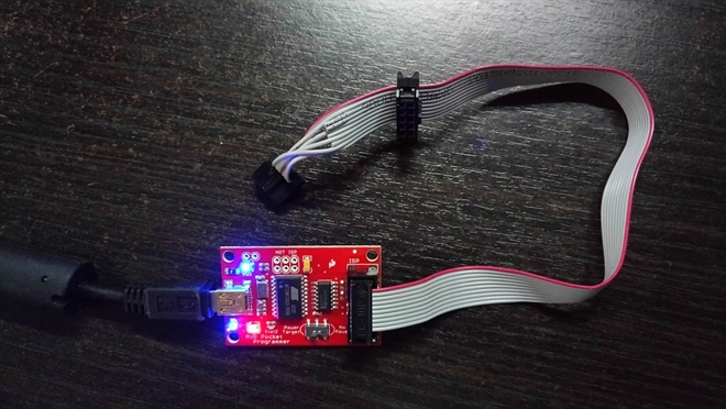
The programmer I am using is a Sparkfun Pocket AVR programmer, it is USBtiny programmer supported by AVRDUDE and comes with a 10 pin and 6 pin connectors.
Use the 6 pin connector to connect to the FABISP and connect the Pocket AVR programmer to a USB port on the PC.
The programmer I am using is a Sparkfun Pocket AVR programmer, it is USBtiny programmer supported by AVRDUDE and comes with a 10 pin and 6 pin connectors.
Use the 6 pin connector to connect to the FABISP and connect the Pocket AVR programmer to a USB port on the PC.
AVRDUDE
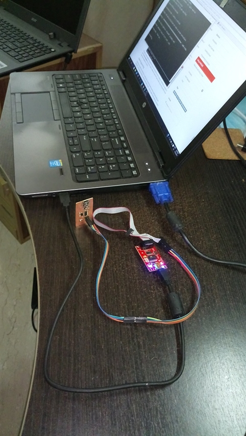
Since WINAVR is not very well supported. I decided not to install it on my PC. I will use AVRDUDE directly. There is a main.hex in the downloaded firmware folder but I am not sure it is the latest, so the Hex file required is copied from my colleague's Mac Book using Crosspack AVR with the Make Hex command.
AVRDUDE is a low level command line programming software. to use it under Windows, a command prompt window has to be opened.
The type of programmers, type of microcontrollers AVRDUDE supported and its command syntax can be found from the following web site:
http://www.nongnu.org/avrdude/user-manual/avrdude_4.html#Option-Descriptions
Open a command prompt window, go to the AVRDUDE directory, key in the following command:
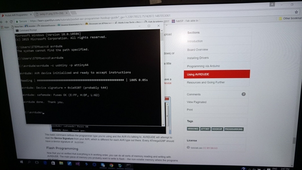
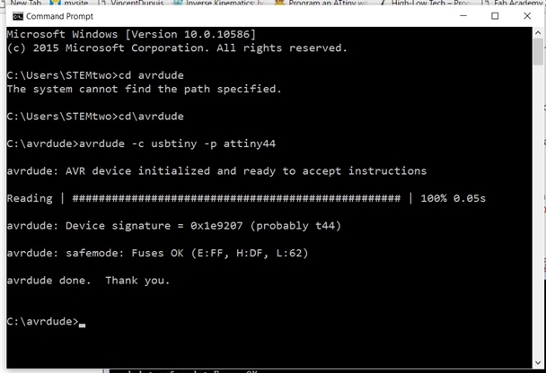
avrdude c usbtiny -p attiny44
If you see "AVR device initialised and ready to accept instruction", it means that the Pocket AVR programmer is able to access the attiny 44 microcontroller. All is well so far.
From the makefile provided, to load program to
Attiny 44:
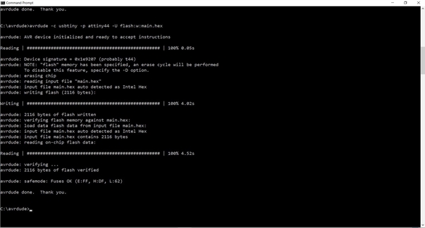
avrdude c usbtiny -p attiny44 -U flash:w:main.hex
If you see the display shown, the program loading is successful.
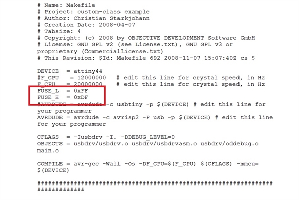
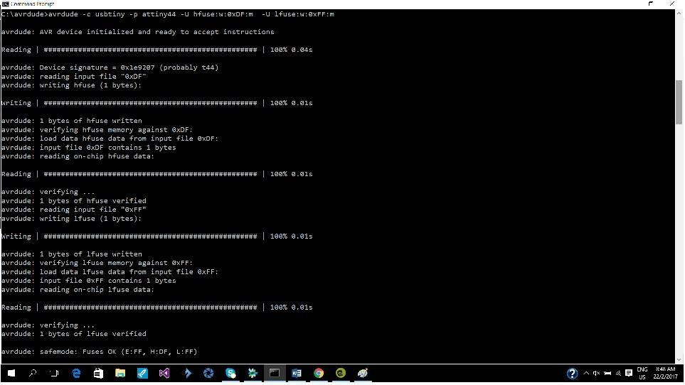
From the makefile again, to use the external crystal, the lfuse and hfuse should be set to 0xFF and 0xDF respectively. To load the fuse configuration to Attiny44:
avrdude -c usbtiny -p attiny44 -U hfuse:w:0xDF:m -U lfuse:w:0xFF:m
Since WINAVR is not very well supported. I decided not to install it on my PC. I will use AVRDUDE directly. There is a main.hex in the downloaded firmware folder but I am not sure it is the latest, so the Hex file required is copied from my colleague's Mac Book using Crosspack AVR with the Make Hex command.
AVRDUDE is a low level command line programming software. to use it under Windows, a command prompt window has to be opened.
The type of programmers, type of microcontrollers AVRDUDE supported and its command syntax can be found from the following web site:
http://www.nongnu.org/avrdude/user-manual/avrdude_4.html#Option-Descriptions
Open a command prompt window, go to the AVRDUDE directory, key in the following command:
avrdude c usbtiny -p attiny44
If you see "AVR device initialised and ready to accept instruction", it means that the Pocket AVR programmer is able to access the attiny 44 microcontroller. All is well so far.
From the makefile provided, to load program to
Attiny 44:
avrdude c usbtiny -p attiny44 -U flash:w:main.hex
If you see the display shown, the program loading is successful.
From the makefile again, to use the external crystal, the lfuse and hfuse should be set to 0xFF and 0xDF respectively. To load the fuse configuration to Attiny44:
avrdude -c usbtiny -p attiny44 -U hfuse:w:0xDF:m -U lfuse:w:0xFF:m
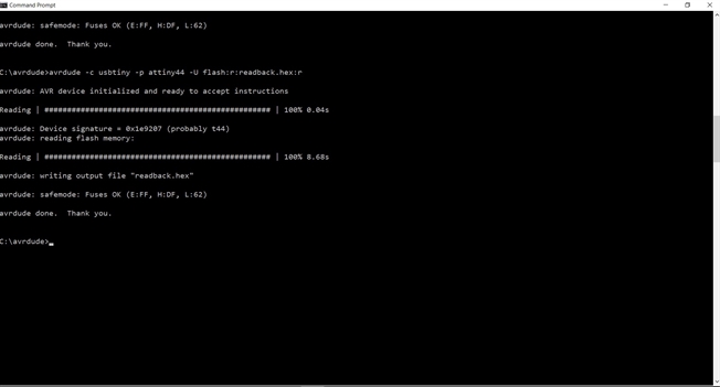
You can also do a read back from the microcontroller:
avrdude c usbtiny -p attiny44 -U flash:r:readback.hex
This will create a hex file readback.hex in the AVRDUDE directory.
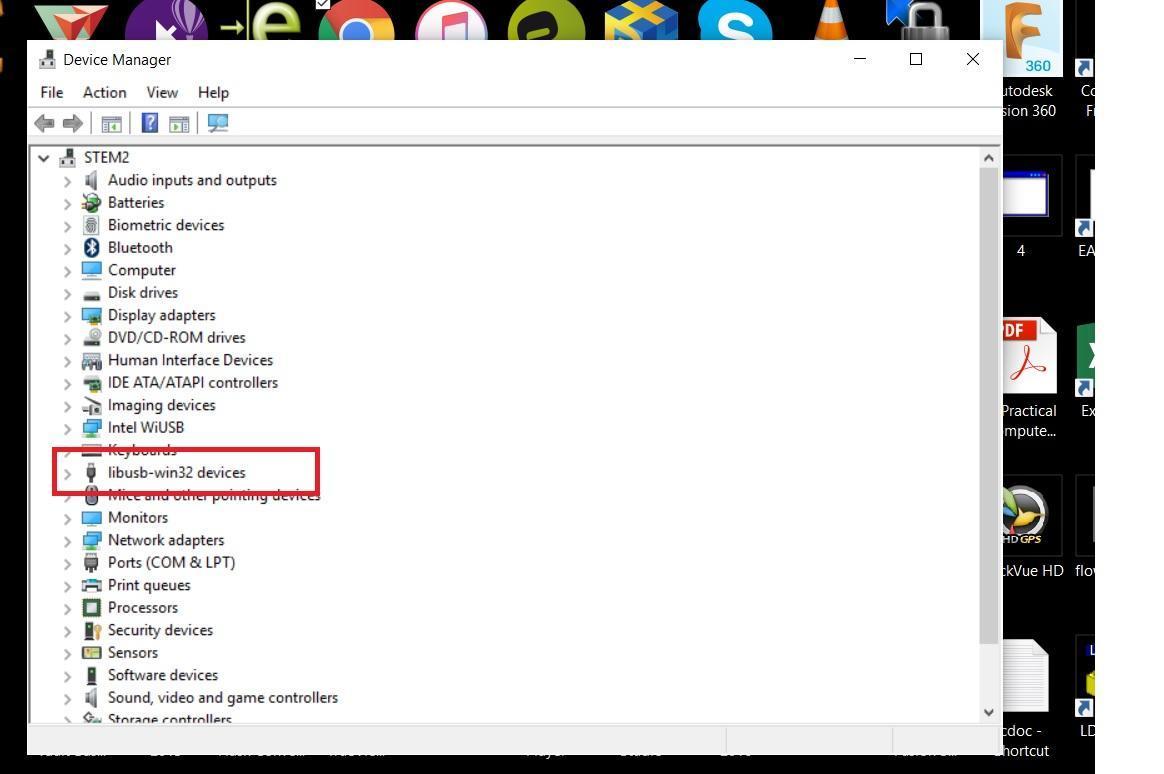
At this point. to prevent re-programming, the solder joints at SJ1 should be removed. SJ2 allows USB to supply power to the target via ISP connector. remove this means the target has to have its own power source.
Plug the FabISP into one of the USB port. if done correctly, at Device Manager screen, the FABISP should be listed as shown.
avrdude c usbtiny -p attiny44 -U flash:r:readback.hex
This will create a hex file readback.hex in the AVRDUDE directory.
At this point. to prevent re-programming, the solder joints at SJ1 should be removed. SJ2 allows USB to supply power to the target via ISP connector. remove this means the target has to have its own power source.
Plug the FabISP into one of the USB port. if done correctly, at Device Manager screen, the FABISP should be listed as shown.
Reflection
Making PCB via milling process is an environment friendly event when compares with chemical etching. In this assignment, I have learnt how to bring a Eagle PCB tool file to real PCB output.
The SMD components are smaller than the PTH components, soldering SMD requires steady hands and finer tools. An hot air reflow gun available at SP@FabLab is an effective tool for reworking.
The WinAVR was abandoned and I heard alot of problems installing it under windows. I did some looking around for gcc and avr-libc for Windows so that that I can compile the source code and generate Hex file. If not I will re-OS one of my old PC to Ubuntu in the future.