ELECTRONICS DESIGN
Circuit Design
I used Eagle to design this week's circuit.Thanks to Anna I was able to navigate through some of the challenging parts.In order to get some of the specific components that I needed for this assignment, I downloaded the fab lbr, FAB_Hello and Neil's ng libraries. I then added them to eagle by going to Control panel > Options > Directory > Libraries. Here you specify the folder in which the new library is located. Once you hit ok you are set to go!
So I started by importing all the components that I needed including Vcc and GND into my working space.
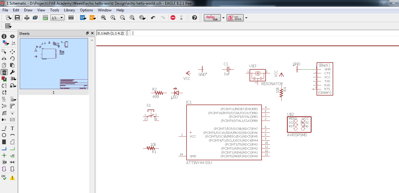
Number 2 step was to arrange them strategically according to the way I wanted them connected to each other I used the move tool to do that
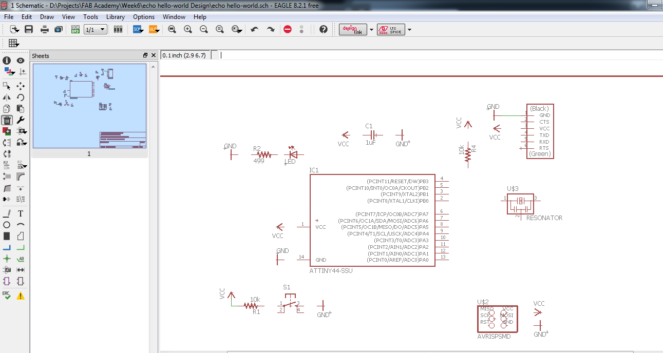
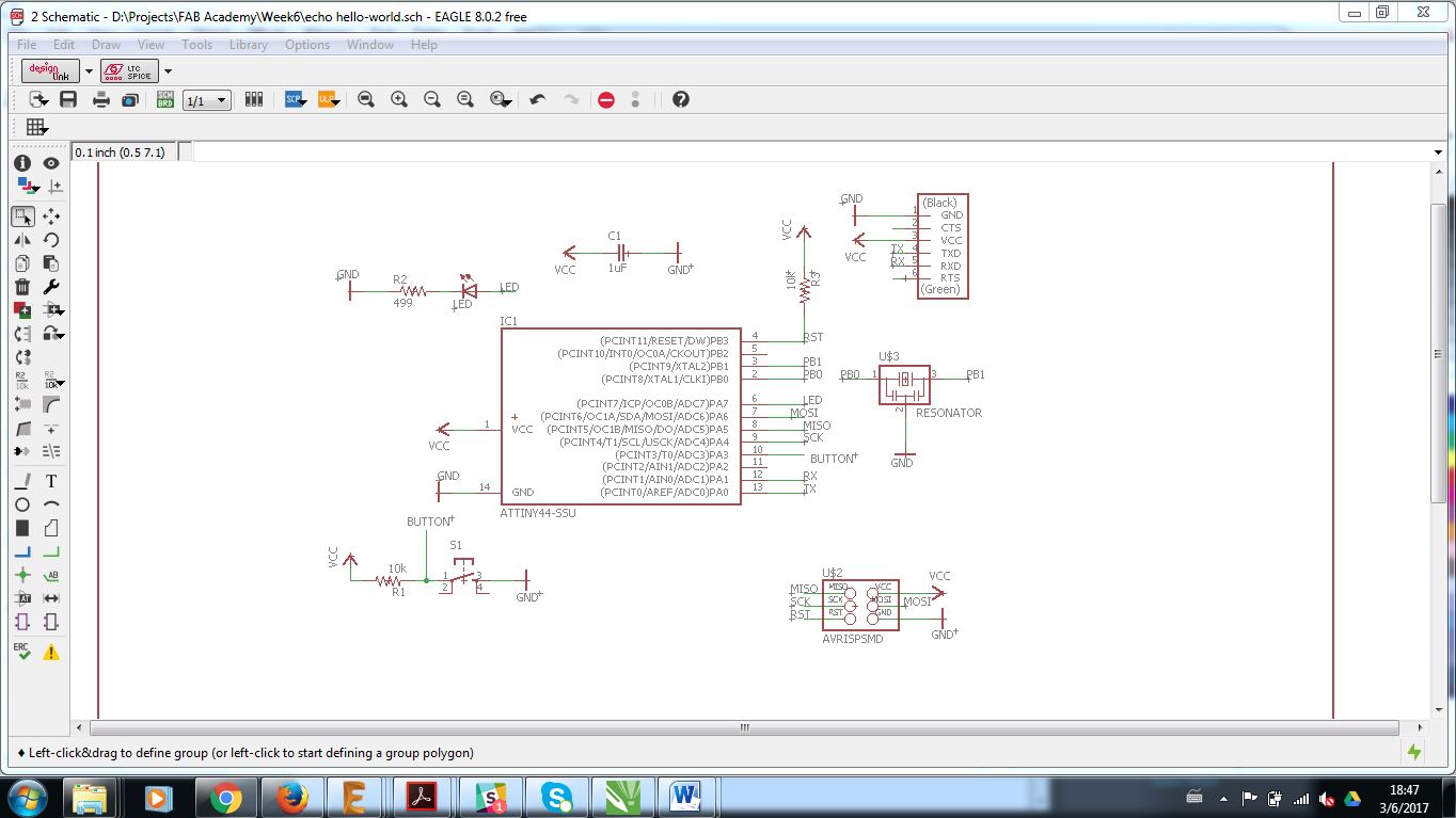
After that I used the line tool to connnect the components and later labelled them. At this point I as ready to get a board out of that design. I clicked on GENERATE/SWITCH TO BOARD
Here, all the components ad their connections were located outside the default workspace. I moved them insideone by one strategically locating them in a manner that will make it easier to route. I then routed them manually. The trace width is an important aspect of the board so I increased the width from default to 0.012. This would reduce the chances of having broken traces on the board during fabrication.I then routed the board on the TOP copper. While routing I also ensured that I had left enough spaces between the traces to avoid short circuiting
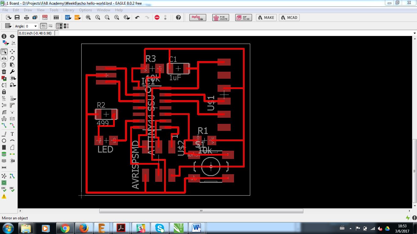
After this I had to confirm and make sure that the design has no errors. Towards the bottom left of the tools panel there is a tool called RATNEST. I clicked on Ratnest and the response I got was 'Nothing to do!'. I as pleased because then I knew that all the tracks had been completely routed.
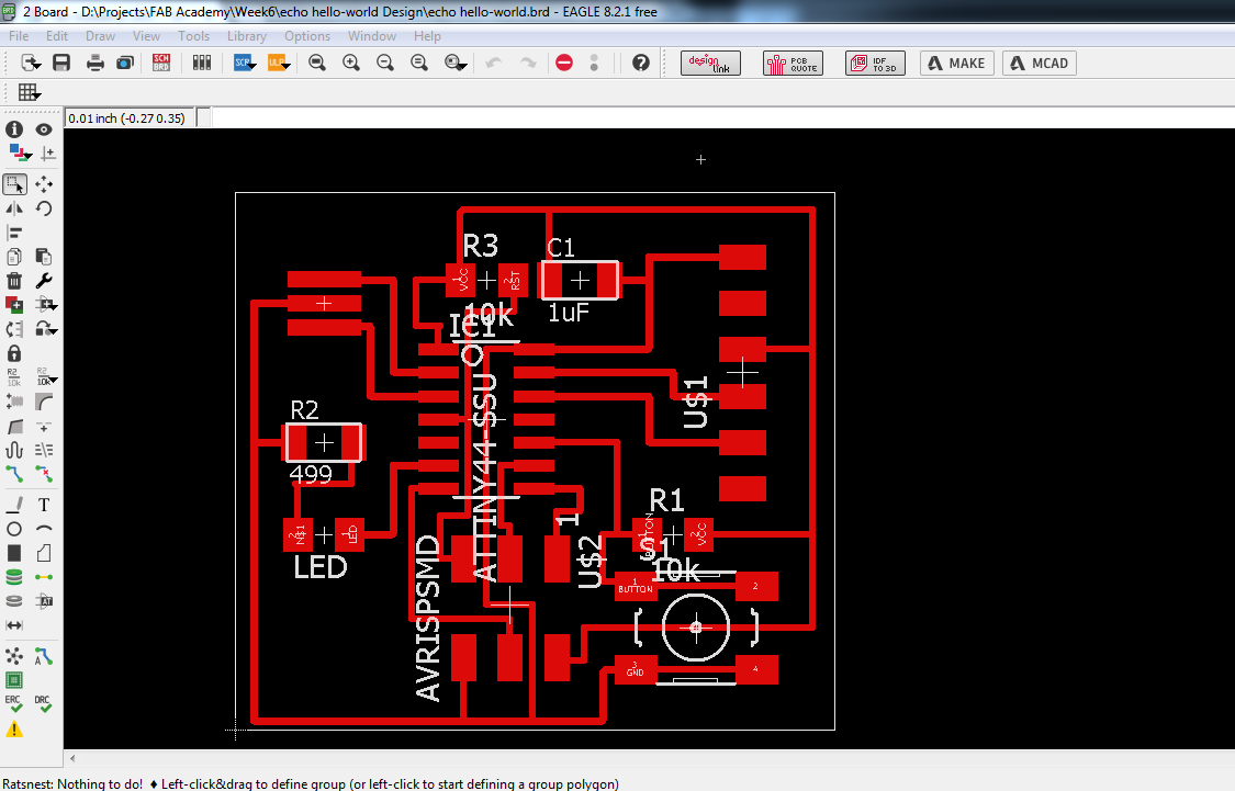
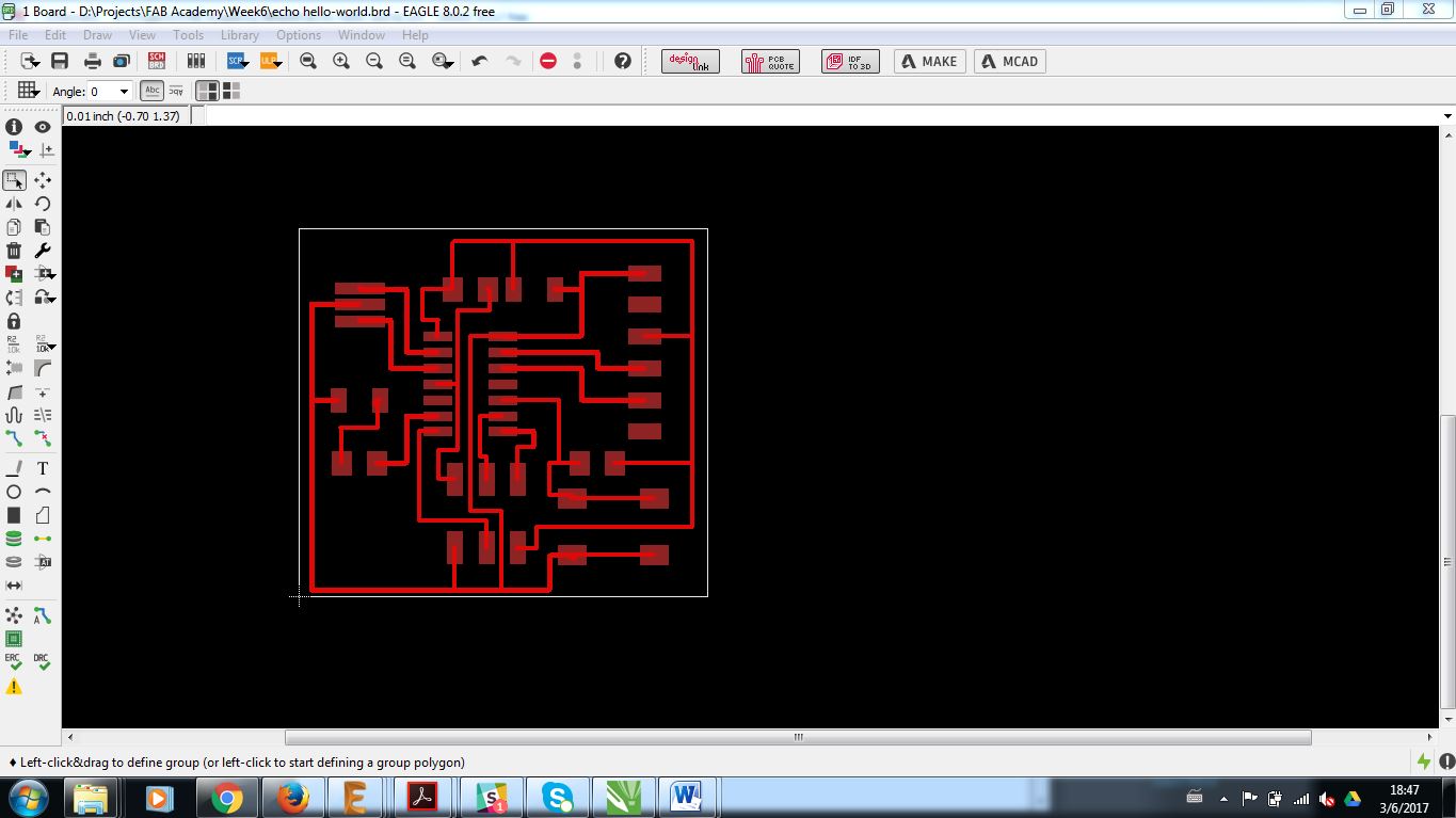
After that I was ready to export the board for milling. So I clicked on LAYER SETTINGS to get rid of the unnecessary details that are not needed on the board
Circuit Milling
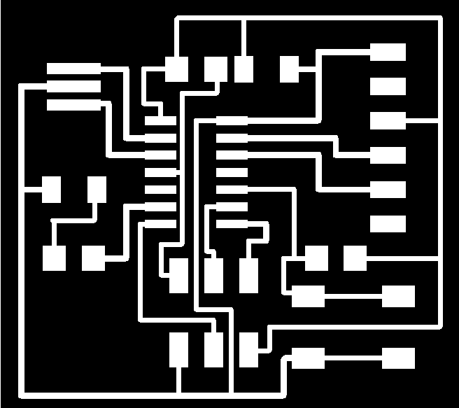
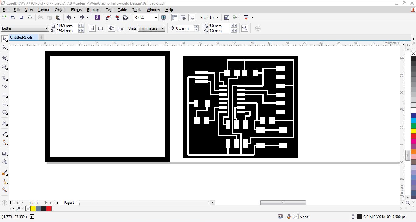
I exported the circuit in monochrome PNG format but the image turned out to be slightly larger than the size I needed for milling which should have been just withing the circuit margin I had defined. So I imported the png file to Corel Draw and trimmed it to size.
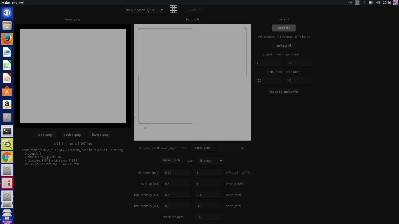
As for the interior, I drew a square shape around the earlier imported png then I trimmed it to be left with an outline. I colored it black and exported it in PNG format.
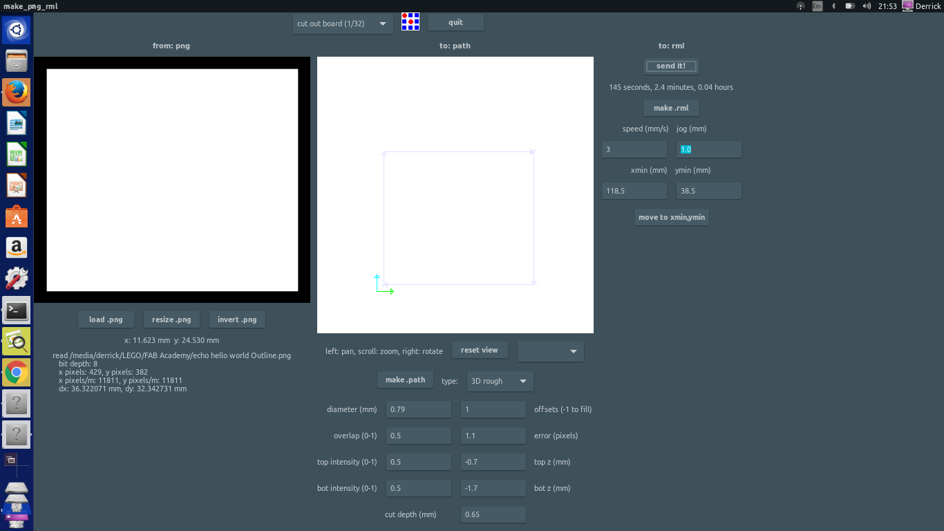
At this point I was ready for milling. I powered the Modela and set the xmin and ymin at 120mm and 40mm respectively, as that is generaly where my small piece of pcb board was located. I also set the Z-axis at value -0.15 and used a 1/64" bit for the job
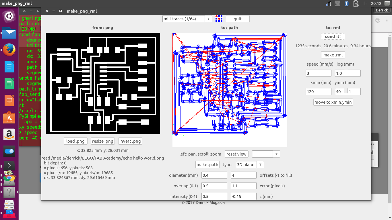
The first one was a test, whose milling went on very well right until I sent the interior image. Turns out my interior design was off by 1.5mm towards the right of the x-axis and 1.5mm off on the y-axis. It ended up cutting inside my nicely milled circuit and chipping off some of the copper traces.
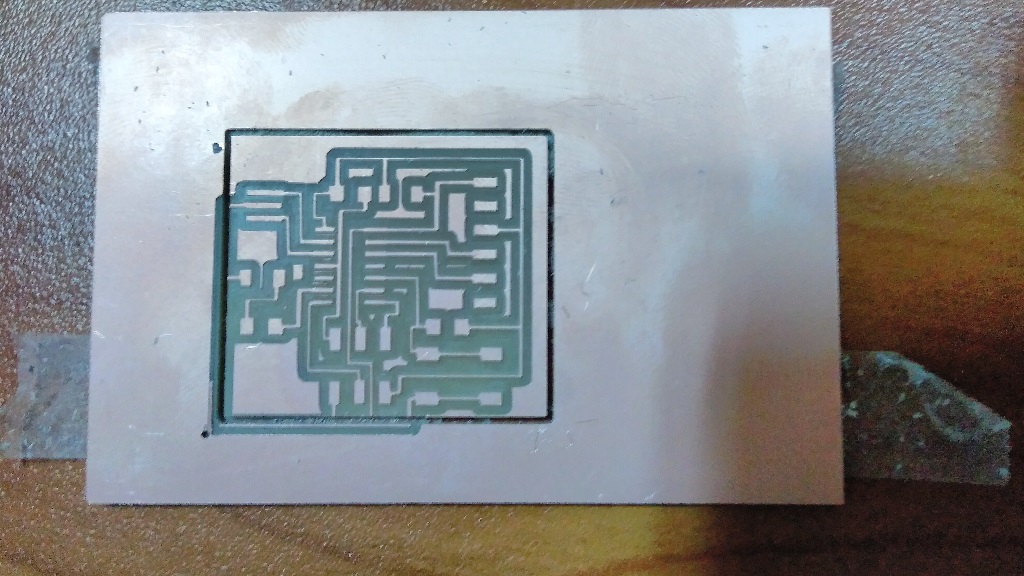
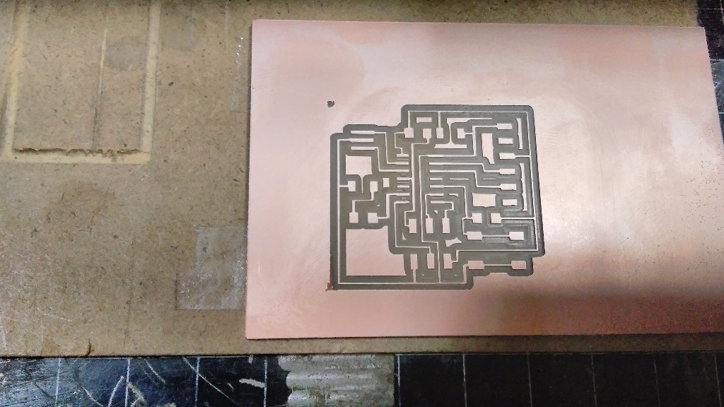
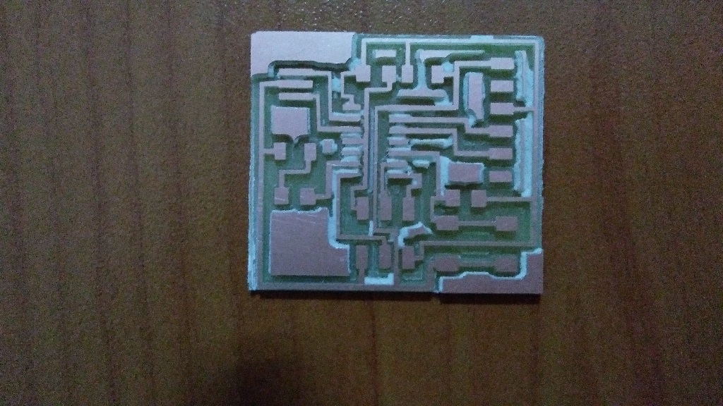
So I had to start milling a fresh circuit. This time, on uploading the interior image, I adjusted the Xmin and Ymin to 118.5mm and 38.5mm respectively to compensate for the error. This worked out well and I had my circuit well milled.
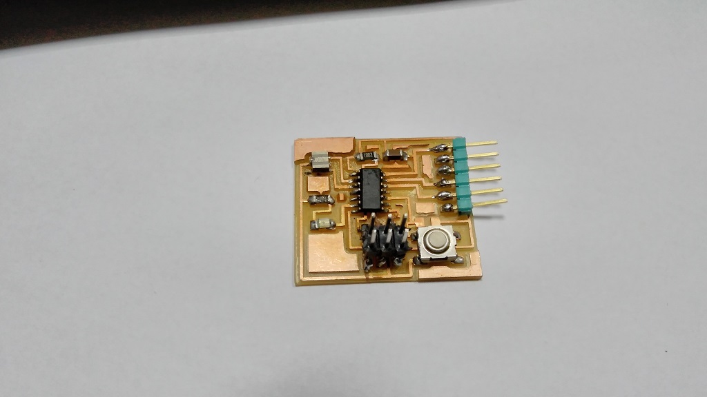
I then mounted the components and soldered them in place
Download files:
echo_hello_world.sch
echo_hello_world.brd