
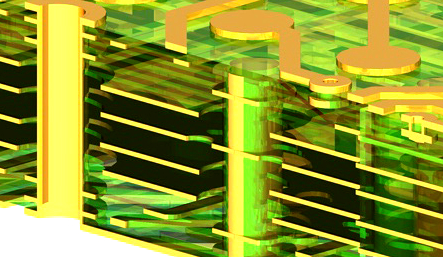
Circuit boards
In this week, I will create a circuit boards from schematic into printed circuit board (PCB). In week 4, there has been a shortcut to start with create the (PCB) immediately. But the previous step on drawing the schematic board was not the requirement. And this step is more important because I need to know what are my needs towards creating my project. In addition of the suitable choice of my preference. So this time, we will create the (PCB) from ground zero.
The history of PCB
In the old days, PCBs were not what we see nowadays. They were like components joined together with a point to point constructed method. At that time, people are facing difficult times due to the unorganized rotation designs, huge sockets needed and not applicable planning. With the years passed, the PCBs were developed and became more reliable.
1920s - PCBs was made from wood, drilled to make holes with wires attached into it. Not pretty.
1940s - PCBs began to be double sided boards.
1950s - Materials for PCBs are changing.
1960s - Wires now printed on one side and the electrical component on the other side which is better than 30 years before.
1970s - PCBs are using a color method for its components and tracks. Also boards and getting smaller.
1980s - Surface components are replaced other than holes with components.
1990s - The costs of PCB materials are decreasing. And the multi-layer circuit boards development is increasing.
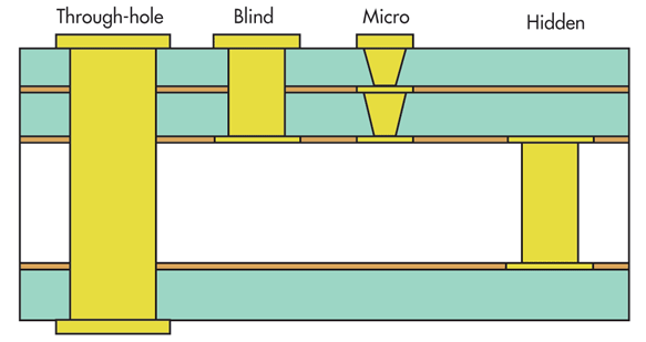
1995 - The production of PCB is the United States reached 7 billion dollars. In addition, the micro-via technology inside the PCB has started in production.
2000 - PCB fabrication in the United States market reached 10 billion dollars.
2010 - The new approach of ELIC (Every Layer Interconnect) now in production.
For more details:-
History of Circuit boards.Software
The program that I chose is called EAGLE. This software program helps generate schematics for PCBs, Board layouts and Arduinos. I preferred this program because it can create complicated boards and simple to use, also it has many features that I will explain. I have learned to make my first full schematic board to make the PCB with an LED and Switch on it for only 30 minutes. The demonstration on how to make one of those will be mentioned shortly.
Steps to make the Schematic Board
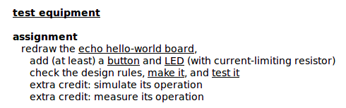
First of all, we will download the Equipment file from the Fablab archive.
The file called "echo hello-world board" under the test equipment section. Also we need to download the button and the LED to make the final test of the board if it works or not.
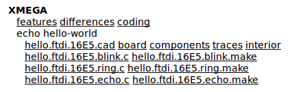
We have to have a trace board in order to know where to put the components on it. So we will also download that under XMEGA section.
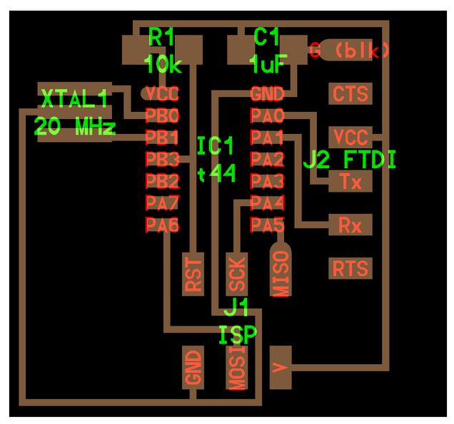
This is the trace map of the board. As we can see the routs and components how they are connected. This will be my guide for the whole process.
Once we have openned EAGLE, we need to add the Equipment file which we have downloaded from the Fablab archive to use it for the board. By using the Library on the top list and browse for the Fab file.
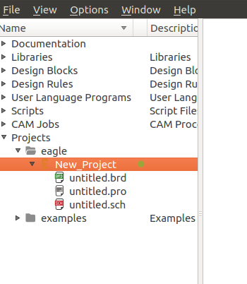
Now, we can start the project by pressing on new projects.
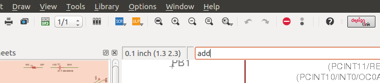
Once we have a new page, we now want to add the components on the white screen we see. First we will type "add" inside the text box on the top.
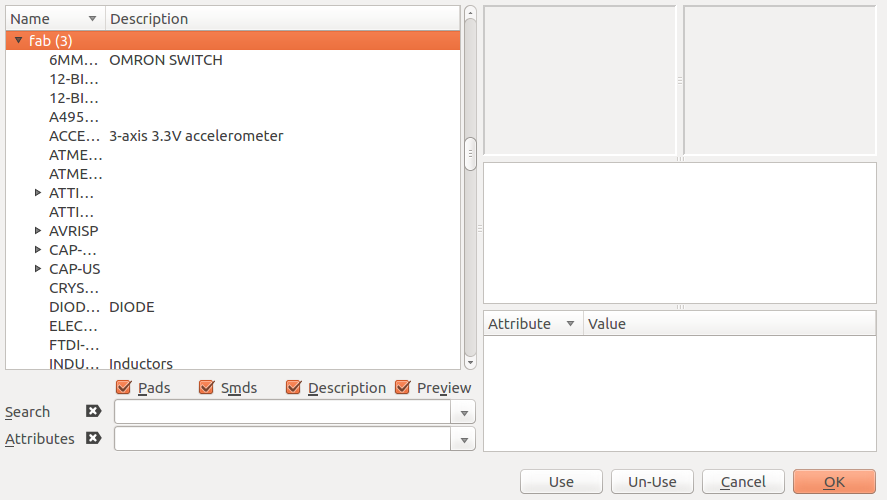
We search for our Fab file by using the search box.
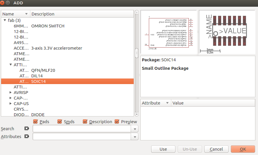
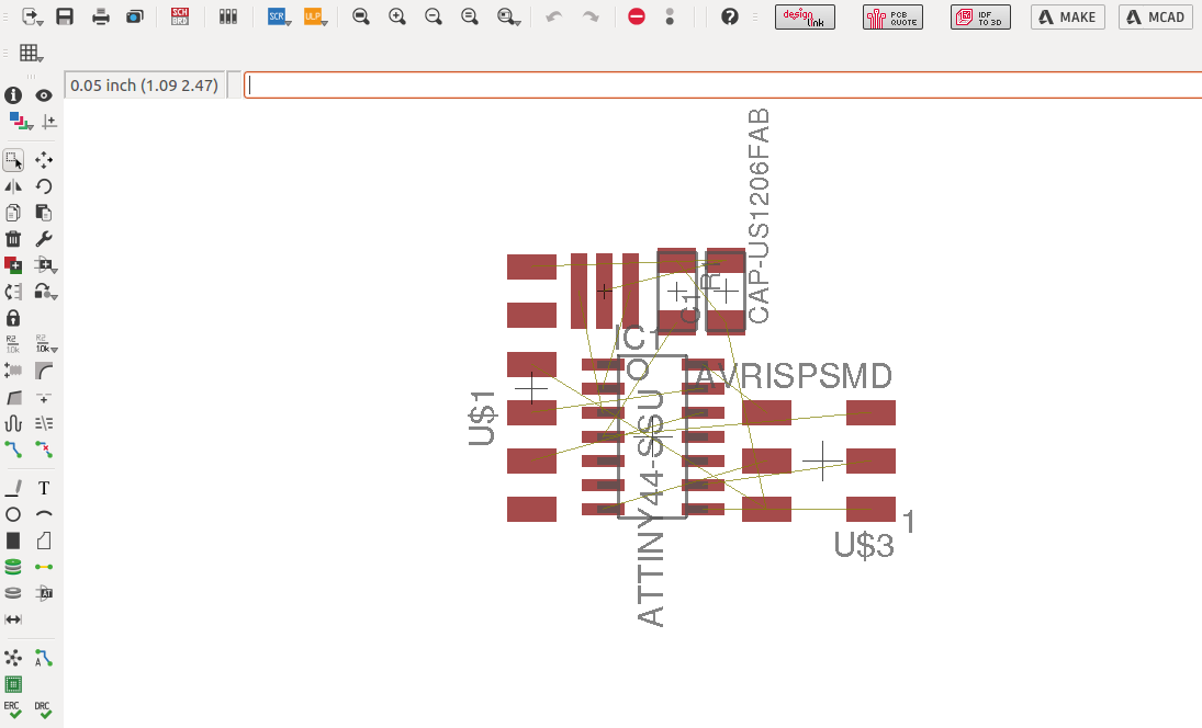
As it shown in the trace map of the board, we need to find the middle part which is the ATTINY44-SSU SOIC14 which is the same shape as on the map.
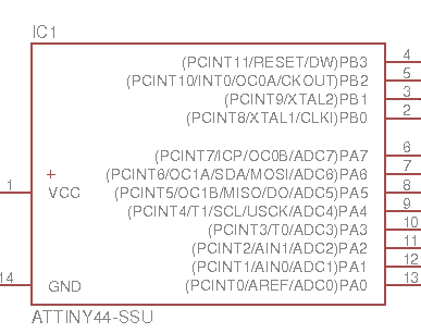
This is the ATTINY44-SSU will be placed in the middle and will be connected with the rest of the components. The other components will be placed arround it too.

To connect the components together, we use this tool called "NET" which is the above. The bottom tool is called "Label" and this will be explained shortly.
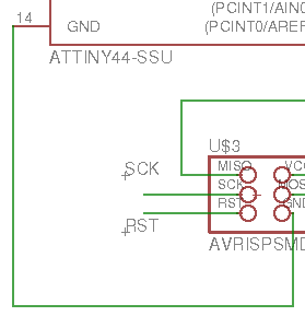
We have connected the Ground "GND" from the AVRISPSMD to the "GND" on the ATTINY. It is shown in the picture that the line connecting both "GNDs" is creating confusion. Imagin the whole components are fulled with NETs like this. It will be chaos.
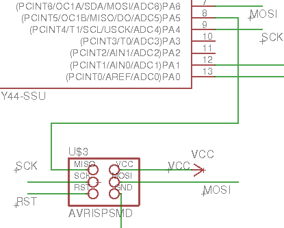
So, the best solution is to use the "Label" tool to make the schematic more clear and organized. To use this tool, need to add a NET on the two components that will be connected and make a small line to both of them. After that click on the "Label" and click on the on of the NET lines to create a Label. Then, Right Click on it and NAME. Use the name of the component for example SCK. Then go on the other NET line and Right Click on it and NAME it to the first component SCK. A message box will appear to agree on the connection, press YES.
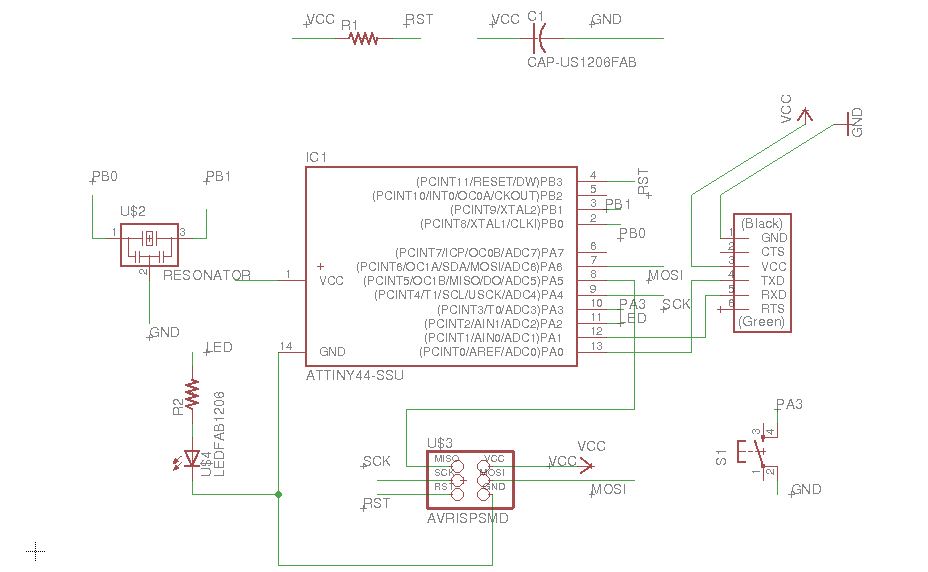
When continue on this process, we will create this board.
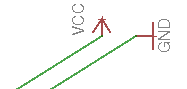
We need to put a symble on the GND and VCC to recognize them.

Now, to test the board schematic, we need to press on the GENERATE tool. This will lead us to the next window.
In this window, we need to gather all the components and test the board using the Autorouter tool.

This is the Autorouter tool
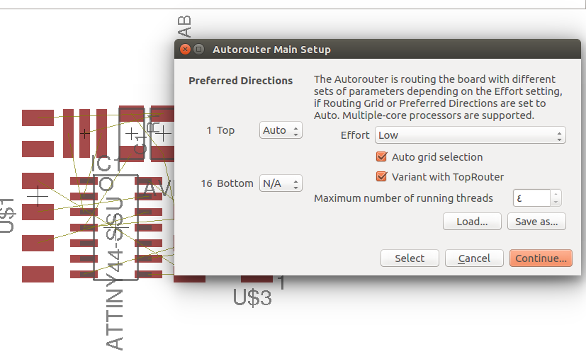
We need to use only Top direction for our board. So we need to tick the Top only and then press continue.
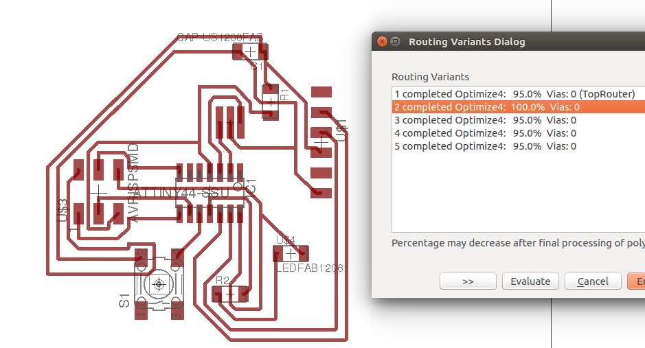
A measurement box will appear indicating the accuracy of the board and effectiveness. At least one of the routs has 100%.
Problem Solving
We need to use the "Label" connection rather than "NET" to avoid the lines on the schematic and reduce chaos.
We need to put a symble on the GND and VCC to recognize them. Otherwise, you will never know which one is the VCC or GND.
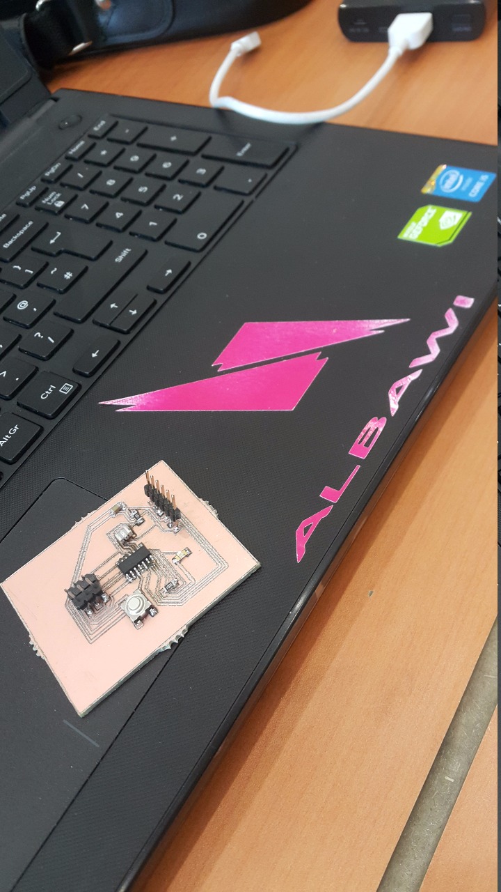
Final Outcome
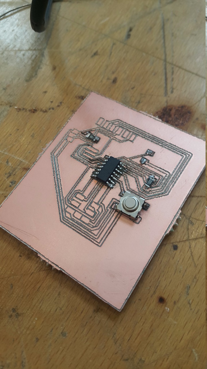
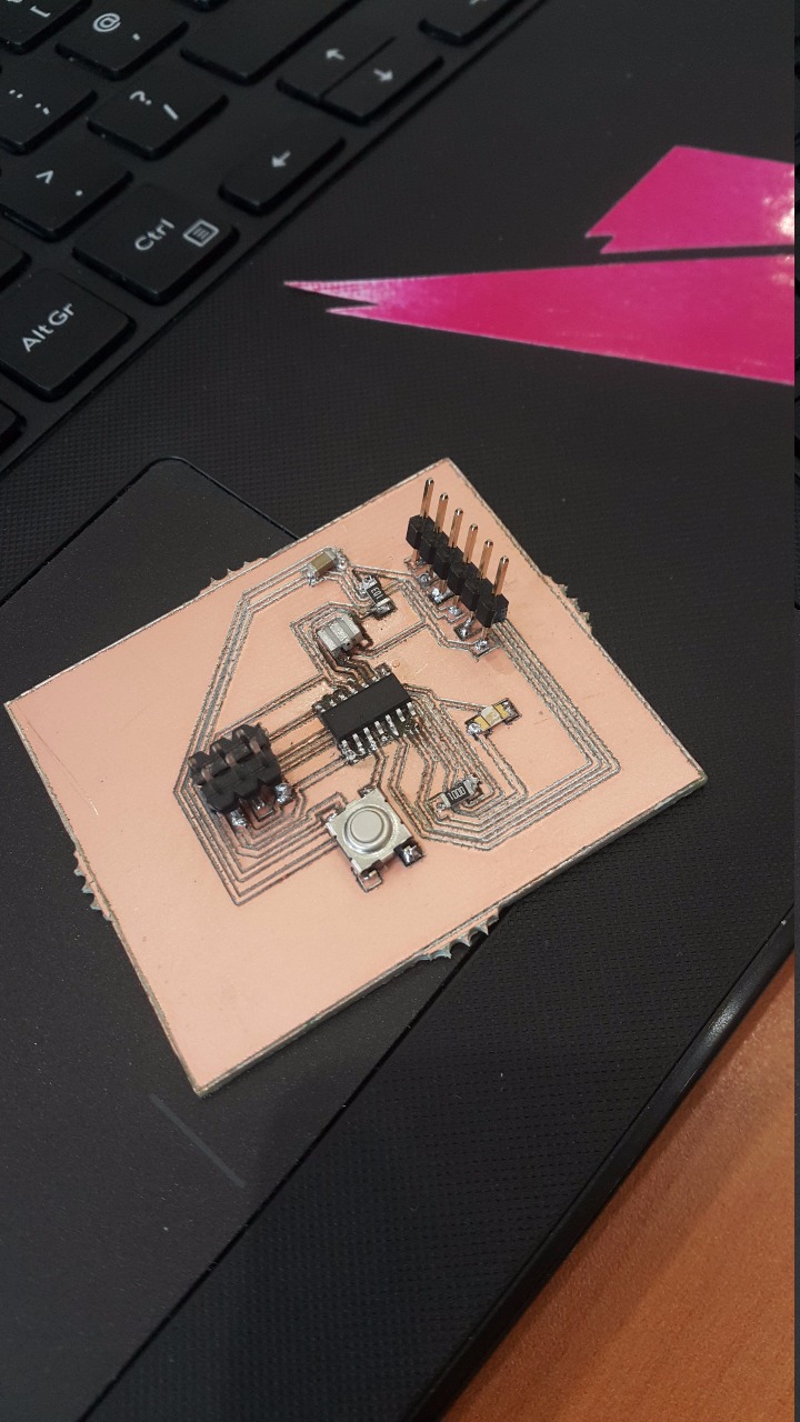
The components used for this PCB
- Attiny 44 - Capacitor 1 UF - Resistor 10 K - FTDI SMD Header - AVR ISP SMD header to program - LED (1) - Resistor 100 ohm - 6mm tact Switch - Resonator 20 mhz
Download Files
Eagle tutorial
This is a very simple guide on how to use the eagle software explained by Jeremy Blum:-