
- This week's lecture : Lecture
- Fab Tutorial Link : Tutorials
- Fab Tool's List : Tools List
Assignments:
- Redraw the echo hello-world board, add (at least) a button and LED (with current-limiting resistor)
- Check the design rules, and make it
extra credit: simulate its operation
extra credit: measure its operation
What I did this week?
- Learned to use software for circuit board design
- Demonstrated workflows used in circuit board design
- Set design rules
- Included original files for download
This week, Prof. Neil taught about various electronic components and electronic designing tools. Our assignment for this week is, to redesign HelloWorld PCB with some extended features, an LED and a push button.
On the first day our instructor Sibu gave a brief introduction to some basic electronic concepts. We discussed about pull-up and pull-down resistors, filter capacitors, Ohm's Law and Kirchoff's Laws. I started with The art of electronics by Horowitz and Hill which is known as The Bible of electronics. I went through some pages so that I can revise some basic concepts in electronics.
Then I went throught a tutorial created by Sibu, Yadu and Vishnu (fab-instruct). It helped really well to get a start with what to do this week. There are some nice tutorials at the end of that page.
Here are some basic concepts in electronics. I hope this would help somebody later.
1.Electronics Fundamentals:
i. Ohm's Law:
Ohms Law states that the current through a conductor between two points is directly proportional to the voltage across the two points. Introducing the constant of proportionality, the resistance (R), relationship can be described as,
V=IR
where I is the current through the conductor in Ampere(A), V is the voltage measured across the conductor Volts(V), and R is the resistance of the conductor in Ohms.
ii.Kirchoffs Current Law:
At any node in an electrical circuit, the sum of currents flowing into that node is equal to the sum of currents flowing out of that node. Or in other words The algebraic sum of currents in a network of conductors meeting at a point is zero.
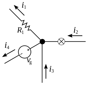
According to KCL i2 + i3 = i1 + i4
iii.Kirchoff's Voltage Law:
Sum of the electrical potential differences (voltage) around any closed network is zero, or More simply, the sum of the emfs in any closed loop is equivalent to the sum of the potential drops in that loop
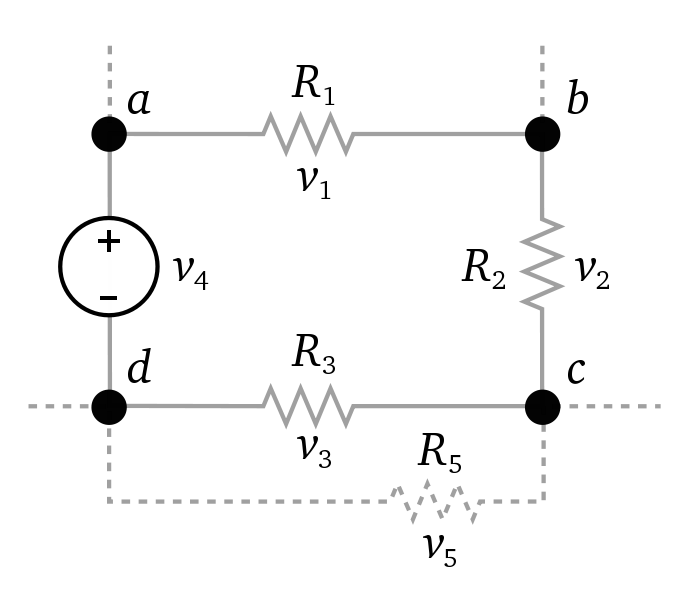
so according to KVL v1 + v2 + v3 - v4 = 0
Pull Up Resistors:
Pullup resistors are resistors used logic circuits to ensure that a wire is pulled to a high logical level in the absence of an input signal. A pull-up resistor pulls the voltage of the signal it is connected to towards its voltage source level. They may also be used at the interface between two different types of logic devices, possibly operating at different logic levels and power supply voltages.
Pull-up resistors are not a special kind of resistors; they are simple fixed-value resistors connected between the voltage supply and the appropriate pin, which results in defining the input or output voltage in the absence of a driving signal.
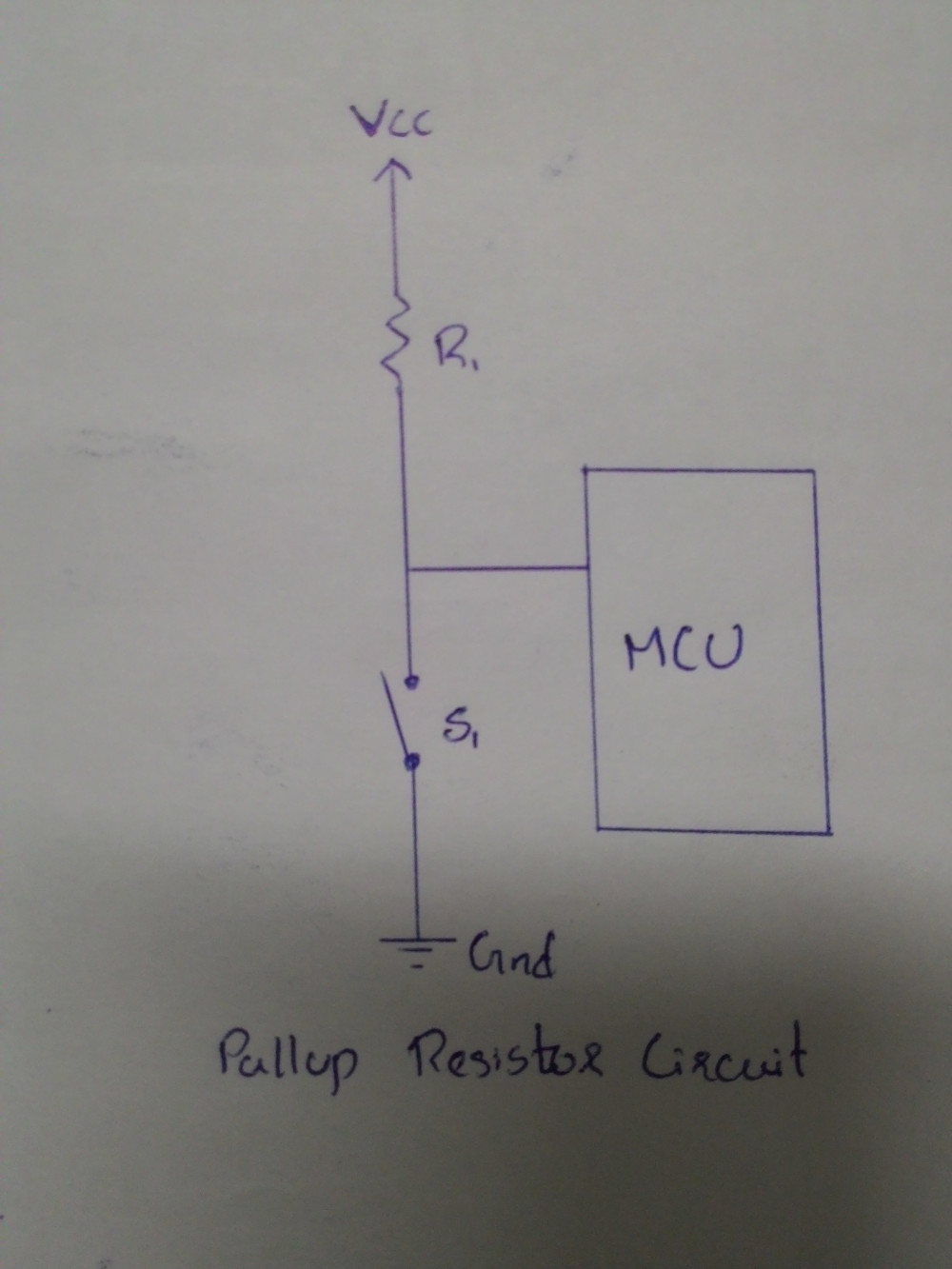
Here when swith is closed, voltage level at MCU pin is low. When the switch on the line is open, it is high-impedance and acts like it is disconnected. Since the other components act as though they are disconnected, the circuit acts as though it is disconnected, and the pull-up resistor brings the wire up to the high logic level.
Pull down resistor
Pulldown resistors work in the same manner as pull-up resistors, except that they pull the pin to a logical low value.
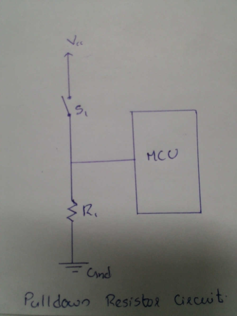
Here when swith is open, voltage level at MCU pin is low. It holds the logic signal near zero volts when no other active device is connected.
Filter capacitor
This article was useful in learning about filter capacitors. Filter capacitors are capacitors used for filtering of undesirable frequencies. Filter capacitors work based on the principle of capacitive reactance. Capacitive reactance is how the impedance (or resistance) of a capacitor changes in regard to the frequency of the signal passing through it. Resistors offer the same resistance to a signal, regardless of the signal's frequency. A capacitor is a reactive device. Its resistance, will vary according to the frequency of the signal passing through. Capacitors are reactive devices which offer higher resistance to lower frequency signals and lower resistance to higher frequency signals.
XC= 1/2*pi*fc.
Crystal
Quartz crystals work by converting electrical signals into mechanical vibrations within the crystal which are affected by the mechanical resonances of the physical crystal and then converted back to the electrical domain affecting the circuits accordingly.
The operation of quartz crystals depends upon the piezo-electric effect. When the piezo-electric effect occurs, an electric charge develops in certain solid materials as a result of an applied mechanical stress. This effect converts a mechanical stress in a crystal to a voltage and vice versa, i.e. a stress can cause a charge to be developed across te material, or placing a charge across the material will cause a stress to be set up.
PCB Designing with KiCad
KiCad is a free software suite for electronic design automation (EDA). It facilitates the design of schematics for electronic circuits and their conversion to PCB designs. Tools exist within the package to create a bill of materials, artwork, Gerber files, and 3D views of the PCB and its components.
I installed KiCad using command below.
sudo apt install kicad
I started with this tutorial. I found the following keyboard shortcuts very useful.
| Display Shortcuts | ? |
| Place Component | a |
| Move Component | m |
| End wire | k |
| Rotate Component | r |
Step 1:Adding Required Fab Libraries
I copied this lib file into the following directory.
/usr/share/kicad/library/
Also copied this mod file into the following directory.
/usr/share/kicad/modules/
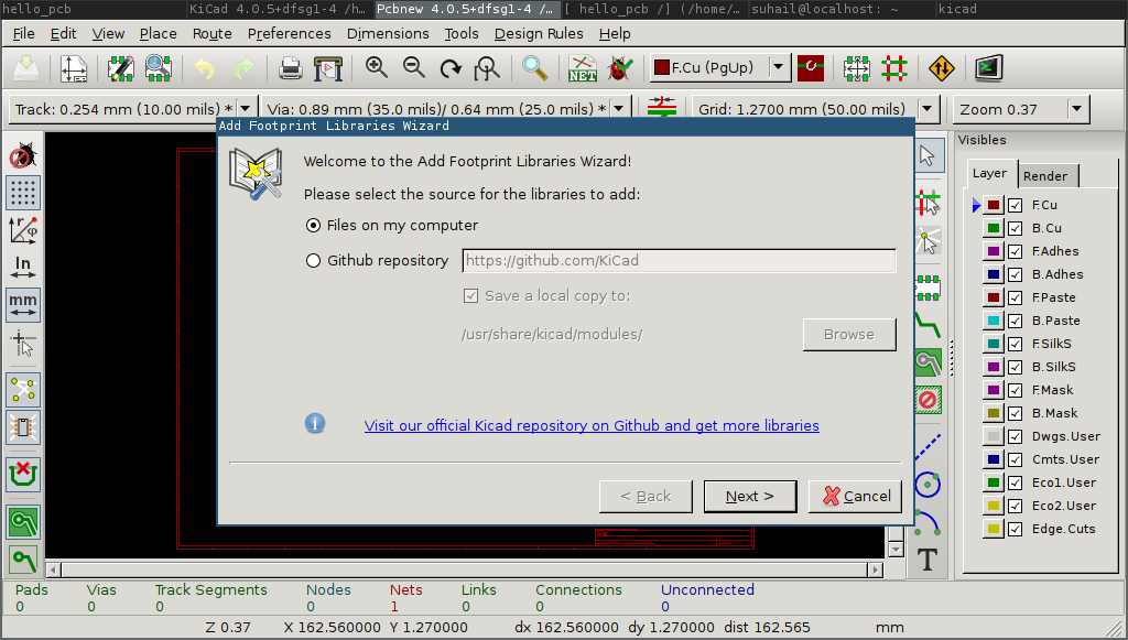
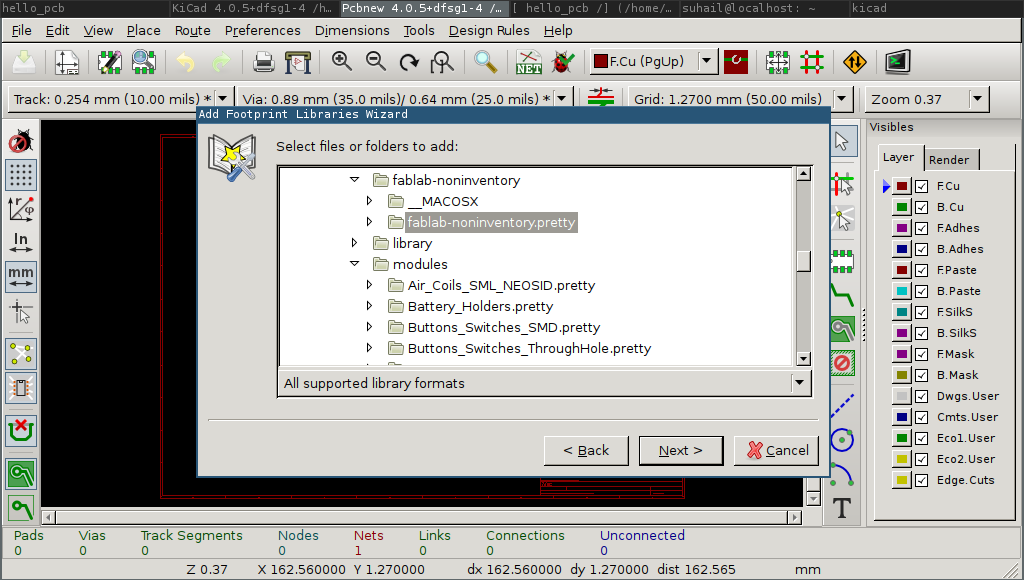
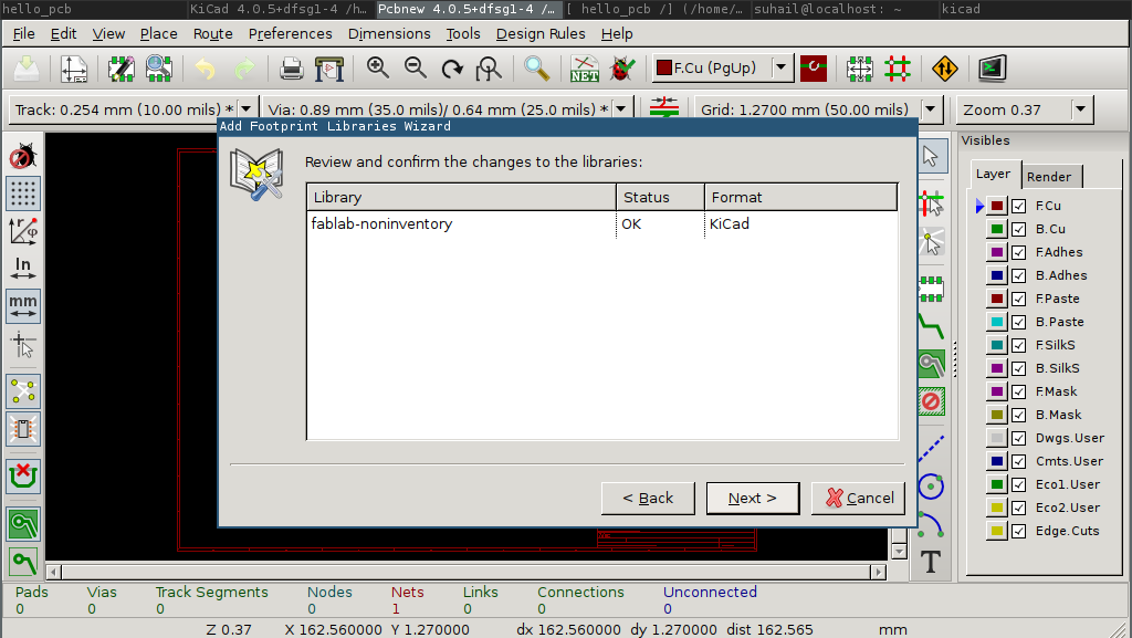
For additional footprints I downloaded this fab-inventory and fab-noninventory files. I extracted the folder and copied to /usr/share/kicad/. Adding these footprints into Kicad is explained in the step 5.
Step 2: Drawing Schematic
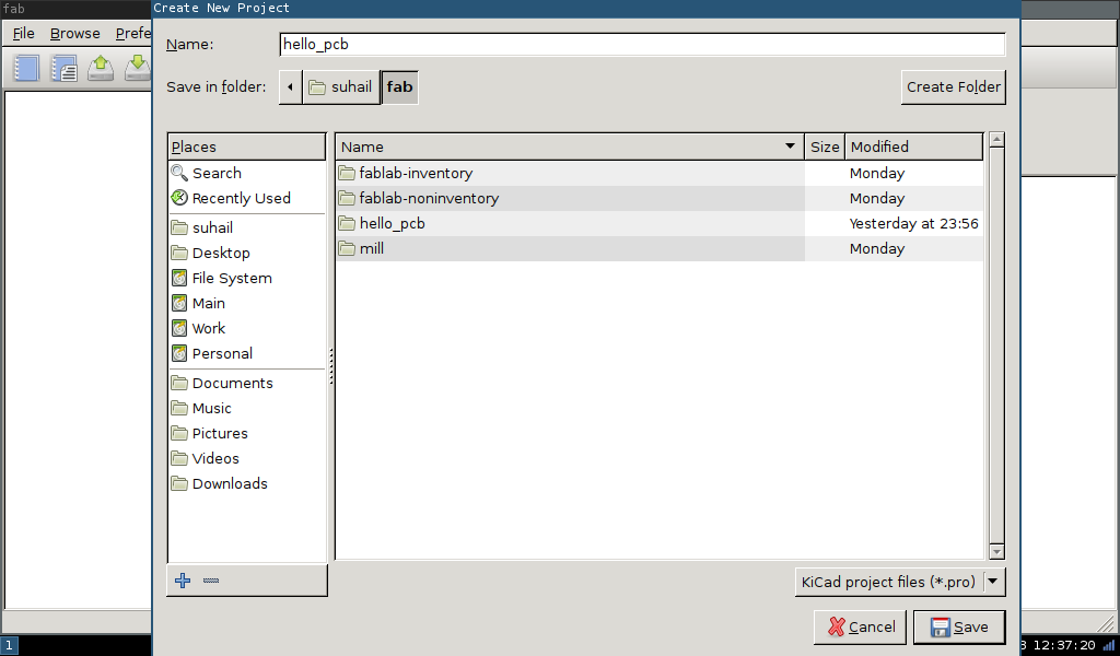
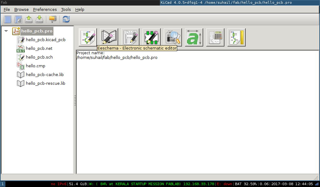
First step is to create a new project. Open Kicad and go to File > New Project > New Project. Choose a project name and save. When KiCad prompts to create a dedicated directory, click "Yes". All the project files will be saved in this directory.
To start creating schematic diagram, use the Eeschema icon which is the first button in tools icons.
To place components press key 'a' and click on any location and choose required components.
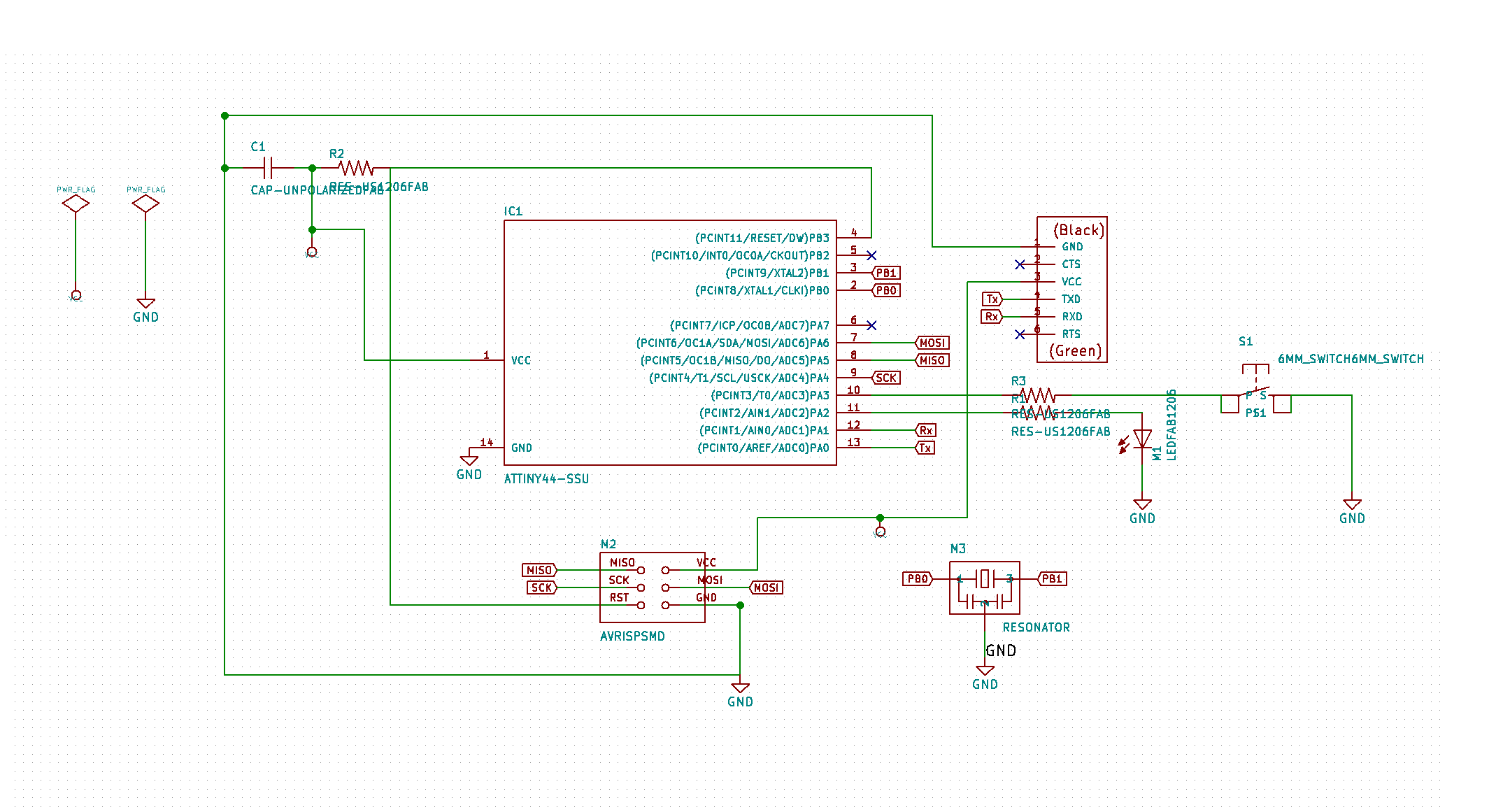
I added the following components
- ATtiny Chip - ATTINY44-SSU
- Resistor - RES-US1206FAB
- Capacitor - CAP-US1206FAB
- Resonator - RESONATOR
- ISP Header - AVRISP
- FTDI Header - FTDI-SMD-HEADER
- LED - LEDFAB1206
- Switch - 6MM_SWITCH6MM_SWITCH
Use place Wire icon from tool bar to connect components. Here is my final drawing.
Step 3: Annotate and ERC Check
For running annotation click on the Annotation button from tool bar. Now Electric rule check can be done using Perform electrical rules check icon which can be seen next to annotation icon.
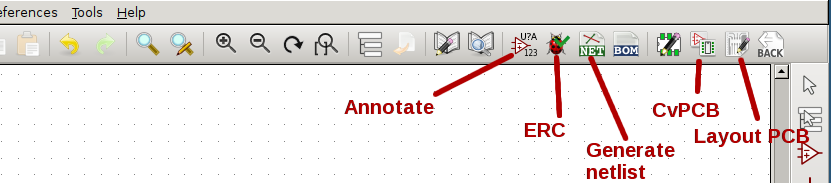
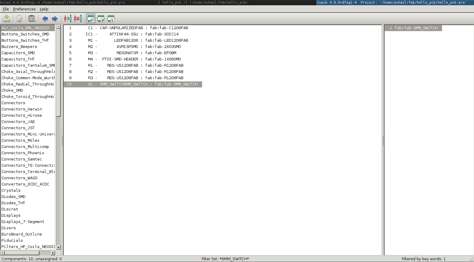
Step 4: Netlist Generation & CvPCB
To generate netlist click on Netlist icon which can be seen next to ERC icon. This would generate list of all components to which we have to add footprints. After generating the Netlist file, click on the Run Cvpcb icon from tool bar. Cvpcb allows you to link all the components in your schematic with footprints in the KiCad library.
Select each item one by one from second panel and choose corresponding footprints from third panel. I selected all components from fab library.
To save Schematic File > Save Whole Schematic Project.
Step 5: PCB Footprints
Click on the Pcbnew icon from toolbar. I added fab-inventory and fab-noninventory modules(I downloaded earlier) using option from Preference > Footprint Libraries Wizard. Below are some sample screenshot.
Now we have to import the netlist file. Click on the Read Netlist icon from toolbar and click on Read Current Netlist from popup window. Then click the Close button.
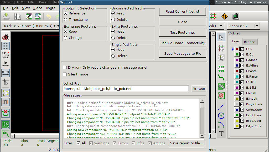
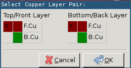
All components should now be visible on the window. I then moved all components to other positions such that wire crossing is minimum. I had made the board single layer. For this use Show active layer section icon from toolbar.
Setting DRC can be done by choosing Design Rules > Design Rules from menu bar. I set clearance & trackwidth as follows.
- Clearance = 0.4
- Track Width = 0.4
Use Add Route tool for drawing routes. For autorouting, click on Mode Track icon from toolbar and right click on the drawing window and then choose,
Autoroute > Autoroute all footprints
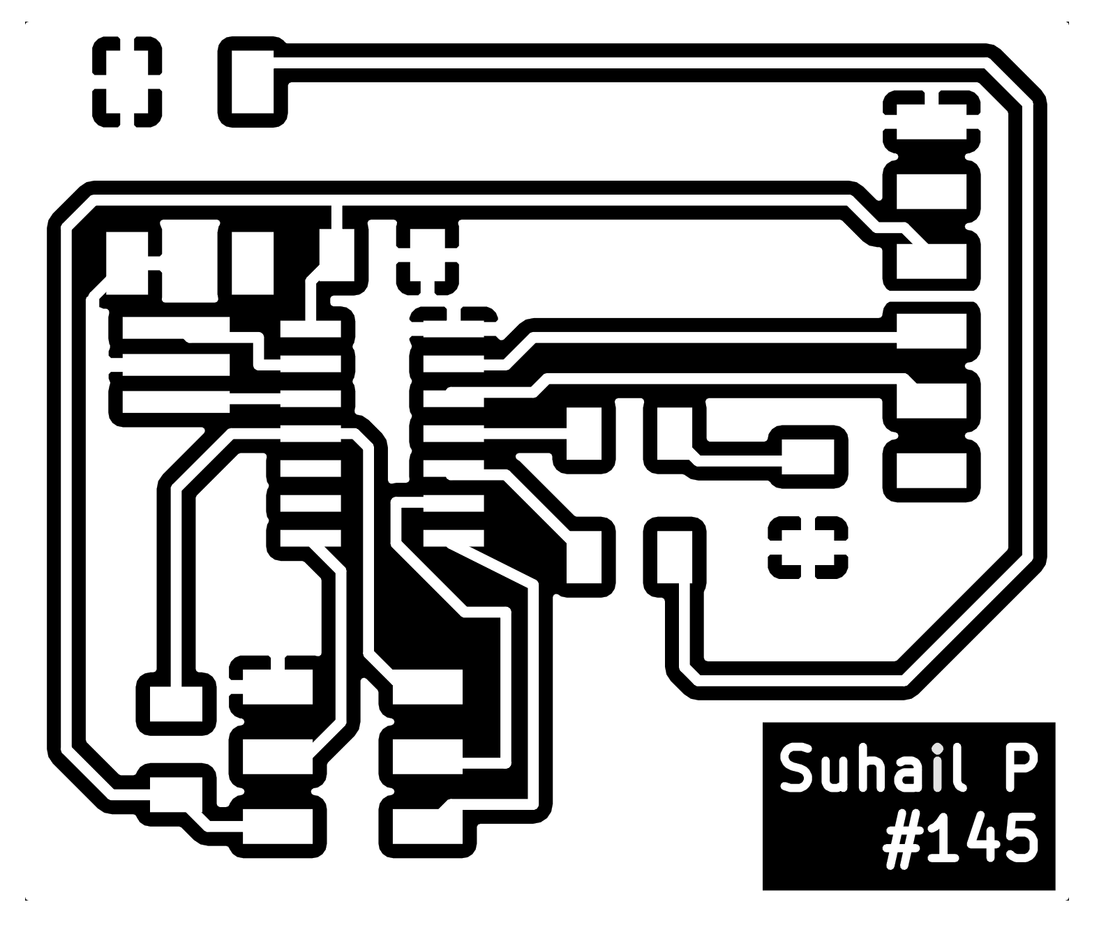
Here is my final footprint image.

Step 6: Exporting to SVG
Select File > Export to SVG, and click on plot. This will create various SVG files. I opened it in inkscape and exported a black & white image with 1000px resolution to PNG format. I created cutout image in required size using Gimp. Below are my trace and cutout images.
PCB trace image
PCB cutout image

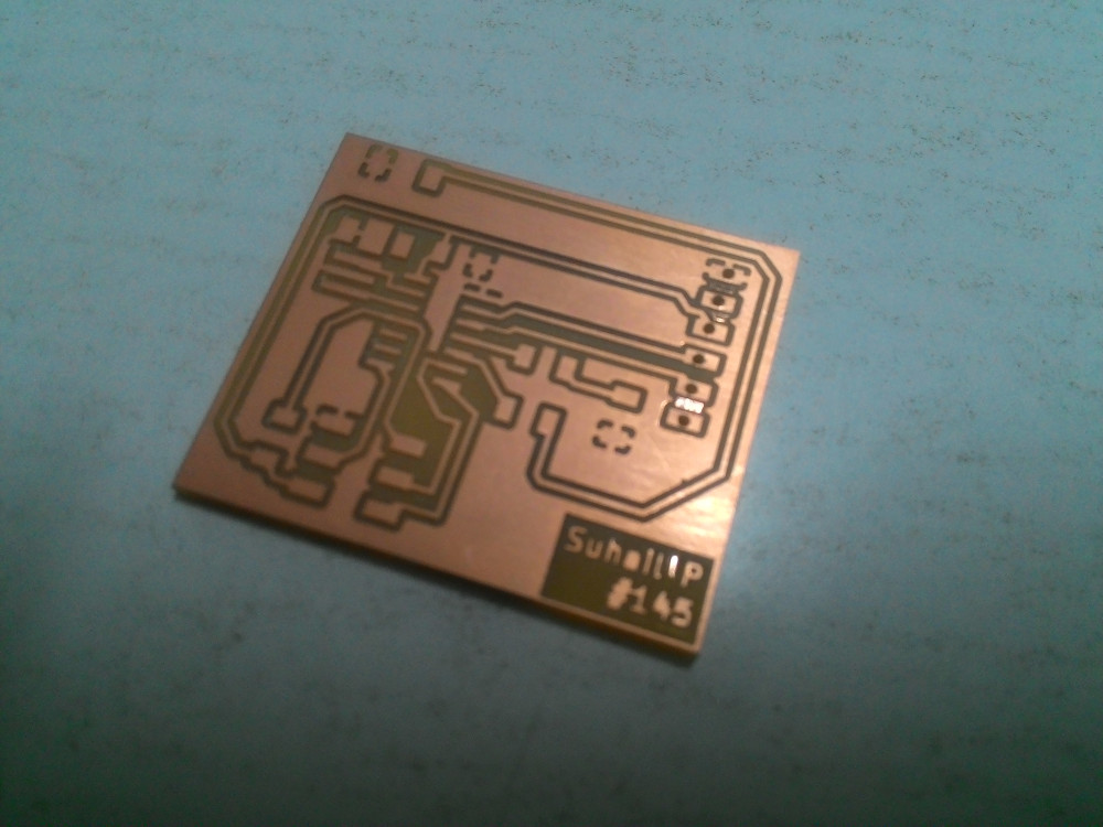
Tracing and cutting PCB
PNG file then fed to modella plotter. Here is my final board
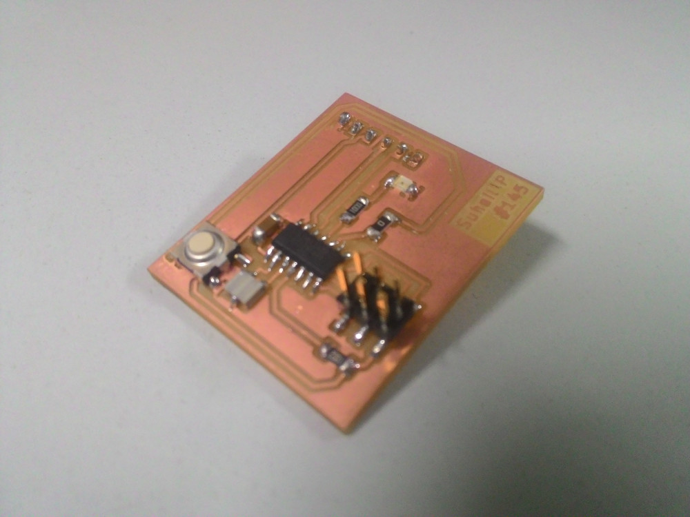
Choosing and Soldering components
To calculate value of resistor to LED I use the following equation. I was using Orange LED (refer digikey.com: 160-1403-1-ND for rating details)
R = (V - VL)/IL
Where V = 5V
VL (LED voltage rating) = 2V
IL (LED current rating) = 20mA
therefore R = 100 Ohm
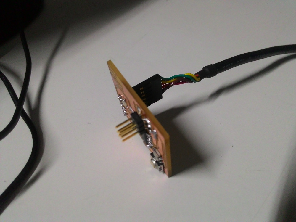
Then I soldered all components and here is the final PCB.
Now its time to check if my fabISP can read this board. For this, I connected this board with fabISP using ribbon cable and connected the ISP into my laptop. To check if ISP can be detected by laptop, I ran the following command.
sudo dmesg
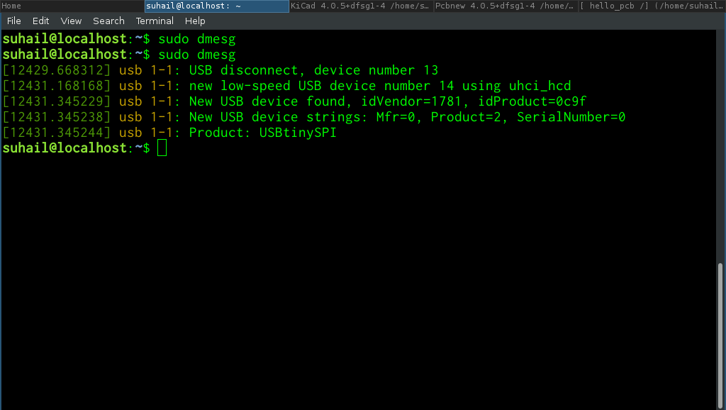
dmesg says it can see the fabISP. Then, I ran the following code to test if ISP can read fuse bits from the new board.
sudo avrdude -c usbtiny -b 9600 -p t44 -v
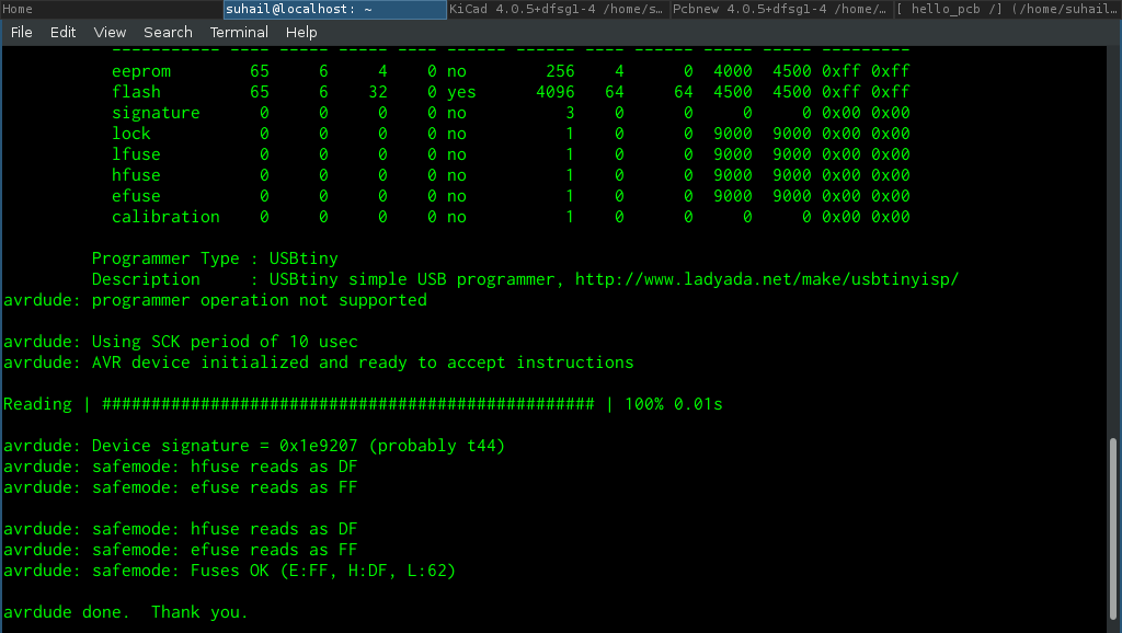
So communication is happening!!! But its not over yet. Its time to check the board by running helloworld program.
Testing the board
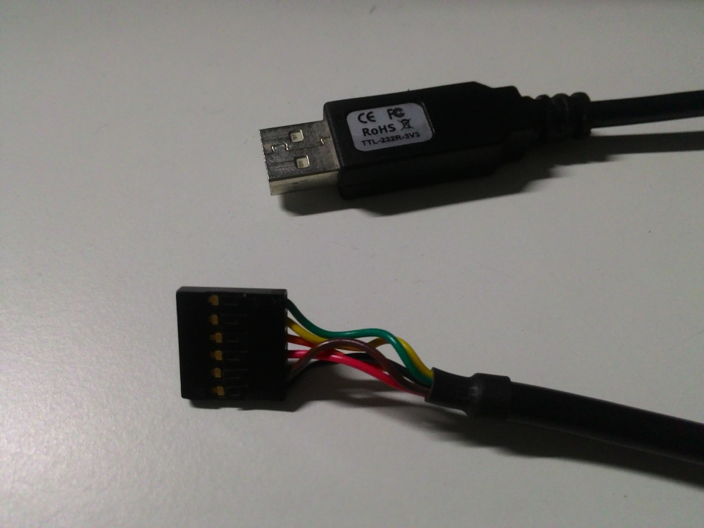
For testing, I have to burn a program into the board and check if serial communication is working using FTDI cable. FTDI cable has one end USB and other end 6-pin female header.
Burning Program
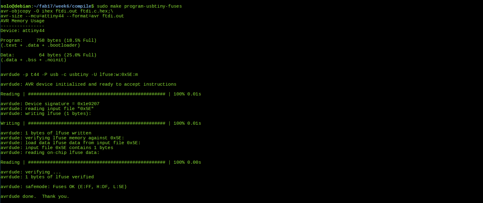
I first downloaded testing program which is available here. Inside the extracted directory, after connecting the board through fabISP into the laptop, I ran the following commands to generate hex file and burn it into the chip.
sudo make program-usbtiny
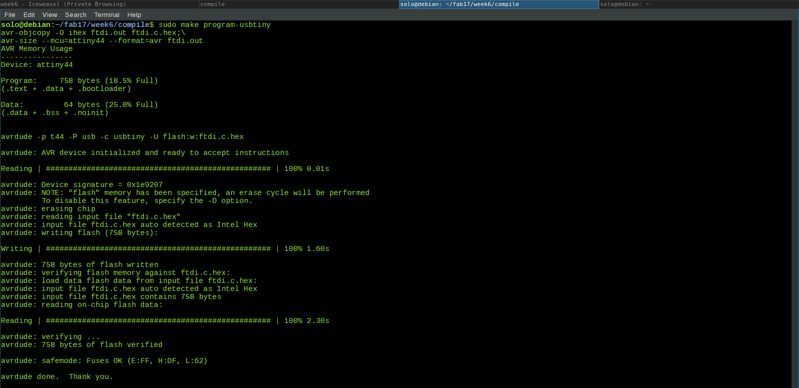
sudo make program-usbtiny-fuses
Now that I have burned the program successfully. Lets move to the final step.
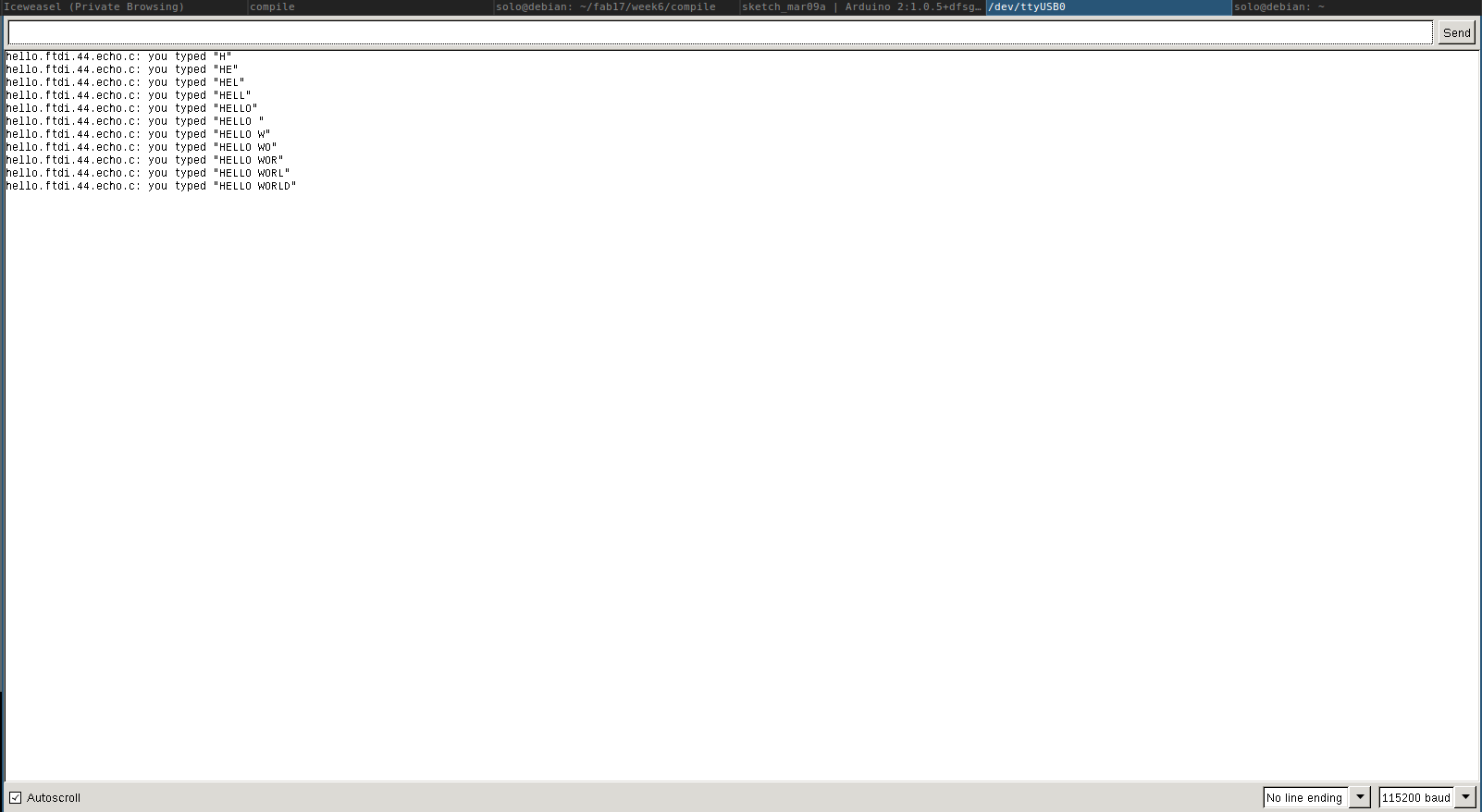
Serial Communication
For this, I connected the board to laptop using FTDI cable.
I used arduino IDE for communication monitoring. I opened arduino and selected Tools > Serial Port > devttyUSB0. Then opened serial communication monitor window through Tools > Serial Monitor. The program I had burned, reads each character one by one and displays it. Note that, I had to choose baud rate 115200 to display the characters exactly.
Problems faced
I struggled a lot to reach the final working state. I spend hours and hours to get the footprints library working, drawing routes and to debug the finished board
1. Issues with footprints : I first used old version of Kicad for drawing schematic and then imported the same schematic into new Kicad. I had imported fab libraries I mentioned in above steps. But there were lots of other footprints missing.
The following are the missing footprints: Buttons_Switches_THT.pretty, Capacitors_THT.pretty, Connectors.pretty, Connectors_mini-universal.pretty, Connectors_Terminal_Blocks.pretty, Connectors_WAGO.pretty, Diodes_THT.pretty, Displays.pretty, Relays_THT.pretty.
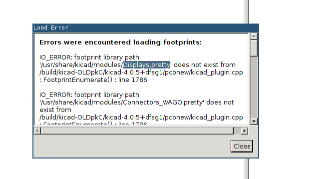
I downloaded all these footprints from Github repository. And copied all directories into KiCad's modules folder.
git clone https://github.com/KiCad/Buttons_Switches_THT.pretty.git
git clone https://github.com/KiCad/Capacitors_THT.pretty.git
git clone https://github.com/KiCad/Connectors.pretty.git
git clone https://github.com/KiCad/Connectors_Mini-Universal.pretty.git
git clone https://github.com/KiCad/Connectors_Terminal_Blocks.pretty.git
git clone https://github.com/KiCad/Connectors_WAGO.pretty.git
git clone https://github.com/KiCad/Diodes_THT.pretty.git
git clone https://github.com/KiCad/Displays.pretty.git
git clone https://github.com/KiCad/Relays_THT.pretty.git
2. ERC Error at pin with no connections: ERC was showing errors at pins which had no connections. To avoid this I had to put No Connect symbol on all unused pins.
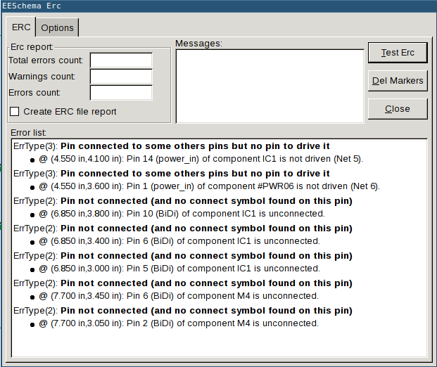
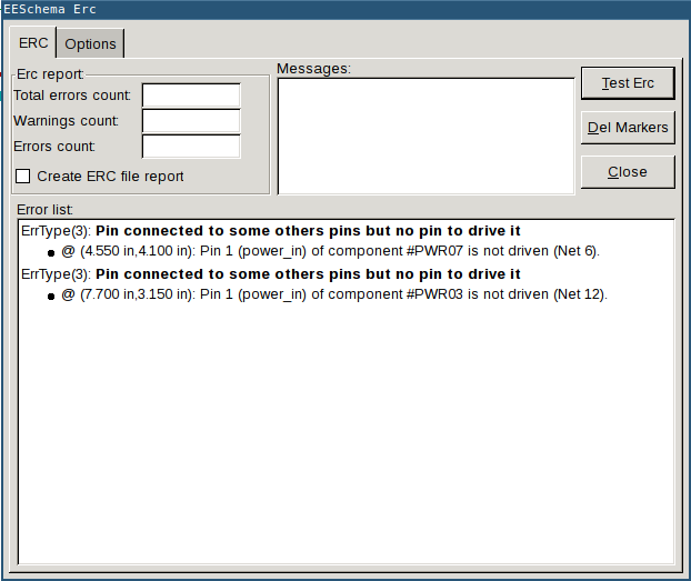
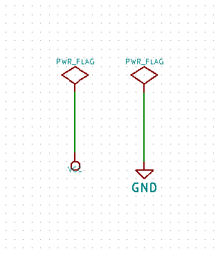
3. ERC error with power source: There was another error in ERC which says that there is no pin to drive the circuit. I had to place extra power flag connected to Vcc and GND.
4. Footprint Routing: As a newbie it was very difficult to route all footprints properly. I spend lots of time doing auto-routing and redrawing again and again. Then I thought manual routing is better. I deleted many routes and drew routes manually. Still there were some routes unable to draw. Then my instructor asked to fill empty spaces as Ground, and connect grounds of components to this common ground space. Everything was easy after that. See my footprint image above.
5. Wrong Positioning of Resistor to switch: I had placed 1K resistor in series with switch and switch is connected to ground. Actually it should act as pullup resistor. When I flashed a simple program to ON the LED, LED was blinking while I place my hand near the board. So, its in floating state. I removed the 1K resistor and short circuited that route with a 0 ohm resistor. And I found, in the datasheet, that IC's internal pullup resistor can be used. Enabling this fixed the issues related to switch