We had the Neil Gershenfeld's on 1st March, on the electronic circuit PCB designing and programming. This was officially my first week to get a lecture on electronics, and got to know about many softwares where I can design the PCB.
Well this week it was much easier for me to do the soldering and milling task, as I already did these tasks in week 4. I successfully created the PCB and learnt how to debug, rules of milling and soldering.
Before going deep in my week tasks, let me give you an overview on the components and their working and usage.
“A microcontroller (or MCU for microcontroller unit) is a small computer on a single integrated circuit. In modern terminology, it is a System on a chip or SoC. A microcontroller contains one or more CPUs (processor cores) along with memory and programmable input/output peripherals.”
ATTINY 44 MicroController
A resistor is a passive two-terminal electrical component that implements electrical resistance as a circuit element. In electronic circuits, resistors are used to reduce current flow, adjust signal levels, to divide voltages, bias active elements, and terminate transmission lines, among other uses.

Resistor
A capacitor is a passive two-terminal electrical component that stores electrical energy in an electric field.
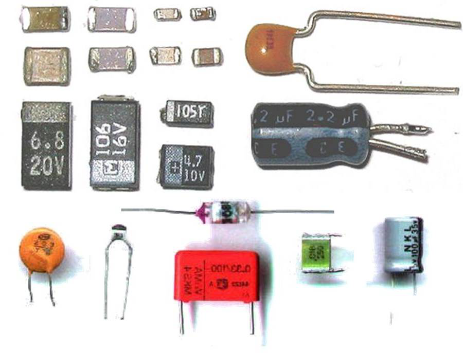
Capacitor
A resonator is a device or system that exhibits resonance or resonant behavior, that is, it naturally oscillates at some frequencies, called its resonant frequencies, with greater amplitude than at others. The oscillations in a resonator can be either electromagnetic or mechanical (including acoustic). Resonators are used to either generate waves of specific frequencies or to select specific frequencies from a signal.
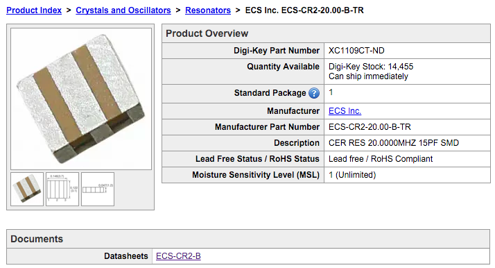
Resonator
Well this was the task, well I sub-divided this task in 4 parts.
To start working on PCB designing I first needed to know about the software in which I have to work, I searched multiple tutorials to get a basic knowledge to design the basic PCB. I watched a few video Tutorials of “Jeremy Blum”, to learn the basics about Eagle.
After getting a basic intro to Eagle, I tried to dive deep and learn by practicing. But before practicing, I had to download and install the Eagle.
Download and Install Eagle First
Then second step was to download the Fab Academy Library to use. You can find the "Fab Academy Library Here"
The third step was after downloading the library, is to add that library into the Eagle by copying "fab.lbr" into the Eagle lbr folder, On windows it can be found inside the Eagle Installation Folder
Adding Fab Library into Eagle
After adding the library, now its time to set the library active and available to use from the Eagle Software, as by default even if you add the library it wont be available to use. Open the Eagle Software, Create any project and open Schematic file. From there click Library Menu button, and click use
Using Fab Library into Eagle
After it was the time to create and design the new PCB design based on the hello ftdi board
Hello PCB Board - The PCB board we were provided with
Now its time to start working on PCB Designing, I started by creating the new empty project and trying to copy the exact same design as the Hello FDPI board, as a practice and also so that I can improve it later. After a few fail attempts, adding and removing components I finally completed the schematic design of the wanted PCB Board. I added one more component than the asked assignment, as I wanted to make some thing useful in future as well.
My Modified Schematic
My Modified Board Design
After making the Board file, I exported board file to PNG image file, and opened that with Photoshop so that I can create a Outline File. I learned this trick from our Instructor to make outline using Photoshop.
I opened the file in Photoshop as it was in Indexed Color Mode and layer locked, firstly I have to go in the Image menu, then to Mode and change Mode to RGB, and then Unlock the layer.
Then increase the canvas size by 1 or 2 millimeter, which will be our Outline File, by going in Image Menu and to canvas size.
Then create new layer, and by using magic tool select the transparent area from our traces layer and without deselecting go to layer 2 and color this area black.
then coming back to our traces layer color this area black as well. And thats done we created 2 layers, one our Traces and other Outline
Creating Outline Using Photoshop
Outline Using Photoshop
My PCB Traces
My PCB Outline
Resources available for Download and Re-use
The next task after the PCB designing was to mill according to your PCB, well its not a difficult job if everything goes smooth as I don't have to do anything practically but to generate the code file for the Milling Machine to mill the PCB for me.
There are just a few things for focus here, the PCB board is straight, and the X, Y, Z position are set perfectly for the board to be Milled, and after the traces are done then replace the 1/64 (used for traces only) head with 1/32 (used for outline only) head and change the file relatively to start.
Converting my .PNG traces image to Roland SRM 20 Machine understandable code.
Converting my .PNG Outline image to Roland SRM 20 Machine understandable code.
Once the Code is generated, its practically just sitting before the machine and overlooking the process is going smoothly.
Milling Process
Milling Completed, and the desired PCB is developed
Resources available for Download and Re-use
After the Milling task is completed, now its time to start the most difficult task of this process, that is soldering. Well as I already had done soldering before, now it was much easier and I done much better work then previous.
First task first, make the list of components needed and picking them up accordingly
Components list needed to Solder the PCB
This process though tough, but is too interesting and intriguing, as I forgot to do lunch and kept working on soldering different components until I finished the soldering work
Soldering Components
Completed PCB
Now this part was quite interesting, to find out what components are working perfectly and what not, I used Digital Multimeter to check the various inputs and outputs of the attached components, and I found that unfortunately my circuit wasn't working perfectly. The Resonator was not working perfectly (and it was really hard to solder as well). It was getting input but not giving output ... I might have not soldered it properly. So I desoldered it with the "Desolder Gun" and re-attached the Resonator
Checking the board
After desoldering it, I rechecked my whole PCB to find the issues, and this time I didn't found any issue after repeatedly testing the each and every component multiple times.