
Assignment
- redraw the echo hello-world board and:
- add (at least) a button and LED (with current-limiting resistor)
- check the design rules, and make it
1. Redraw the echo hellow-world board
The first think in this week that we need to do is to get fimilare with EAGLE (Easily Applicable Graphical Layout Editor). Becasue we can easily redraw the required cirucit in this software as well as pcb board can be easy generated in it.
EAGLE can be downloaded from here
After the installation of the EAGLE the next target is to get fimilare with. Here is the very easy and usefull tutorial from which we can learn how to draw the circuit diagram in this software.
The Next very important thing is to include fab library to the eagle. It is really important because the component that we use to draw any circuit must be avalible in our fablab. In this regard fab library help us to give easy path to include component with proper pcb layout.
Here is the eagle library to download
For me the easy way to include the library is to paste the library file into C:\EAGLE\lbr. This will work if you have installed EAGLE at its default location. Otherwise simply go the directory where you have installed the EAGLE and find the "lbr" subdirectory, and paste the "fab.lbr" file there.
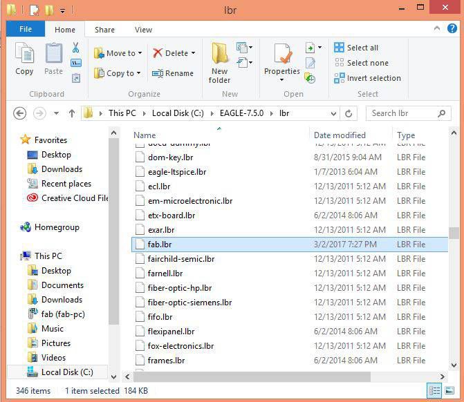
So finally fab library is installed. Here is the snapshot on the library from here we can add components to redraw our hello-world board.
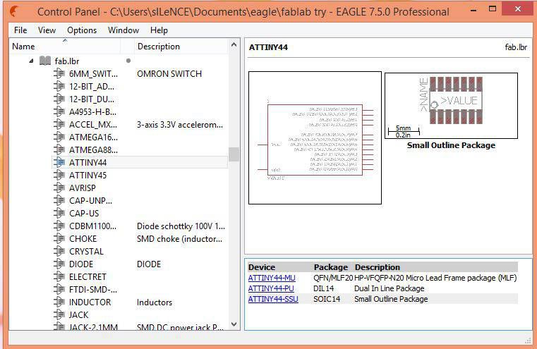
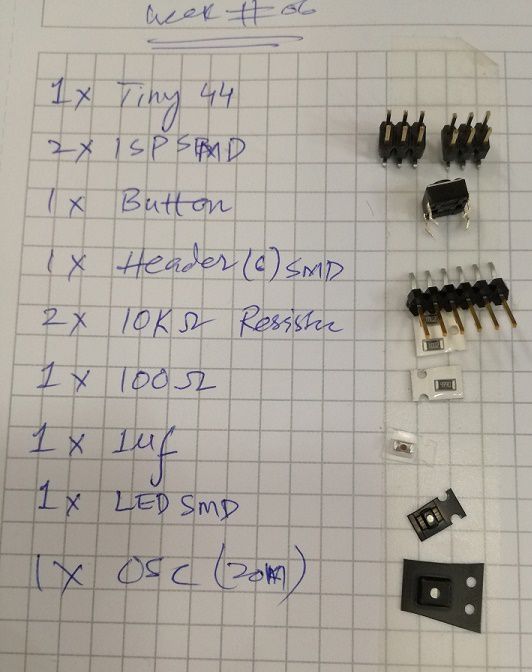
Here is the list of component that we need from this library
- 1x Attiny 44
- 1x capacitor 1µf
- 2x ISP SMD header
- 1x resistor 100Ω
- 2x resistor 10KΩ
- 1x 1x6 Pins SMD header
- 1x LED SMD
- 1x Push Button SMD
- 1x Resonator 20MHz
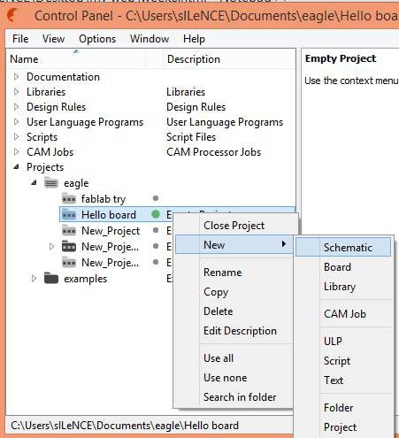
After creating the project we add new schematic in the project
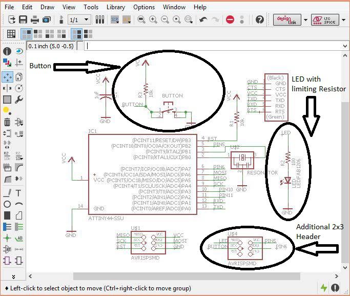
Now its turn to draw the schematic of hello-world board with led and a button. Along with LED and a Button I have also added a 2x3 SMD header and connected LED and Button through this header. This is because in future I will be able to use the IOs of tiny44 to connect any other input/output device with it. Here is my schematic diagram.
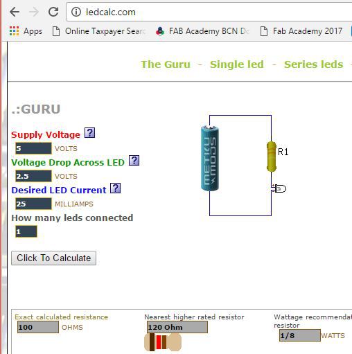
Lets verify the value of current-limiting resistance for LED. LED will be simply connected in series with supply and resistance. we can calculate it by volate divider rule as well. lets go through an online led protection resistor calculator.
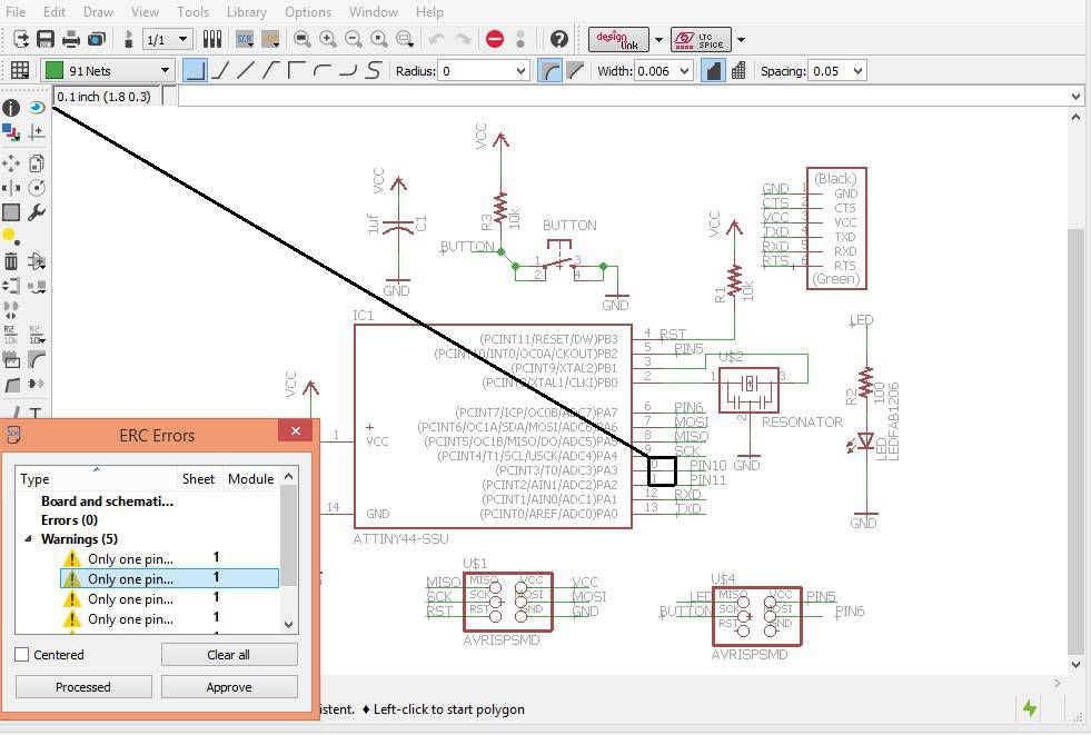
When the schematic diagram is complete we need to check the ERC (Electrical rule check), we can do this by using erc command. In my case I got zero errors and 5 warnings. All warnings are due to unused pins in the circuit. This step is shown here in the image given below
Now the next step to switch to the pcb board, we can switch to the board by click the "Generate/switch to board" icon.
As per my observation there are number of things that we need to take in our consideration while working with Board.
- First thing is to make PCB board as smaller as you can but take care of traces and component, they must not be to much close.
- Second, Move the components at your desired place but make sure that you will be able to find the trace to make the connection, otherwise we need to move to another layer. Which will become difficult and expansive to implement.
- Third, wire width. It is also important, try to make wider trackes for low electrical resistance but the board size will not allow us to do so. So we need to make a trade-off. Make the wire wider where possible and reduce otherwise. In my case I used two size of wire width 0.3mm and 0.4mm
- Open image
- Create a new layer
- Increase canvas size by one mm of new layer and fill back colour in it.
- copy the layer of original image.
- Now hide the original layer an save the image.
- Input the PNG file
- Select your machine, in my case it is roland SRM-20.
- Now Select the tool size i.e 1/64 in case of trace and 1/32 in case of cutting.
- Select the proper tool (i.e 1/64 for traces and 1/32 for cutting)
- Set the origin of machine and save it.
- While setting the origin of machine, special care required for Z axis.
After taking into account all the above consideration, finally I have complete my PCB layout ready of hello-world board.

Now the next step is to check DRC (Design rule check) by using "drc" command. A menu will appare in with multiple taps, but we need to go to the clearnce tap and need to put the 16mil in all the fields (as shown in figure given below) it is due to tool size of our milling machine SRM-20.
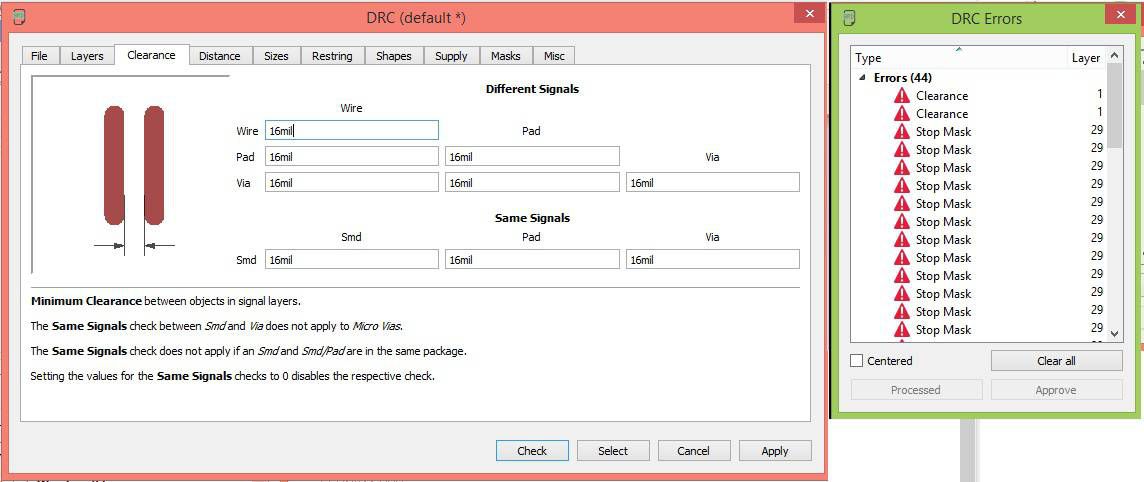
After my first DRC check I got lots of erros (44 erros) because I did a mistake, remember before doing DRC we need to deactivate all the layers on which we are not working. we can do it by clicking at the layer icon given in the toolbar.
Here is the response I got after applying DRC second time, after deactivating all layer which do not need at the moment.
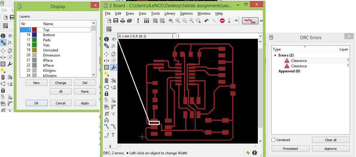
We can see from above snapshot that these two errors are because of line width, so I will reduce the line width to 0.3mm on line segment where I am getting errors.
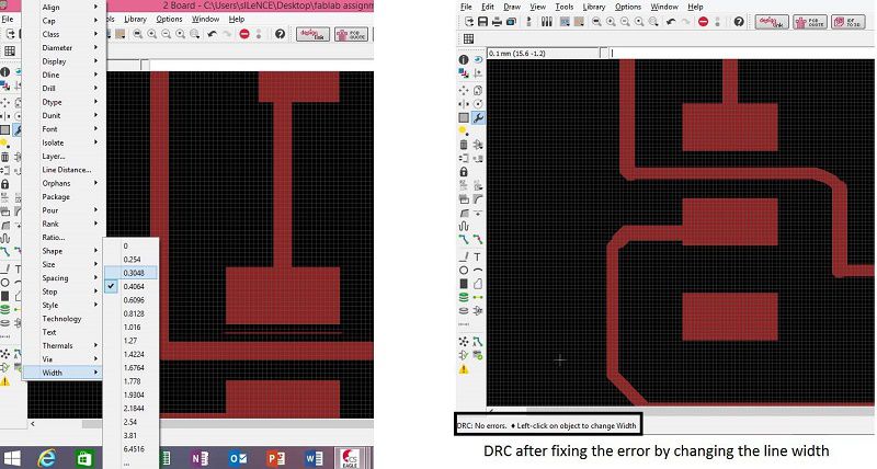
Finally my PCB layout is ready with no erros.
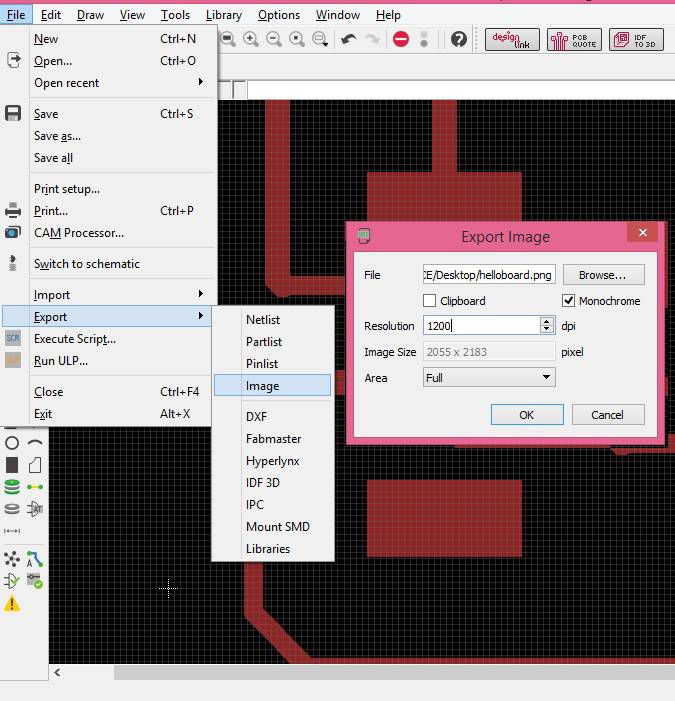
The next step to export the pcb layout to save in as PNG image. we can do it by going to file menu and then export.
Remember we need to save it as monochromatic image. Details are shown in the image given below.
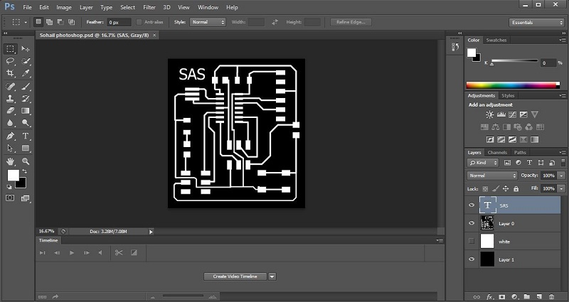
After exporting PNG our PCB layout is ready, Now we need to create its Board that will be used for milling machine to cut the required pcb from copper board. We can do this in Adobe Photoshop.
To create border image in photo shop we need to follow the following steps.
For more details download the photoshop file attached at the end of this page.
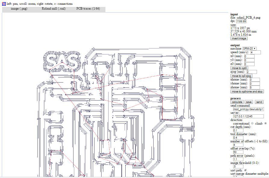
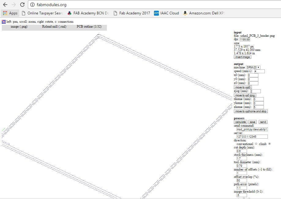
RML files using fabmodules.
To generate RML files for our milling machine Rolland SRM-20 we use the fabmodules.org.
Following are the steps to generate RML using fabmodules.org.
Following images are showing this process and important details
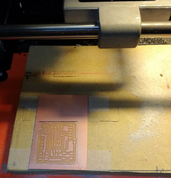
Milling.
Following points shows few important things in milling process.
Remaining process is the same as we have done in Week 4 (Electronics Production)
Soldering.
Again the same process of soldering was repeated as we have done in week 4 to populate our newly developed PCB.
Here is the list of components that we need to implement the circuit.
During initial debuding using DMM(Digital multimeter) I found two pins (2,3) of tiny44 was connected to each other which was not desired, than I isolated those pins. Another thing which I realized during debuding process was that 100ohm protection resistor for LED is not enough I need to increase its value, as 100 ohm was the minimum value that I need to connect, then I replaced it with 499 ohm.
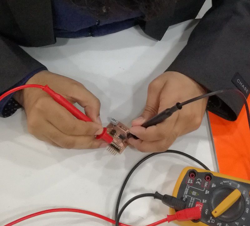
Finally here is my redesigned hello-world board with an LED, button and with an extra 2x3 SMD Header to you free pins to microcontroller for future use. And the circuit is working now. :)

Download All file of this week Here (including RML,PNG and photoshop files)

This work is licensed under a Creative Commons Attribution-NonCommercial-ShareAlike 4.0 International License
.