Electronics Production
Week 4: Assignment
This week assignment is to create an in-circuit programmer using the Milling Machine to create the board, stuff the board and then program the in-circuit programmer to create a FabTinyISP (In System Programmer).
After looking over all the designs mentioned on the archive of "Fab Academy 2017" of the in-circuit programmers, I decided to make Brian's Board and reason I decided upon this because it was an updated programmer. But, It was not getting programmed, I don't know because of what reasons. I have discussed about this in detail below. Since, Brain's ISP didn't worked for me so I decided to make Neil's ISP, which worked fined.
Details and files for Brain's FabISP can be found at "http://fab.cba.mit.edu/classes/863.16/doc/projects/ftsmin/index.html".
I followed the very detailed instructions on the FabTiny ISP page from the Brain link on the archive of Fab Academy 2017.
PCB Fabrication
Milling and Cutting the PCB
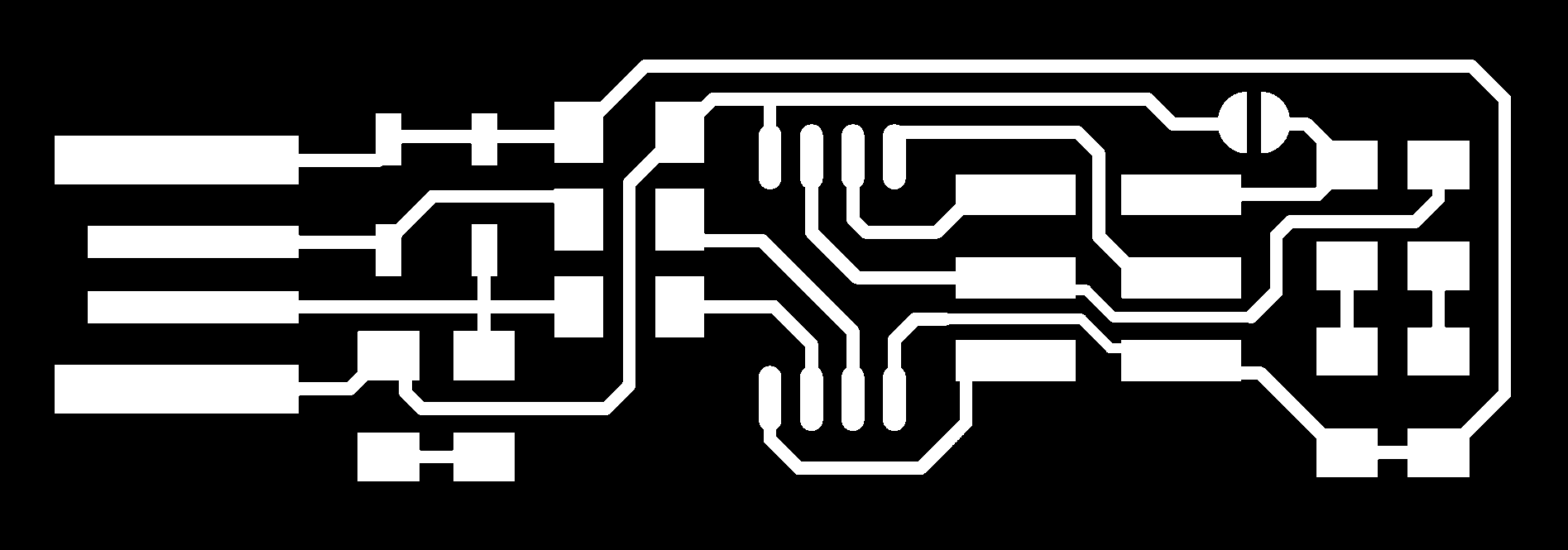
There are n numbers of PCBs available in the market and each PCB is recommended for various specific applications. Some of the commonly used grades of PCB used are FR-1, FR-2, FR-3 and FR-4. I used FR-1 board for milling and downloaded the PNG files for the traces and the board outline as shown below from Brain's link.
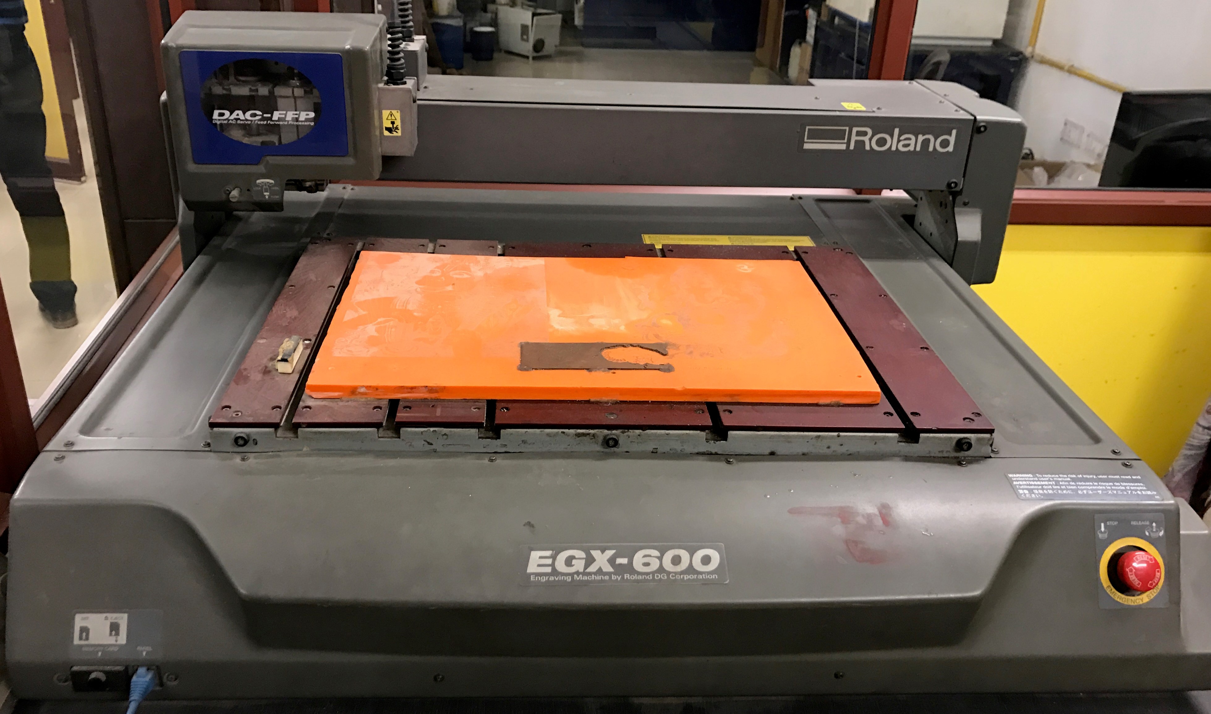
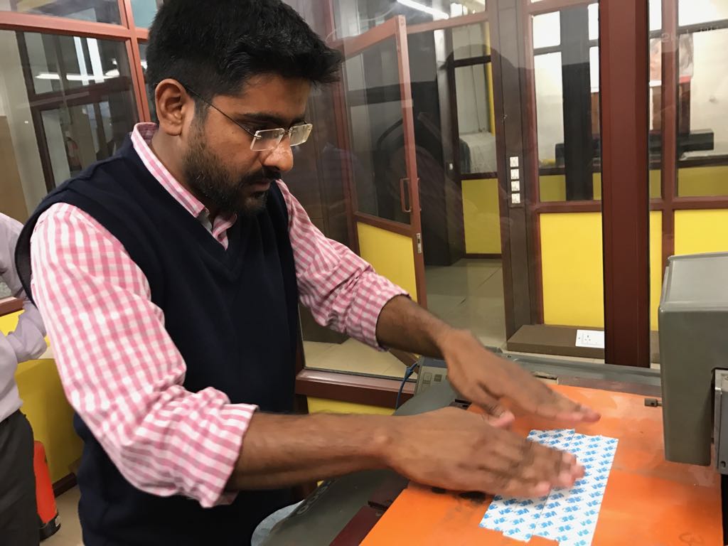
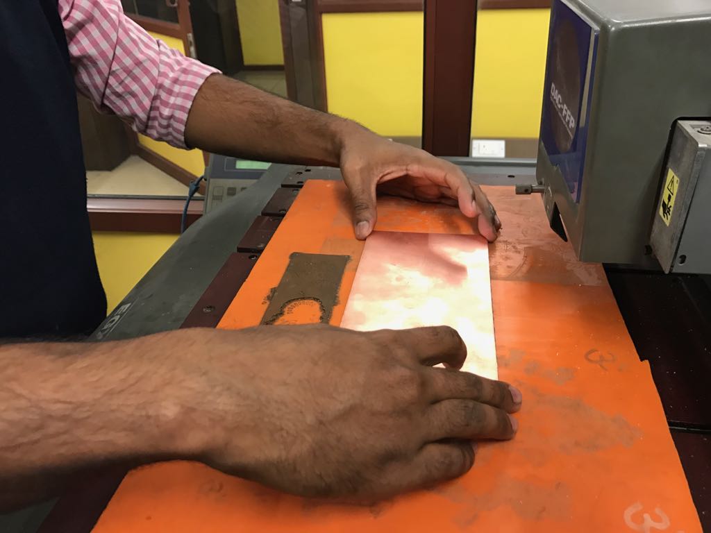
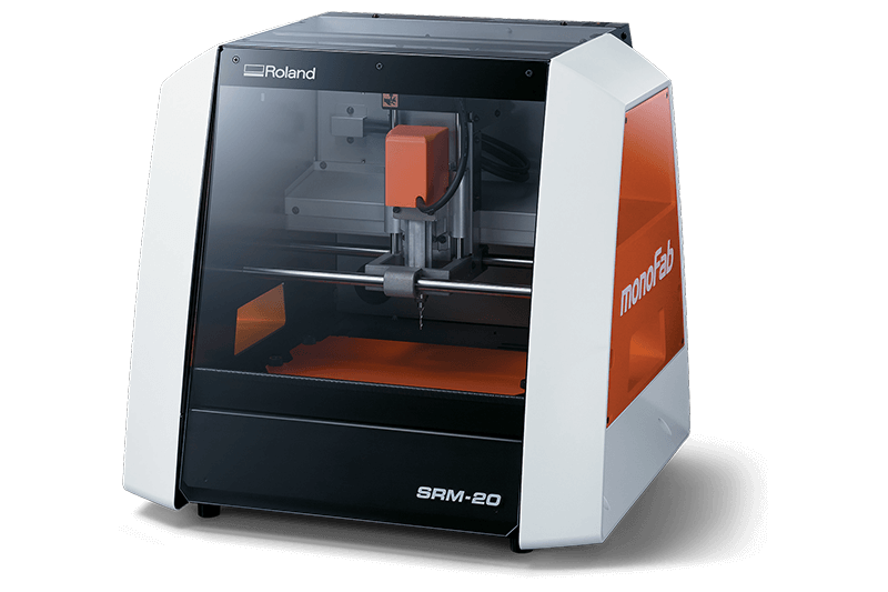
 The Roland EXG 600 Mill was used to trace and cut out the board (As shown below). To start we needed to affix the board to the machine with double side tape and set the origin. This can be seen in the photo below of the EXG 600 getting ready to cut the F1 board out.
 Inkscape is used to trace the png image of the trace and cut and saved it as epc, which is exported to Aspire to trace the path. After milling the traces and cutting the board from it's outline, I found that, the ISP is not fitting inside the USB port because the dimension of the connecting side, which was provided in brian's png image was 12.9 mm and required dimesnions were 11.2 mm (found it after measuring with vernier calliper physically). This was the first PCB milled by me (as shown below).
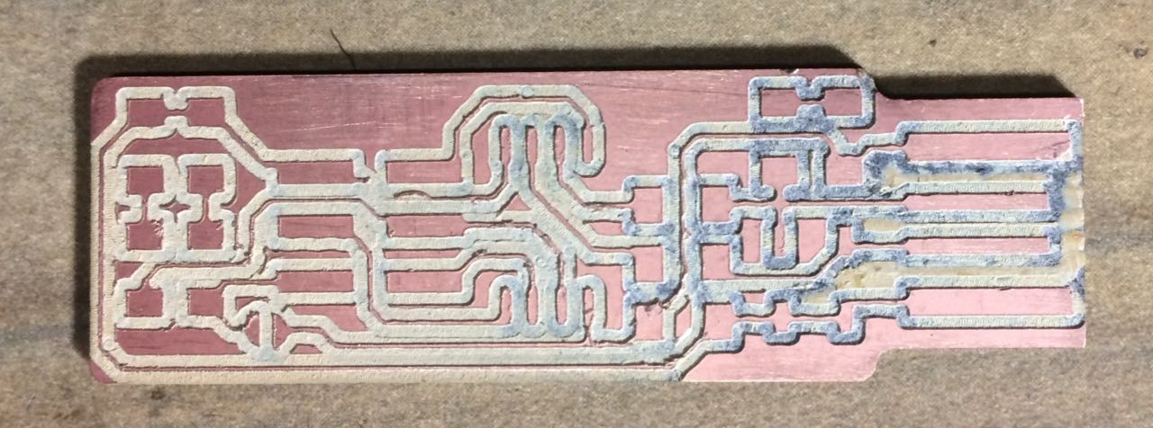
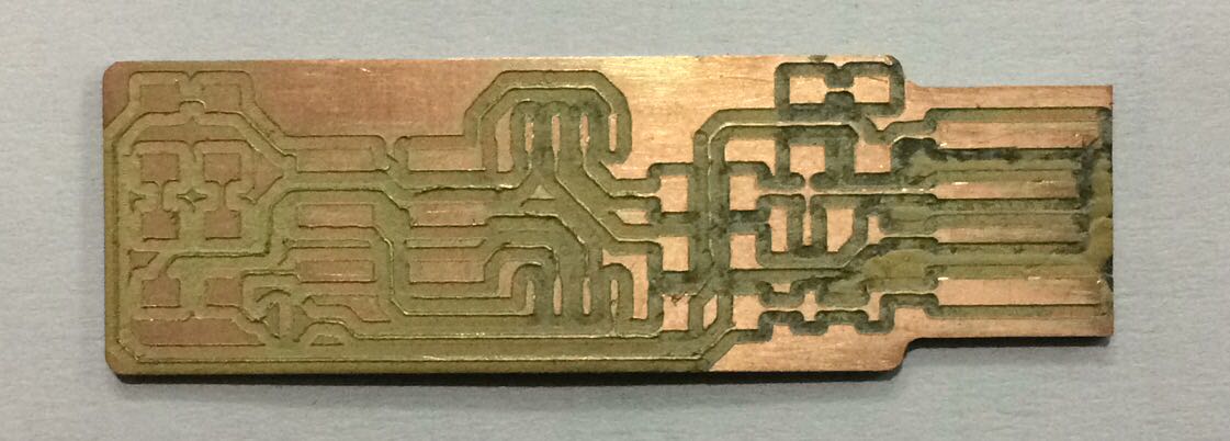 The difference between the available dimension and required dimension was 1.7 mm (12.9 mm - 11.2 mm). So, while defining the cutting parameters in ASPIRE (software to trace the path of the PCB), I reduced the tool dia. from 2 mm to 1.3 mm (But, the actual dia. of the tool used was 2mm),this was done to get offset. Therefore, the PCB obtained after doing all this manipulations is shown below.
Setting the cutting Parameters in Aspire
- esp image is imported to ASPIRE as shown below.
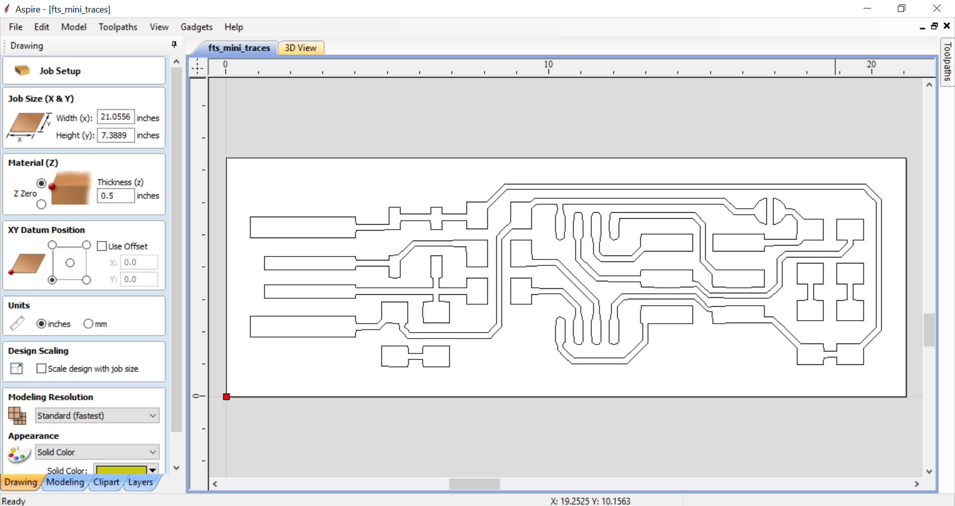
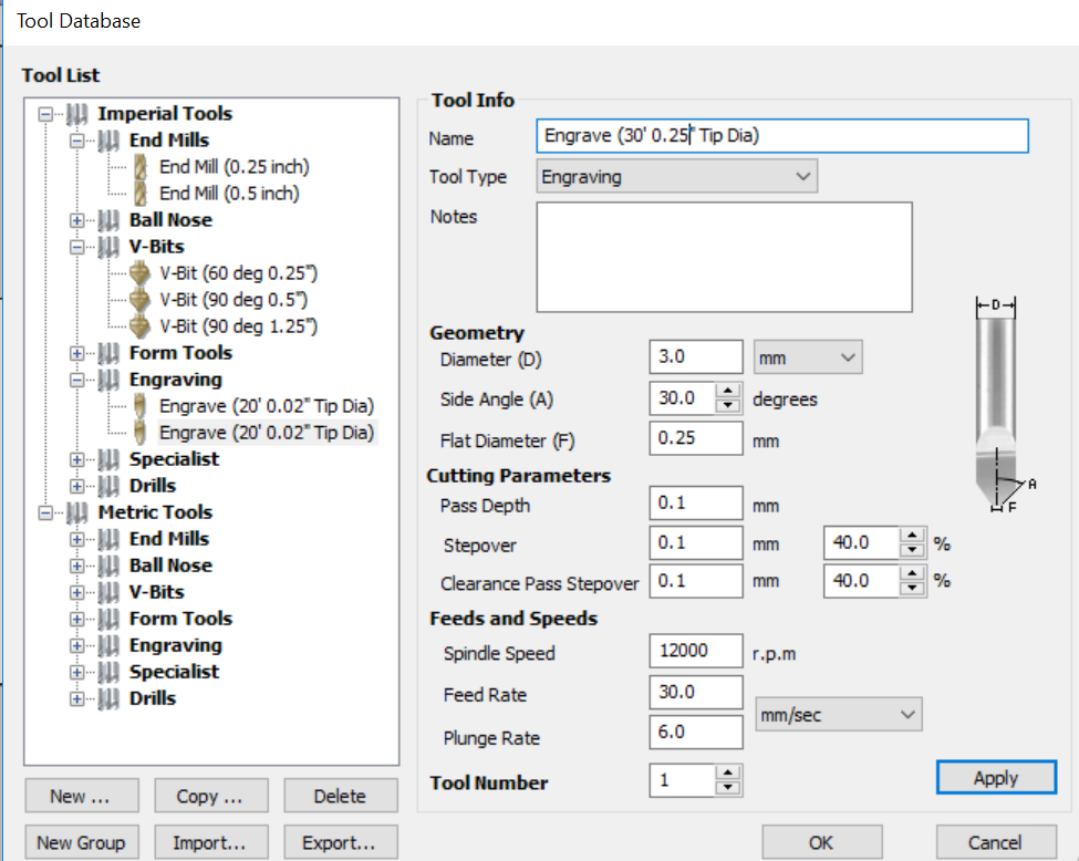
- Tool dimensions was set.
- Tracing the path of the mill.
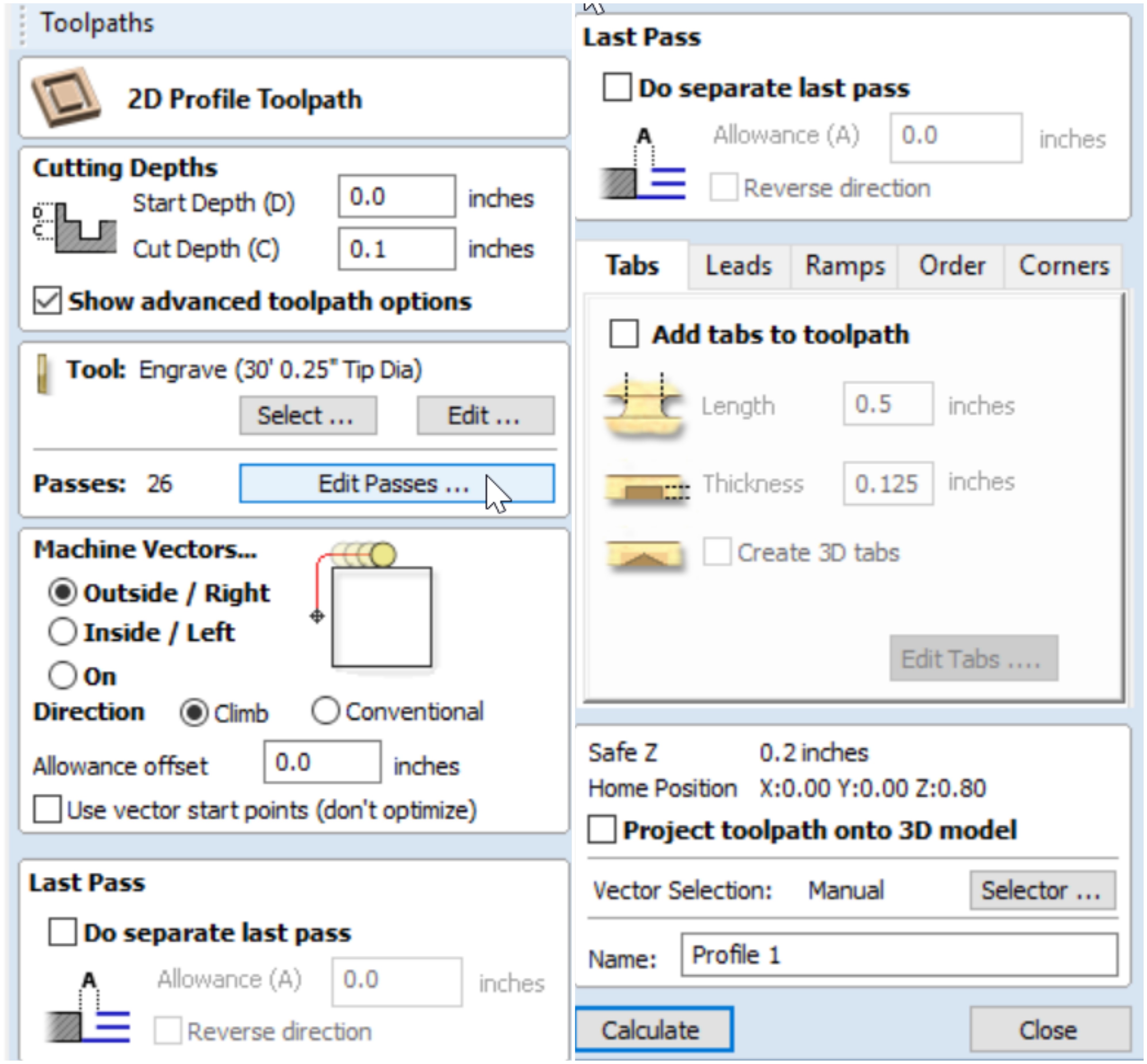
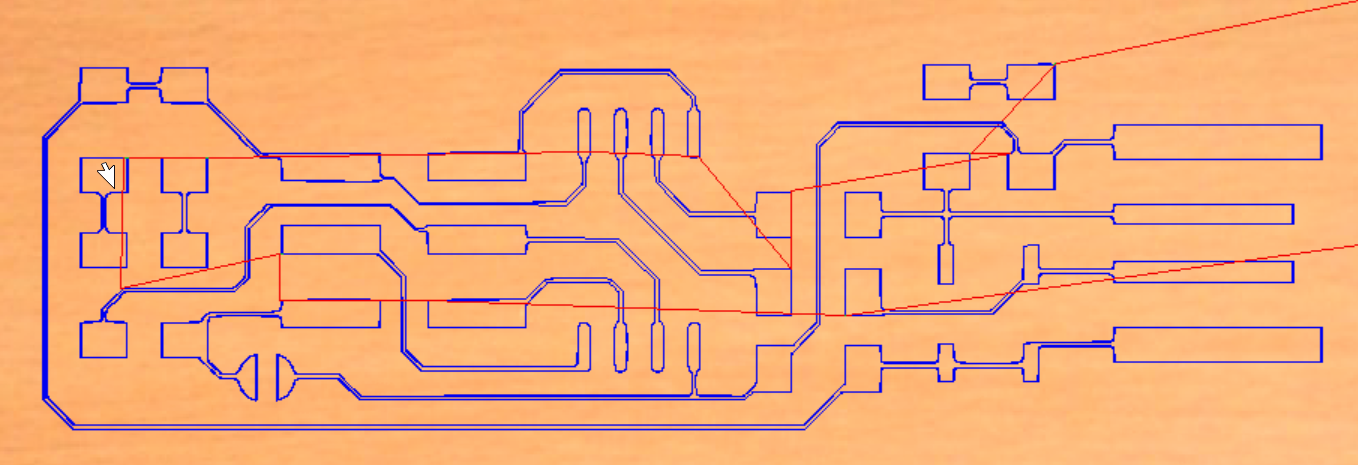
- Traceded path can be seen as below.
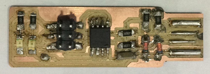
Mounting the Components
Following components are soldered on the PCB, very carefully.
- 2x 1kohm resistors
- 2x 499ohm resistors
- 2x 49ohm resistors
- 2x 3.3v zener diodes
- 1x red LED
- 1x green LED
- 1x 100nF capacitor
- 1x 2x3 pin header
Points to ponder
- Utmost care should be taken while soldering the components because the working zone is very compact and chances of sorting is very high for first timers.
- While soldering, beware of the fumes might cause headache.
- Use twisers for holding and fixing the components.
- Since SMD components is being soldered, so it is advicable to use magnifying glasses for soldering because they are very tiny.
Programming ATtiny45
Steps
- First step is to install avrdude by the following command line in Terminal.

- Next step is to download the firmwware source code. It can be downloaded from the following link.
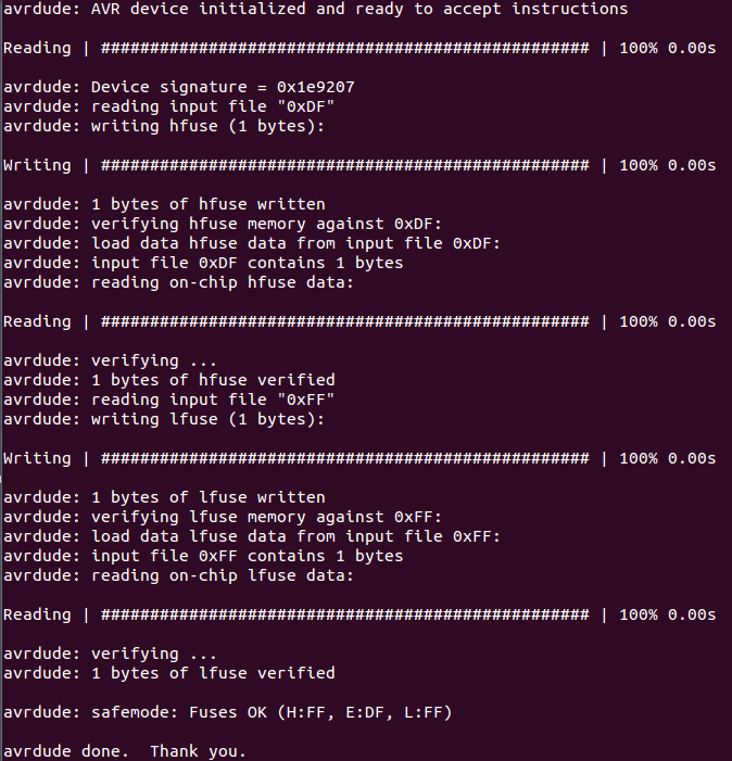
- Now, I connected my ISP with my Instructor's ISP to program it. Afterwards, I executed the command "make flash" in bash. This will erase the target chip, and program its flash memory with the contents of the .hex file you built before.
- Run the make fuses command and connect your ISP directly to the computer.
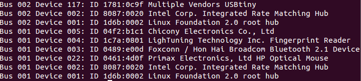
- Type lsusb in the terminal, which will list USB devices connected to your system. Mine was not showing in the list.
- I tried to debug my ISP but didn't find any luck. So, I developed Neil's ISP.
Making Neil's Board
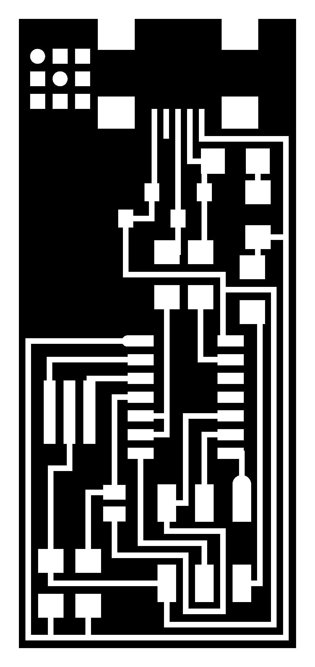
This time I milled my board on Roland SRM 20 machine. I downloaded .png images for traces and outline of Neil's ISP from the archive as shown below.
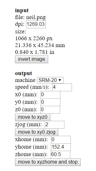
Using FabModule for creating .rml files
Steps
- To route your board, Downloaded .png files are fed to Fabmodule one by one.
- Output is set as .rml in Fabmodule.
- Process are set as "PCB Traces (1/64)" for milling traces and "PCB outline (1/32) for milling outline".
Machine Used
Cutting Parameters
- For Traces
- For Outline
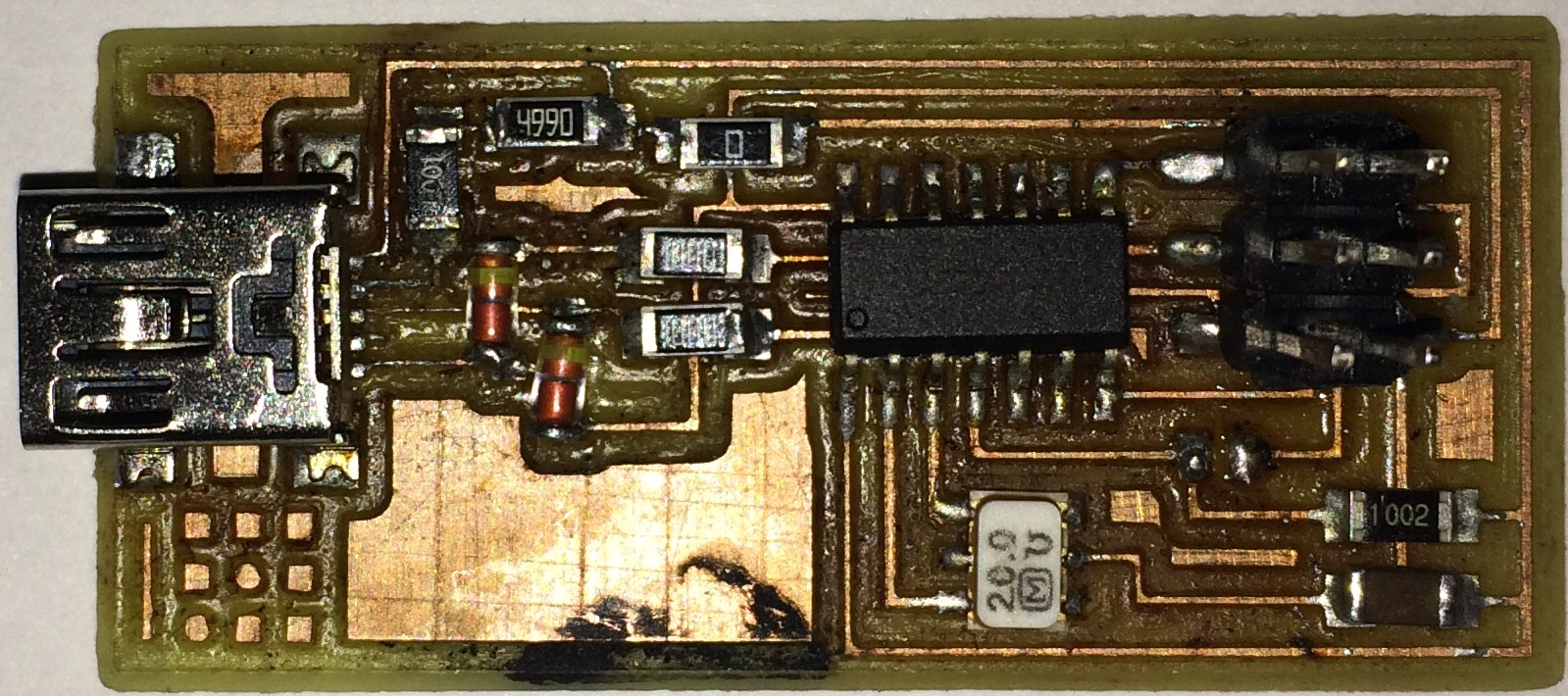
Components mounted on Neil's Board
Following components are soldered on Neil's Board.
- 1x 1kohm resistors.
- 1x 499ohm resistors.
- 2x 10kohm resistors.
- 2x 100ohm resistors.
- 1x 0ohm resistors.
- 2x 3.3v zener diodes.
- 1x 20 MHz Resonator.
- 1x 1000nF capacitor.
- 1x 2x3 pin header.
Stuffed Board
Programming The Board
Steps
- Download Firmware for Neil's Board.
- Add zero ohm resistor on SJ2 and short SJ1.
- Install AVR dude, it is already install in my computer.
- Now, I Connected my ISP with my Instructor's ISP to program it. Afterwards, I executed the following commands.
- Make Clean
- Make Hex
- Now go to the make file generate in folder and open it with text editor. Replace this line in the make file:
#AVRDUDE = avrdude -c avrisp2 -P usb -p $(DEVICE) # edit this line for your programmer (FabISP in our case)
AVRDUDE = avrdude -c usbtiny -P usb -p $(DEVICE)
Save the file and close.
- Now, connect your board directly to the laptop and continue to enter the following lines in folder opened in terminal.
- make fuse
- sudo make program
- Now use command "lsusb" to check, wheather your usb is getting detected or not. Mine got detected, this time.
- Final step is desodler SJ1 jumper shorting and board is ready to use.