The assignment for this week was to design and build a wired &/or wireless network connecting at least two processors.
My Approach
Will make two boards, bridge and node. The bridge board will connect the computer to the network of microcontrollers through ftdi cable and the node is connected to the bridge through 4 pin connector having VCC, GND, RX AND TX connections.
Will describe my design, fabrication process and approach toward the problem.
Will disucss arduino programming and document it.
Illustrate the problems faced and how they were tackled.
Bridge Board Designing
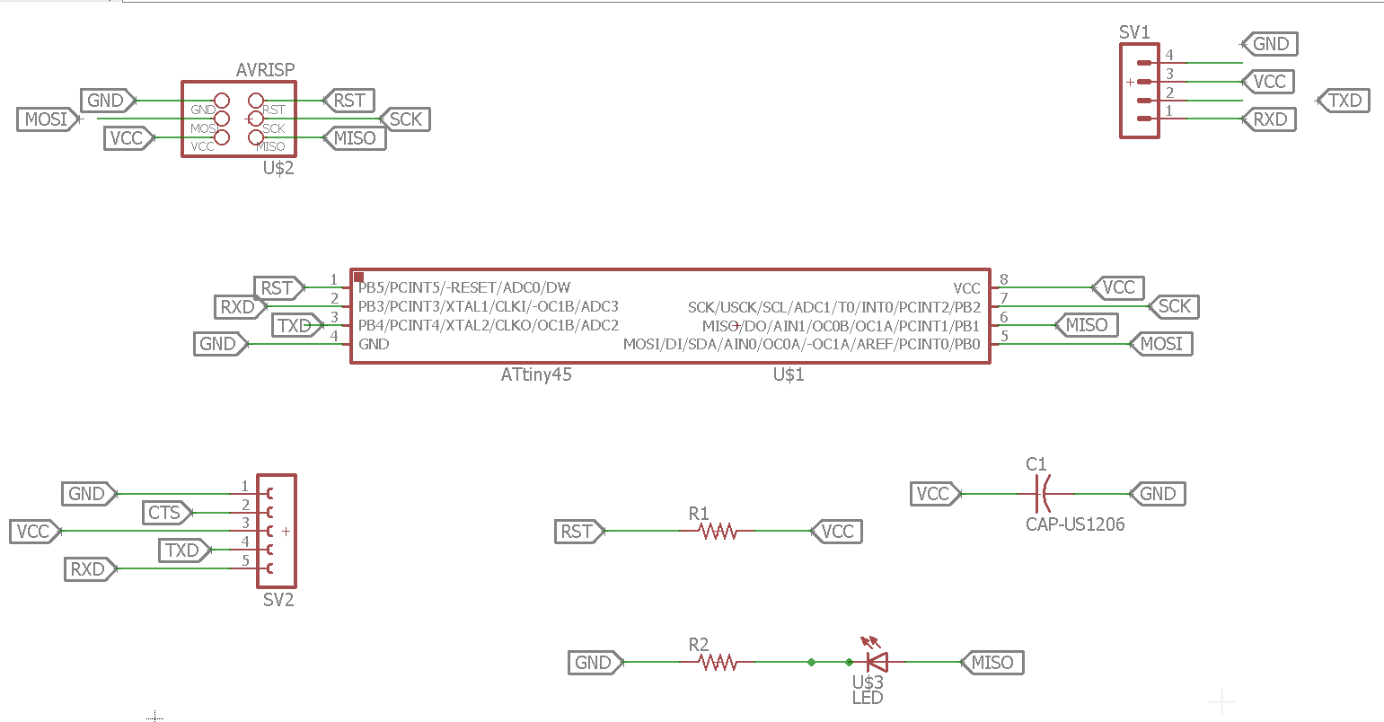
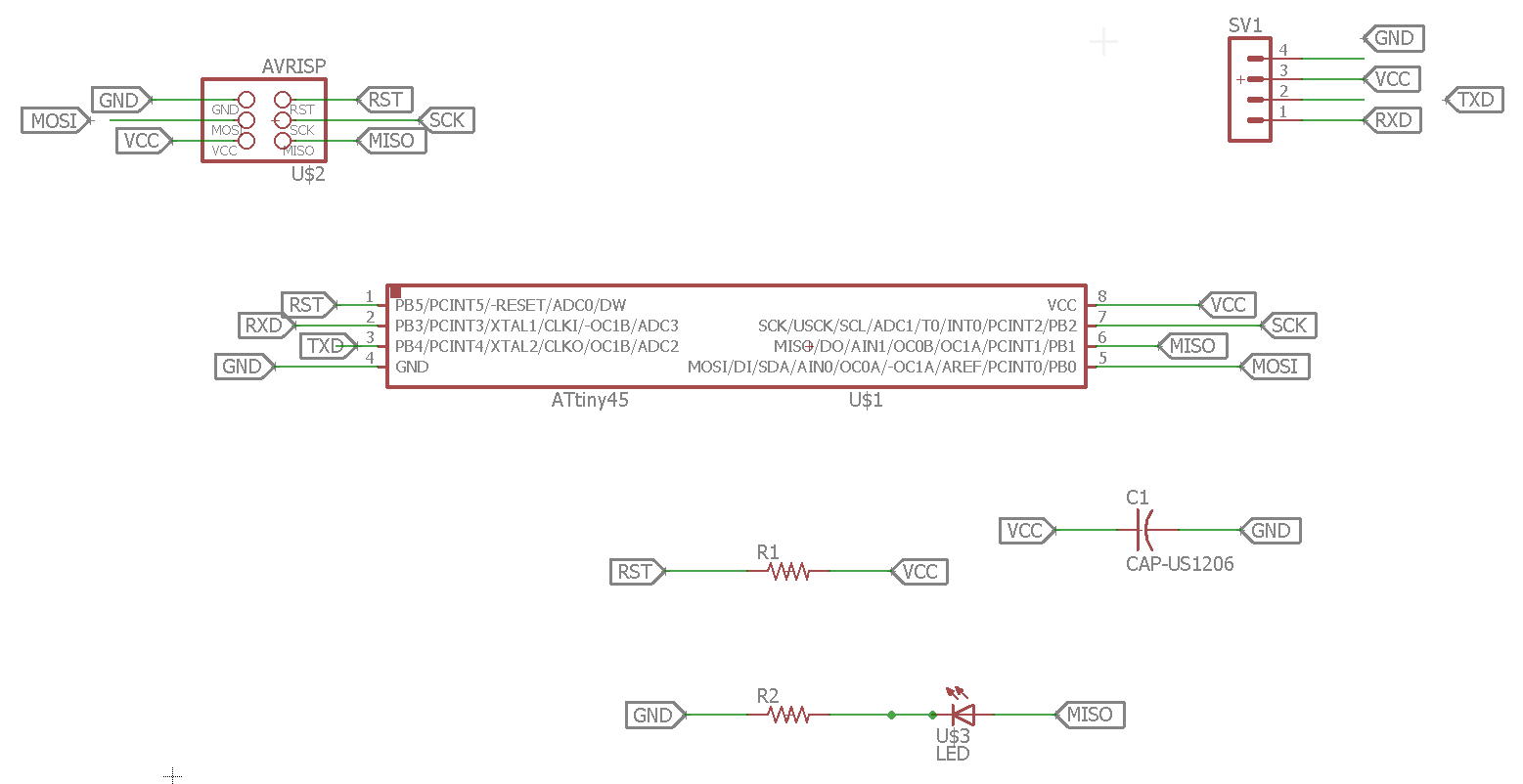
I took inspiration from Neil's hello.bus.45.bridge.cad for designing my board and redesigned it. Initially, I decided the components, I am going to stuff in my board i.e.
Attiny 45
1 1k Resistor.
1 10k Resistor.
1 1 microfarad Capacitor.
1 Led.
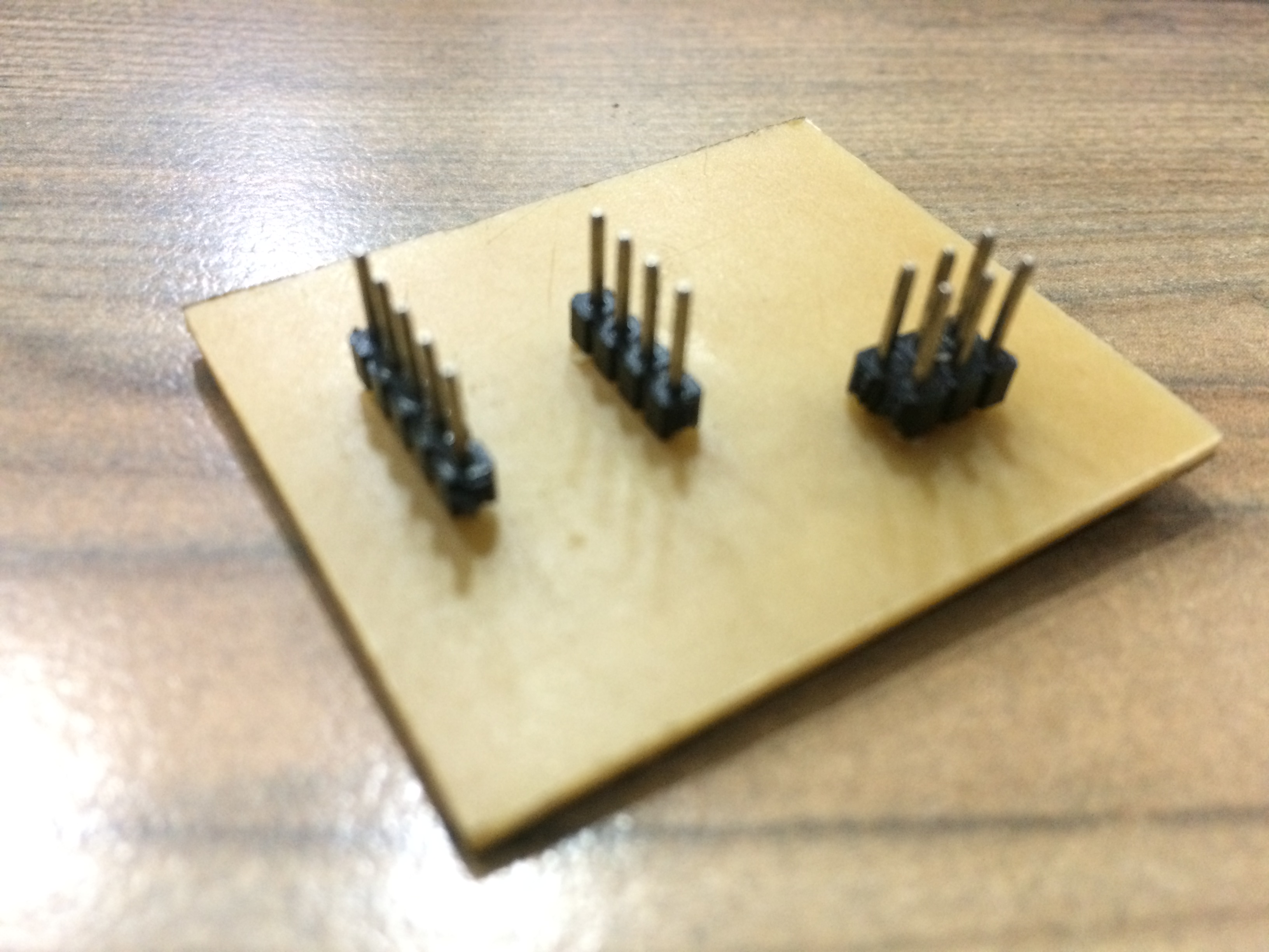
1 1x6 pin header for FTDI.
1 2x3 pin header for connecting FabISP.
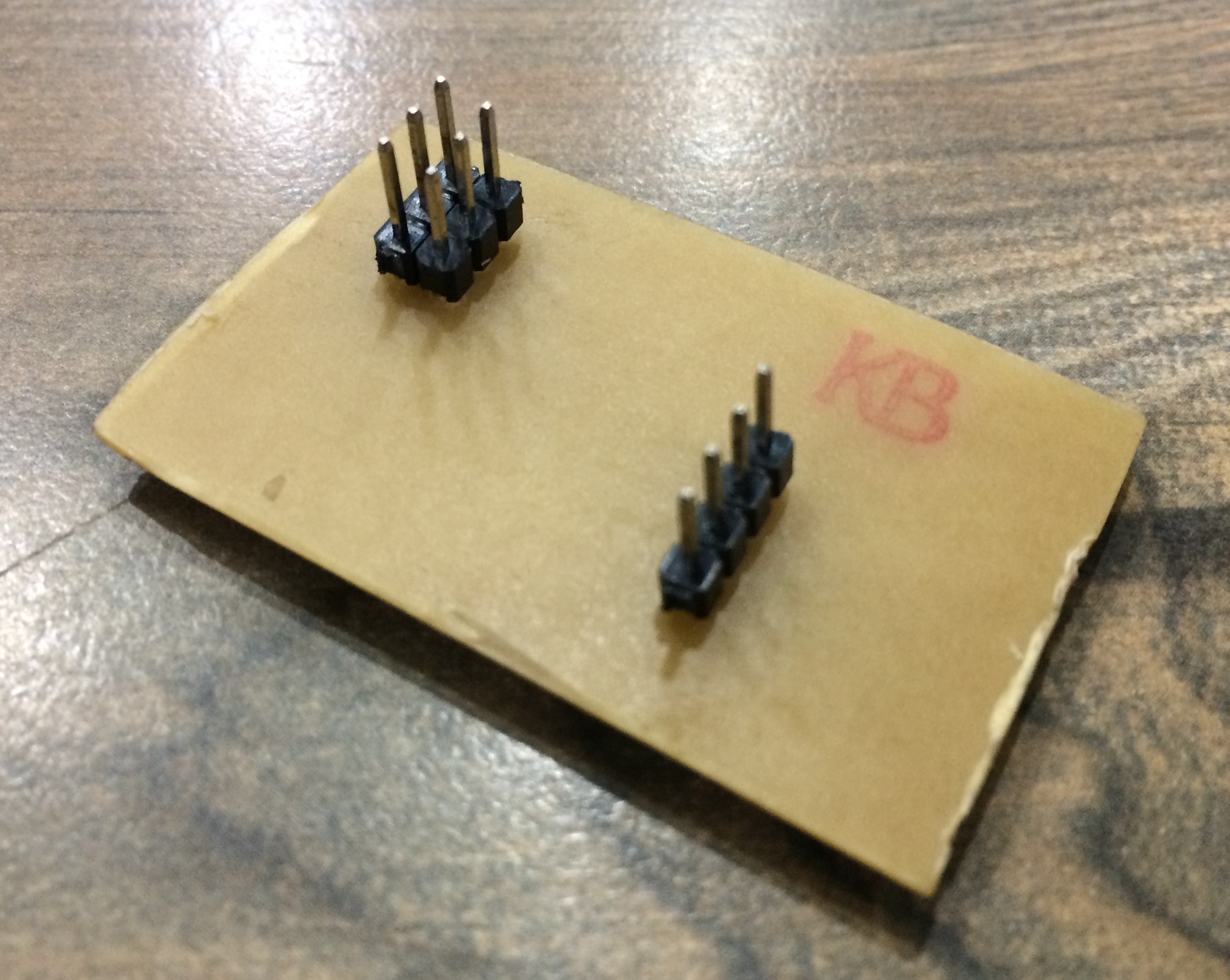
1 4x1 pin header for serial communication.
Afterwards on Eagle 8.0.2, I created my schematic as shown below.
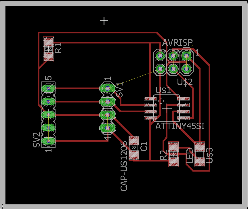
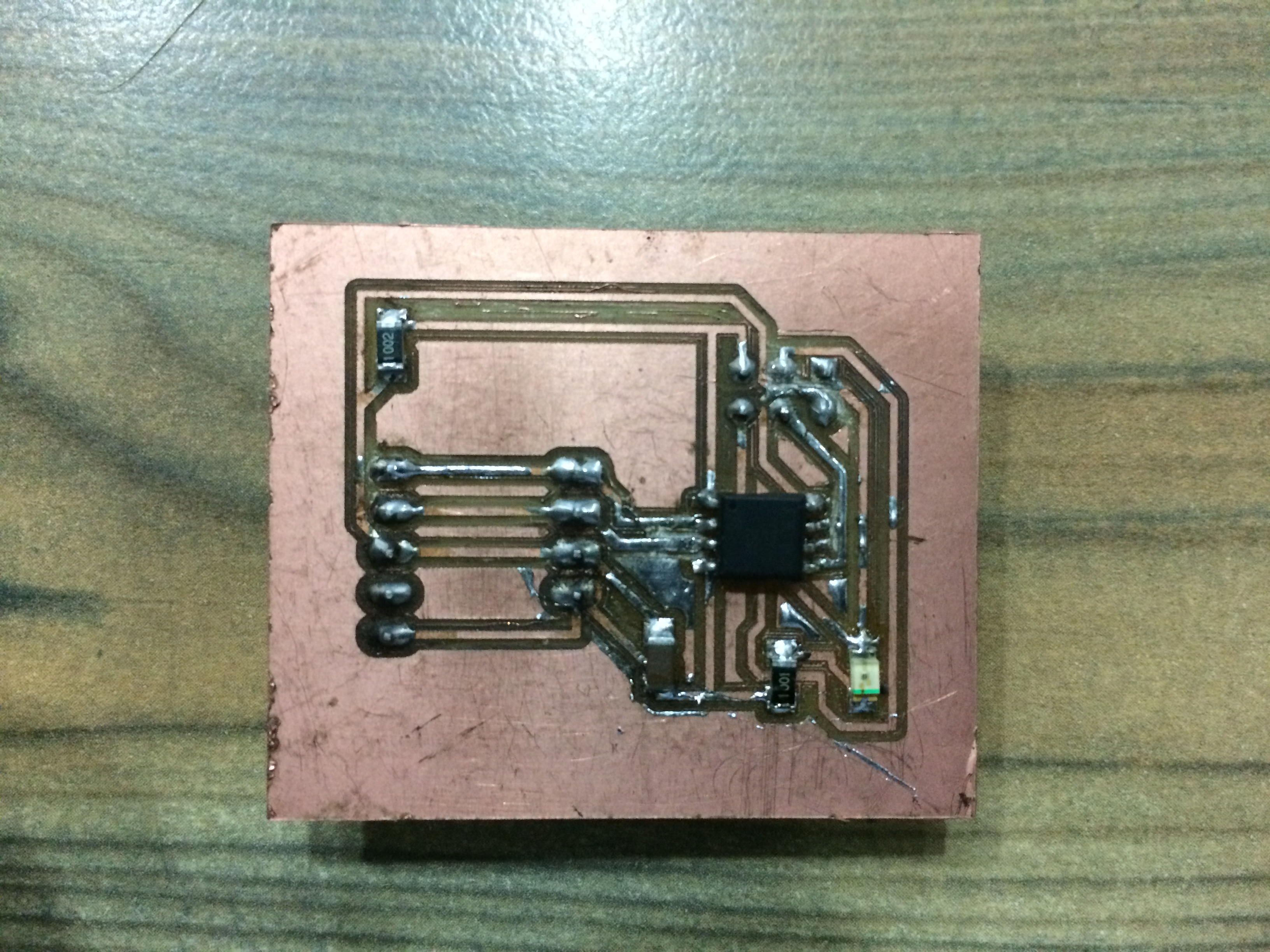
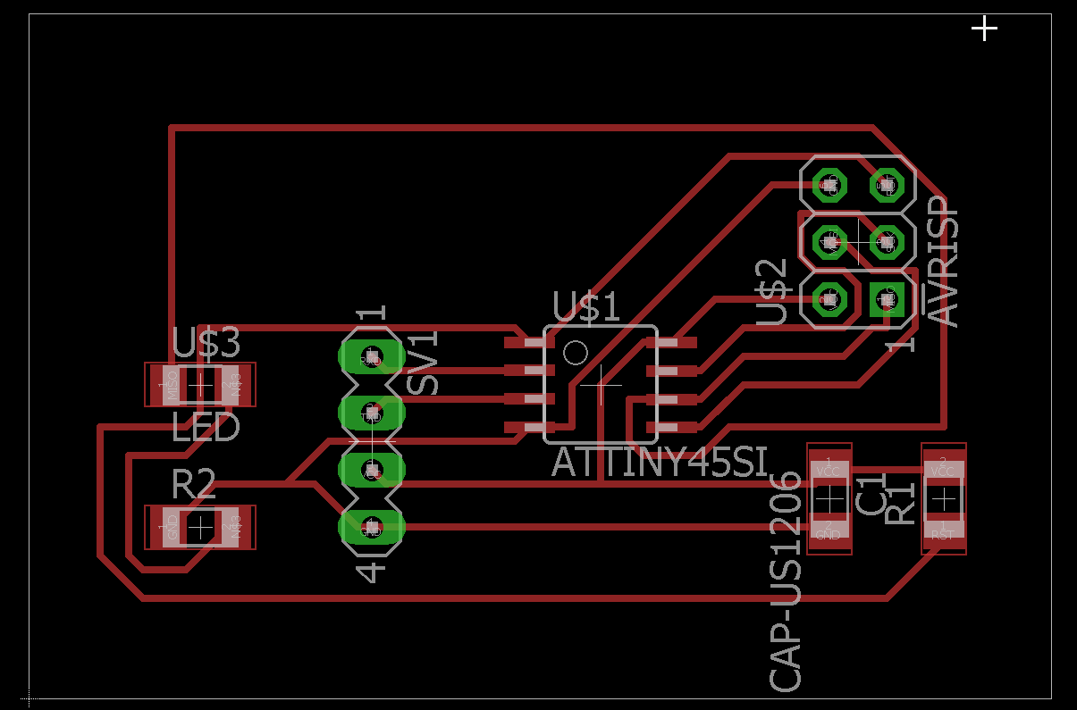
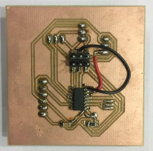
Using Roland SRM 20 machine, board was milled in the similar fashion as done in previous assignments. Also, the cutting parameters for Traces and Outlines are kept same as in Input devices assignment board.
Testing the Board
Step 1
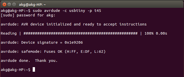
After stuffing the board with all the required components, I checked the fuses by the linux command as shown below.
Step 2
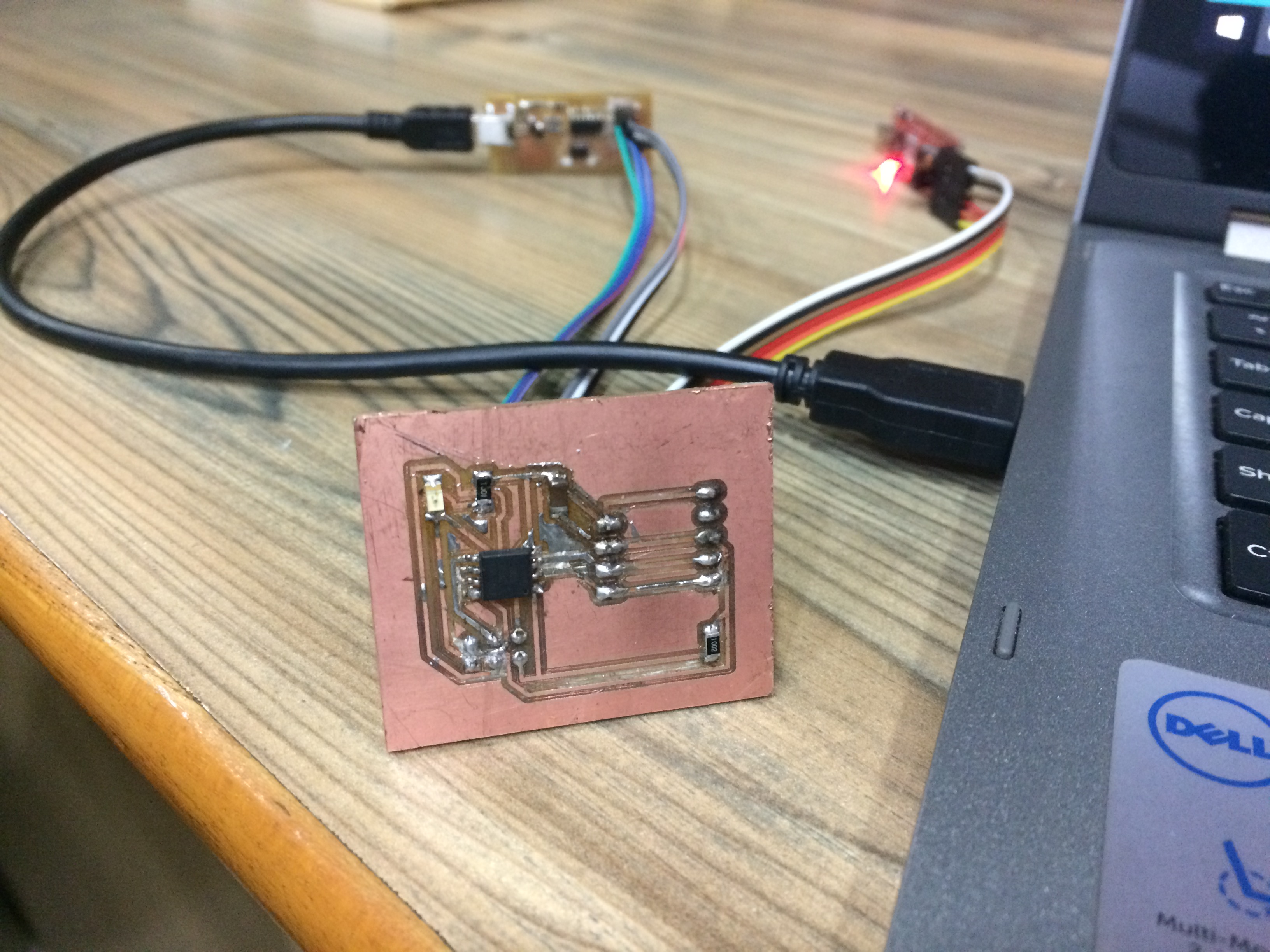
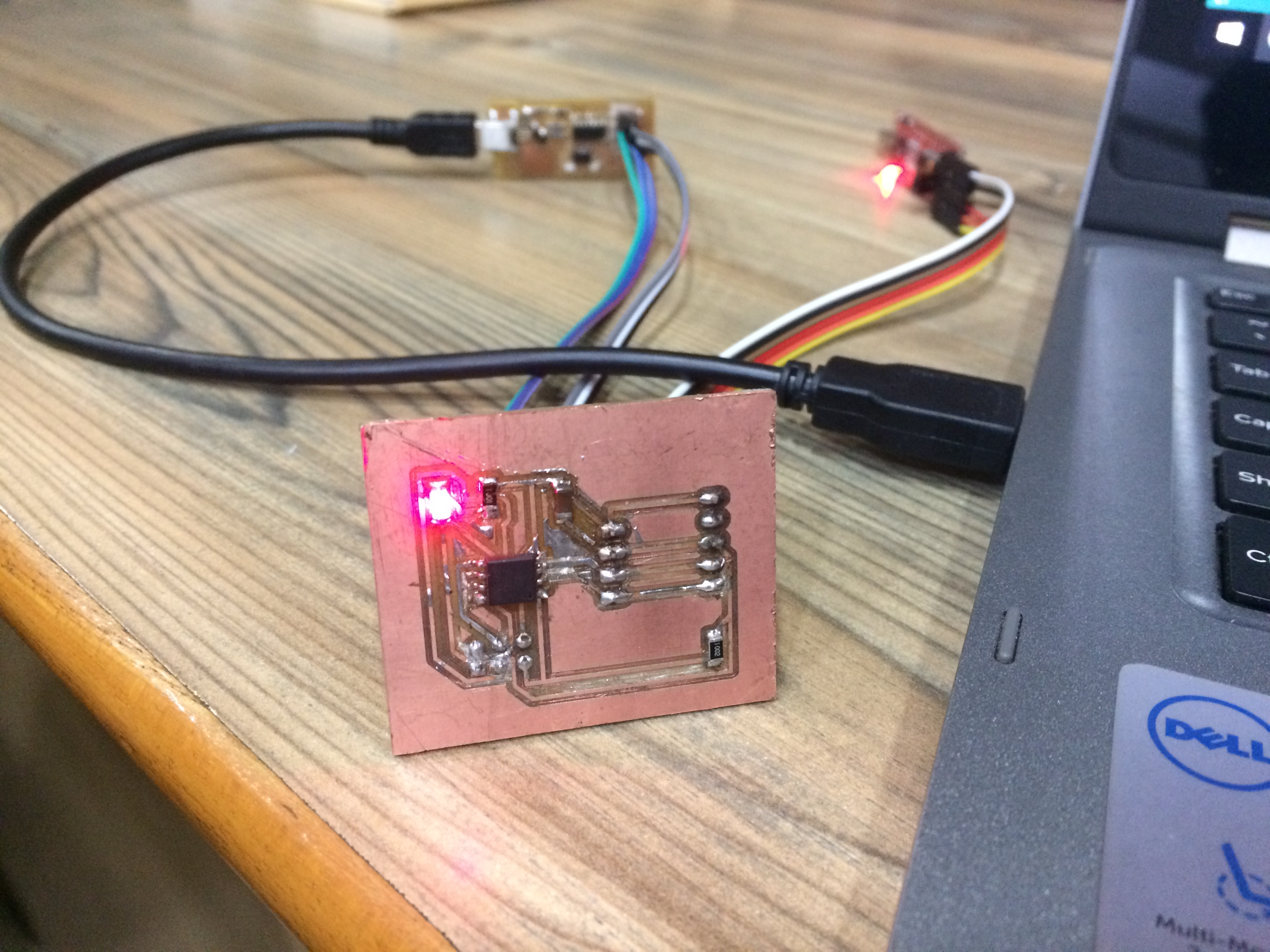
Afterwards I burned a blink Led program into the microcontroller and it worked perfectly fine.
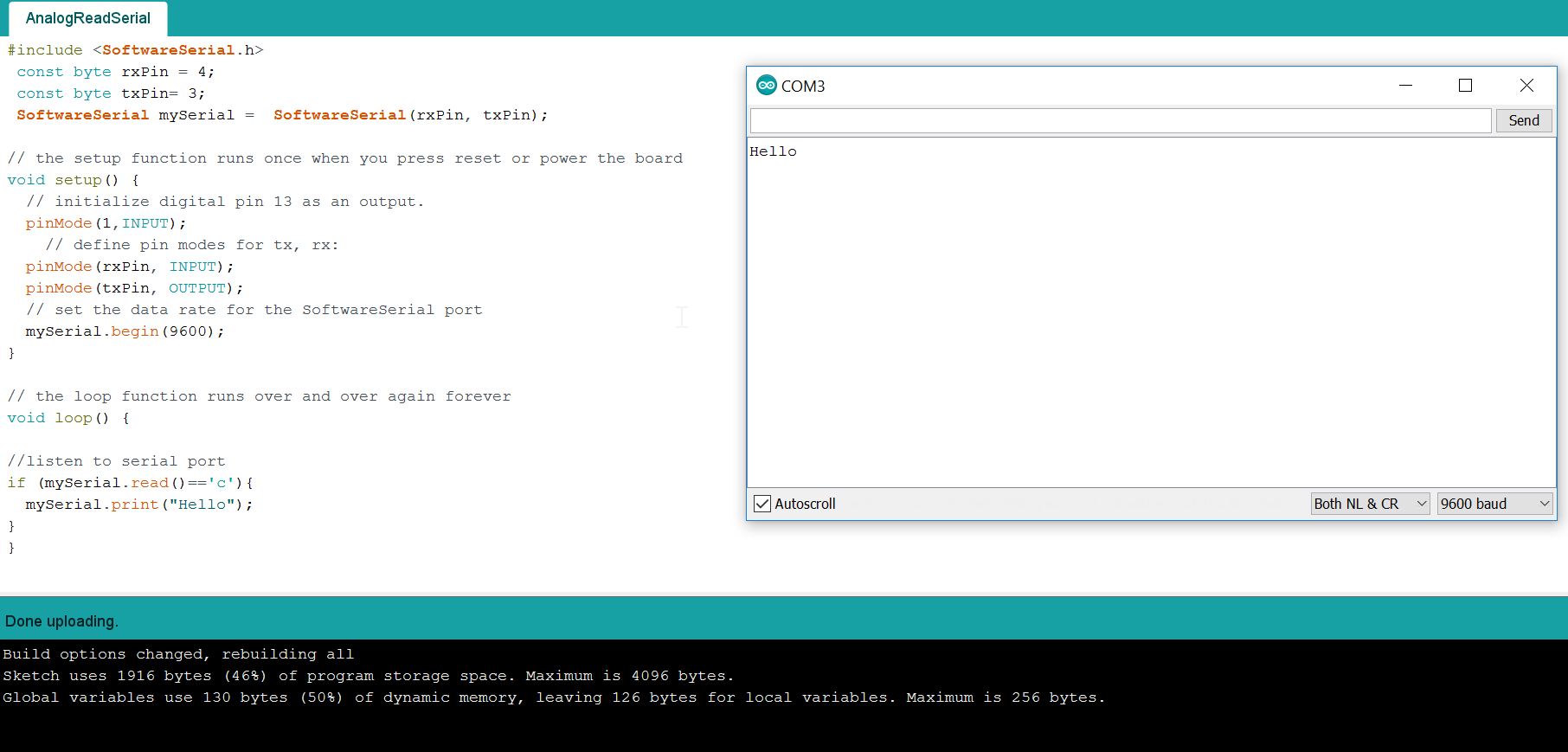
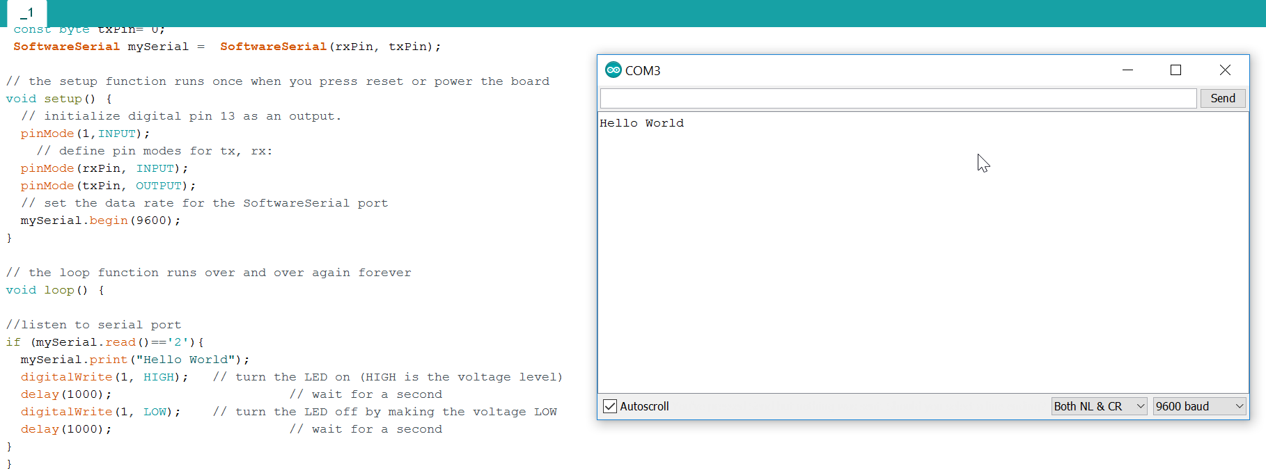
To check the serial communication with the board, I wrote one program to display "Hello" on serial monitor when c is given as input.
Node Board Designing
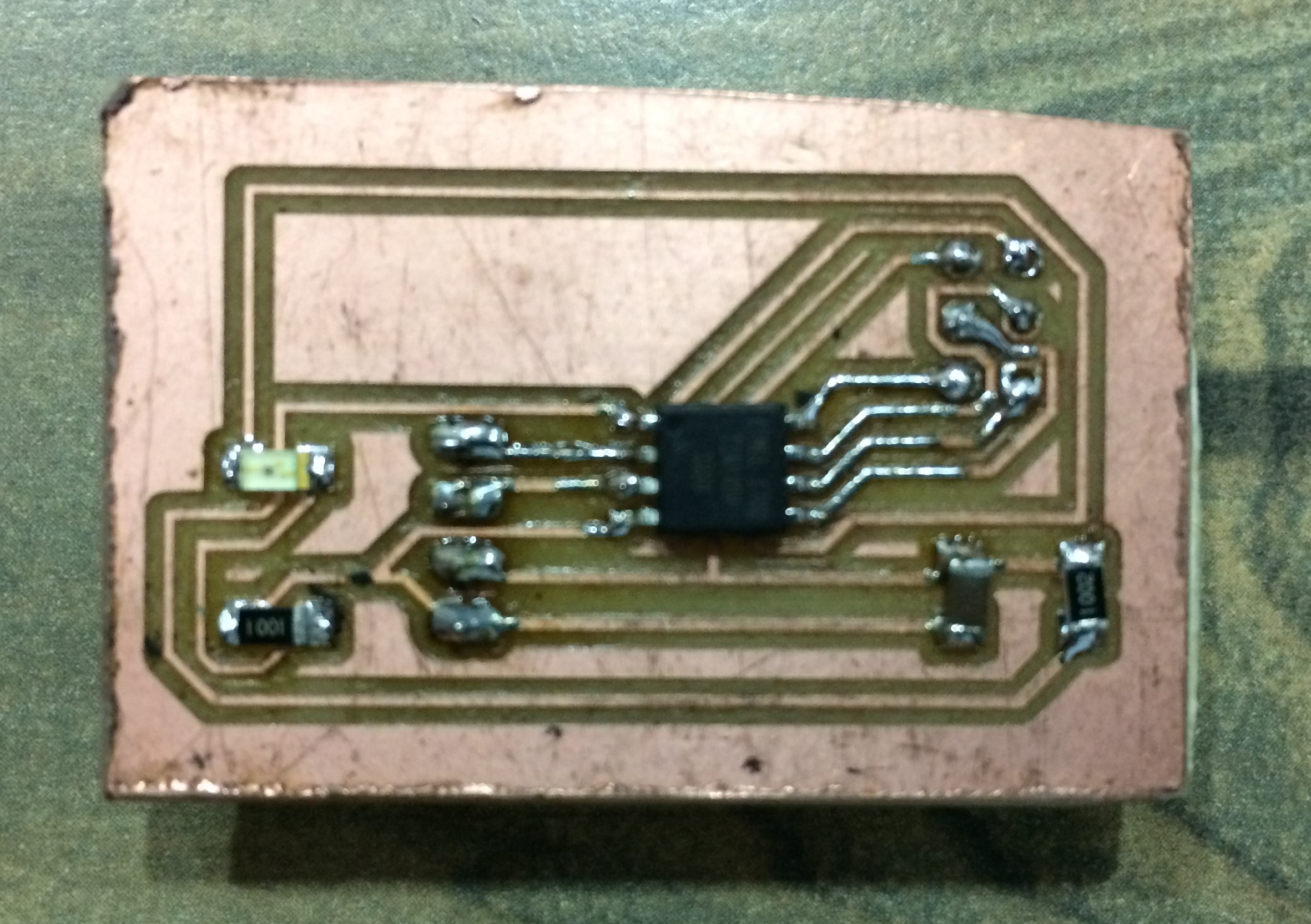
I thought of using my input devices board as node board, but it didn't worked in the network, although it was working fine in isolation. All the observations related with the input devices board is documented subsequently. Since, my input device board didn't worked. So, in consultation with my instructor I made one more board similar to the brigde board and just removed the 1X6 pin connector for FTDI.
on Eagle 8.0.2, I edited the schematic of the bridge board and created new board as shown below.
Problems with Input Device board to use as node board
I thought of using the following board as node board. This same board was used in Output devices as well as in Input devices assignments. I checked the serial communiacation with this board and it was working fine, as shown below. But, when I connected my bridge and node board in network both of them were not responding, the probable reason for this might be the variation in frequency because RS232 communicates in frequency form. Also Arduino code was not effective in producing PWM frequency, this problem I faced during my input devices assignment also. So, to overcome this problem I made a new board and used Neil's C code with some manipulations.
Milling and stuffing the Node Board
Using Roland Roland SRM 20 machine, board was milled in the similar fashion as done for bridge board. Also, the cutting parameters for Traces and Outlines are kept same as for bridge board.
Testing the Board
Step 1
After stuffing the board with all the required components, I checked the fuses by the linux command as shown below.
Step 2
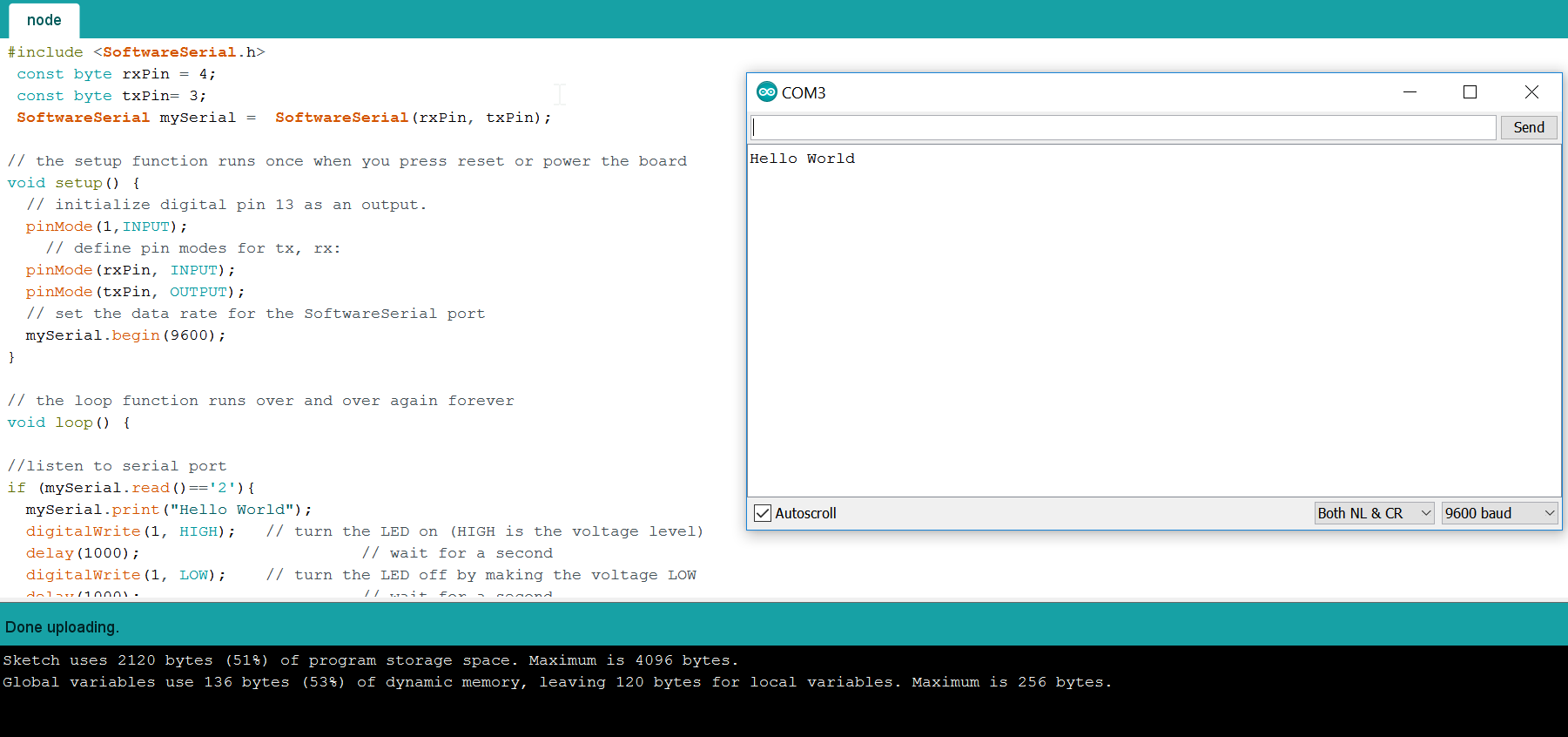
To check the serial communication with the board, I wrote on program to display "Hello World" on serial monitor when 2 is given as input.
Networking & Communications
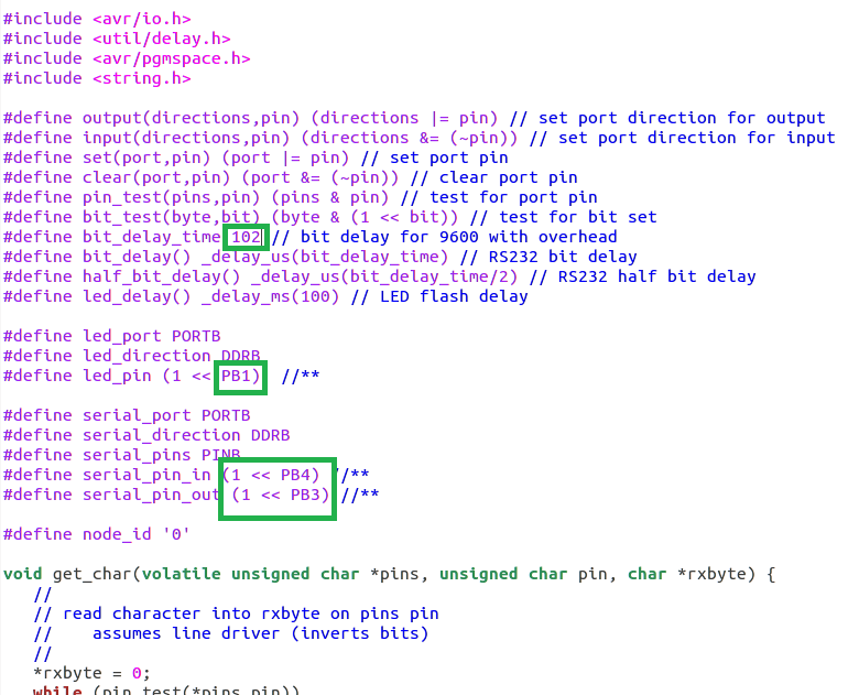
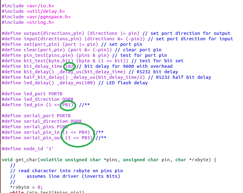
As I have already mentioned that arduino code was not effective in producing PWM frequency and this very same problem I faced during my input devices assignment also. So, to overcome this problem I burned Neil's C code in my bridge and node board with some manipulations as discussed below.
Changes done in Neil's C program
Rx, Tx & input to led was defined in the program in the form of corresponding pins. Also, bit delay time was increased from 100 to 102, to have proper display on the serial monitor. All the required manipulations done with the Neil's C code is shown below.