Electronic Production
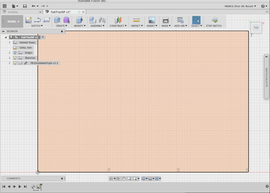
For Week 4 – Electronic Production, we decided to print the FabTinyISP
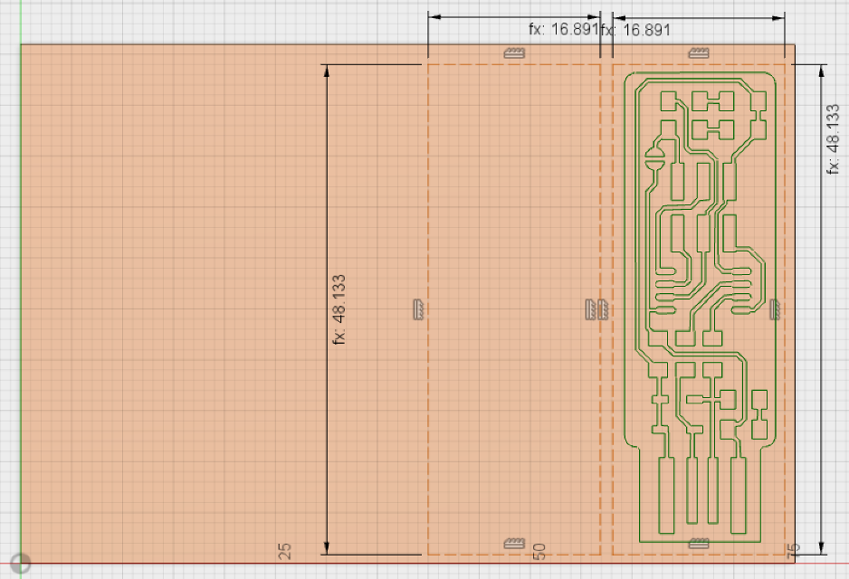
Before deciding on this, I tried to produce a board on the same design, but according to a layout of my own. Since this took too long, I switch gear and went back to the original assignment (more below on my attempt to use KiCAD for my own layout).We downloaded the PNG files for the traces and the outline.
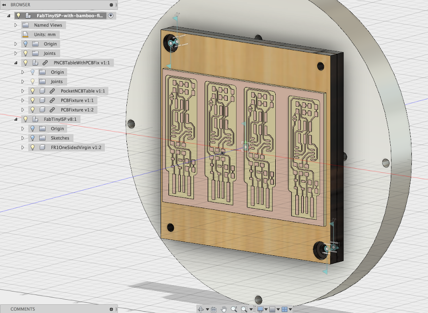
We had to make “sacrificial” mount or setup to put the board on, while the machine is milling. There was some a bamboo board lying around so we quickly designed a setup out of it, in RDWorks.
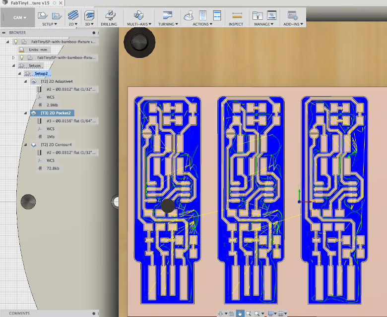
There are three steps to produce a PCB from FR1.
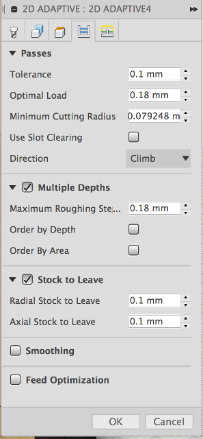
We need to do use three different methods 2D Adaptative Clearing (to remove most of material), 2D Pocket (to precisely define the traces) and 2D Contour to cut out the board(s). For each, we must define and go through the different tabs Tool, Geometry, Heights, Passes and Linking.
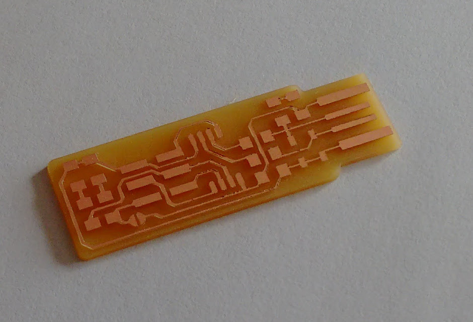
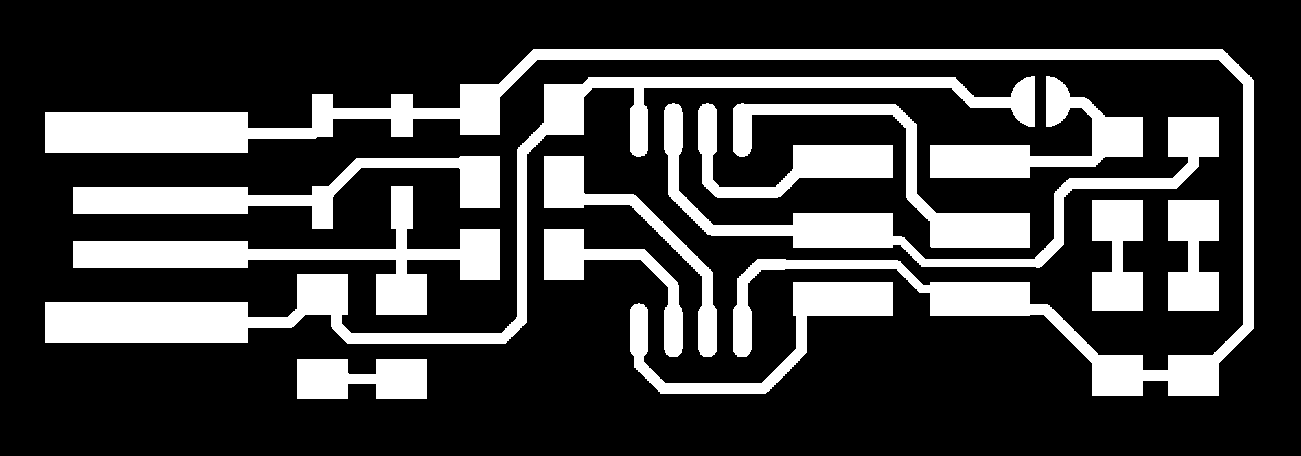
Here is the circuit after the milling.
An attempt at Circuit Design
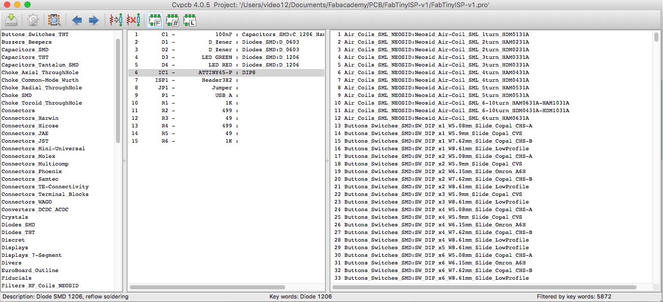
This week, I really wanted to mill my own circuit. So, before milling the PCB, I tried to design my own circuit. For this, I decided (arbitrarily) to use KiCAD, downloaded it and installed it.
I tried to find a video tutorial and settled on this really nice one, just to get a feel for KiCAD.
There are quite a few things to be mindful while using KiCAD for the first time – which the video tutorial touches upon–, but the software is well done and is quite quick to get a grip on.
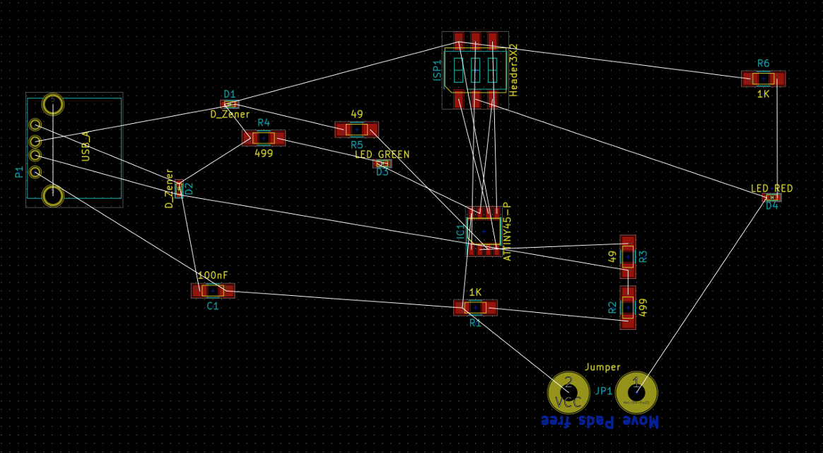
First, I redrew the schematics in KiCAD. I laid down the components.
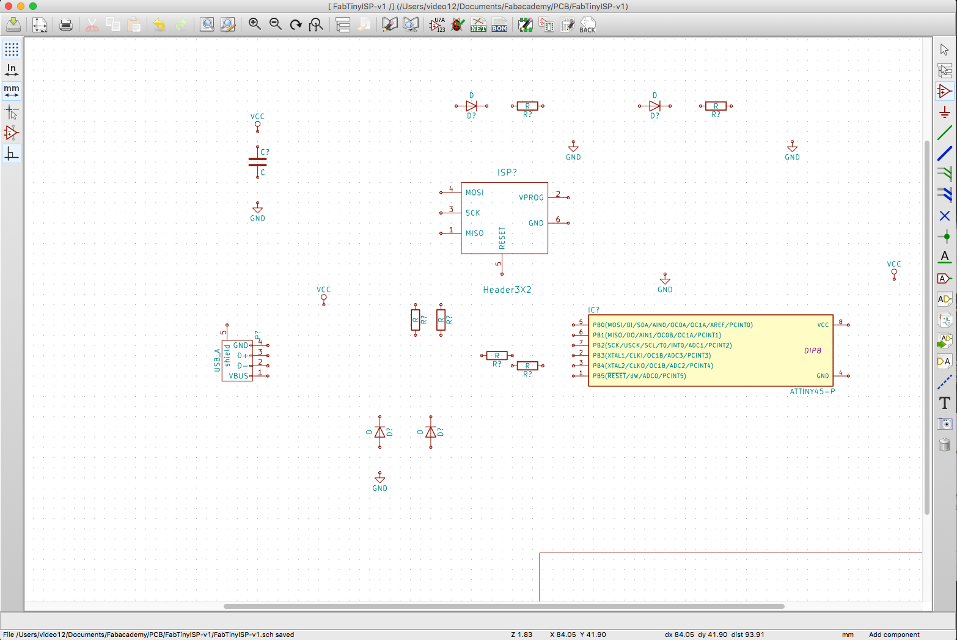
Then I drew the wiring schematics.
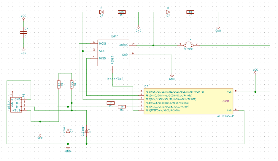
After that comes a step where you have to assign layout to each of the components on your schematics.
In the layout, you spread around the components and finish your design. By that time, the week was already well advanced and I decided to stop the design part and just concentrate on the core of this week's assignement - that is electronic production.