WEEK 6
ELECTRONICS DESIGN (WEEK 1 OF 2)
Assignment: Redraw the echo hello-world board and add at least a buttonand LED with current-limiting resistor or design your own.
Material: - soldering tools and components Softwares:
- Eagle, from CadSoft editor, CAD-Software for PCB design
- ArduinoIDE, for the programming
- Fab Modules, to prepare the files for the Roland (.rml)
DETAILS
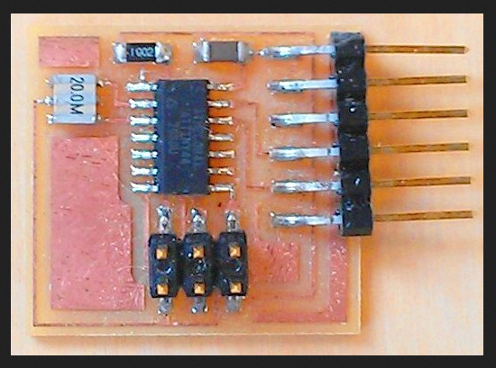
The Echo Hello-World Board (sources)
The aim is to re-draw the Echo Hello-World Board In order to do this, my sources were the following:
Source images:
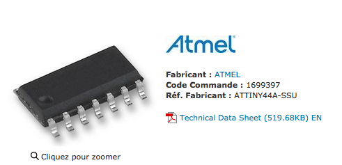
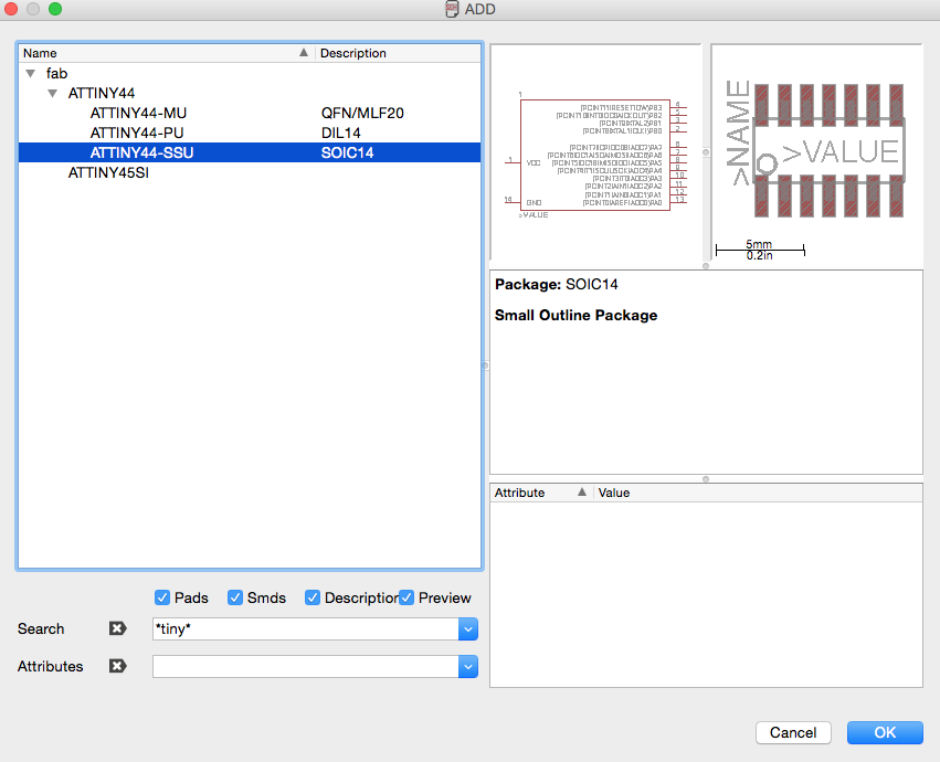
Model of Microcontroller: ATMEL ATTINY44A-SSU 8 Bit Microcontroller,Low Power High Performance, ATtiny, 20 MHz, 4 KB, 256 Byte, 14, SOIC
Here is the page with all information about it on farnell.com websiteIncluding the Technical DataSheet ... oups ... 286
pages for the full version!! ;-)
Installing Eagle software, and starting using it
|
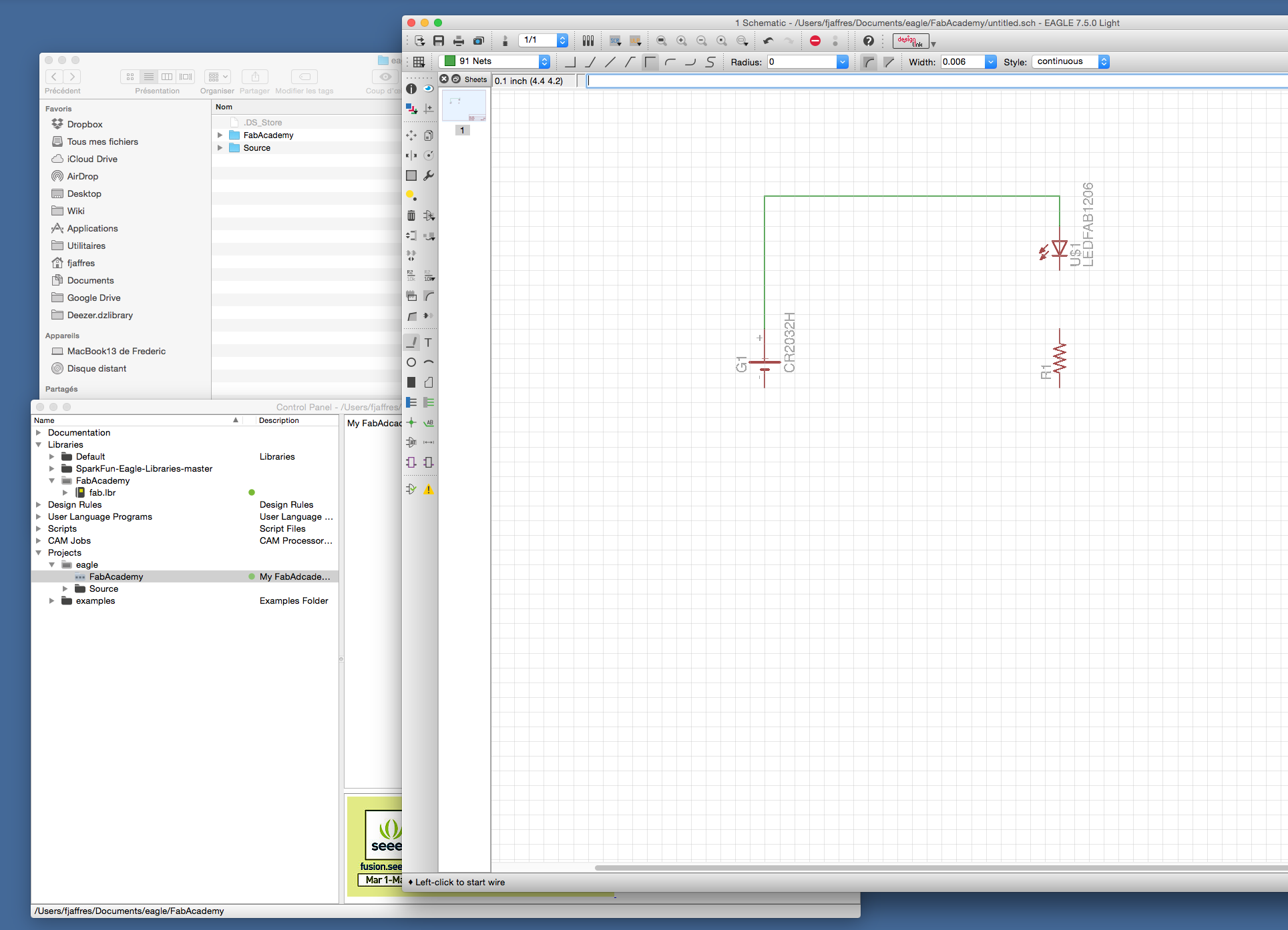
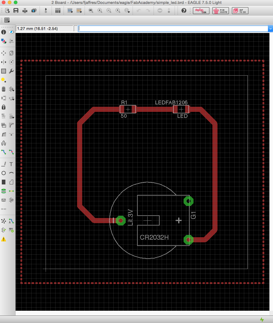
After installing the Eagle software,and the libraries (from SparkFun, and Fab Academy)now I can start using the software doing the 'simple led schema'
|
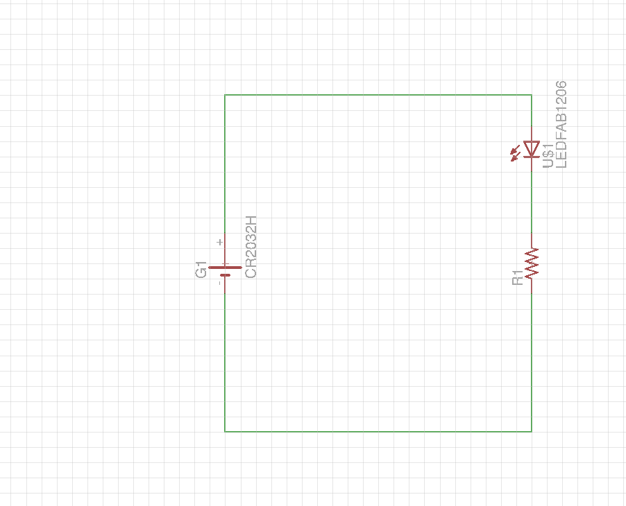
First we create a project, and then we start to do the SchematicHere is my Schematic for the 'simple led schema'We can test it with the ERC (Electrical Rule Check) when finished
|
|
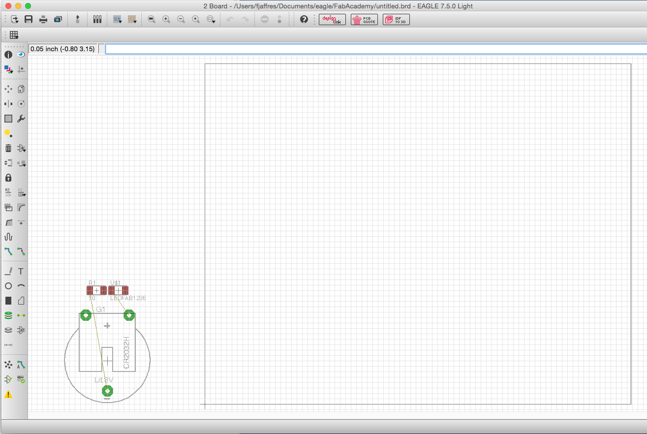
Then we switch to the Board viewand we start to design the boardfirst we move the components to the Board...
|
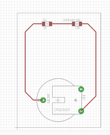
and then we do the routing between components
|
|
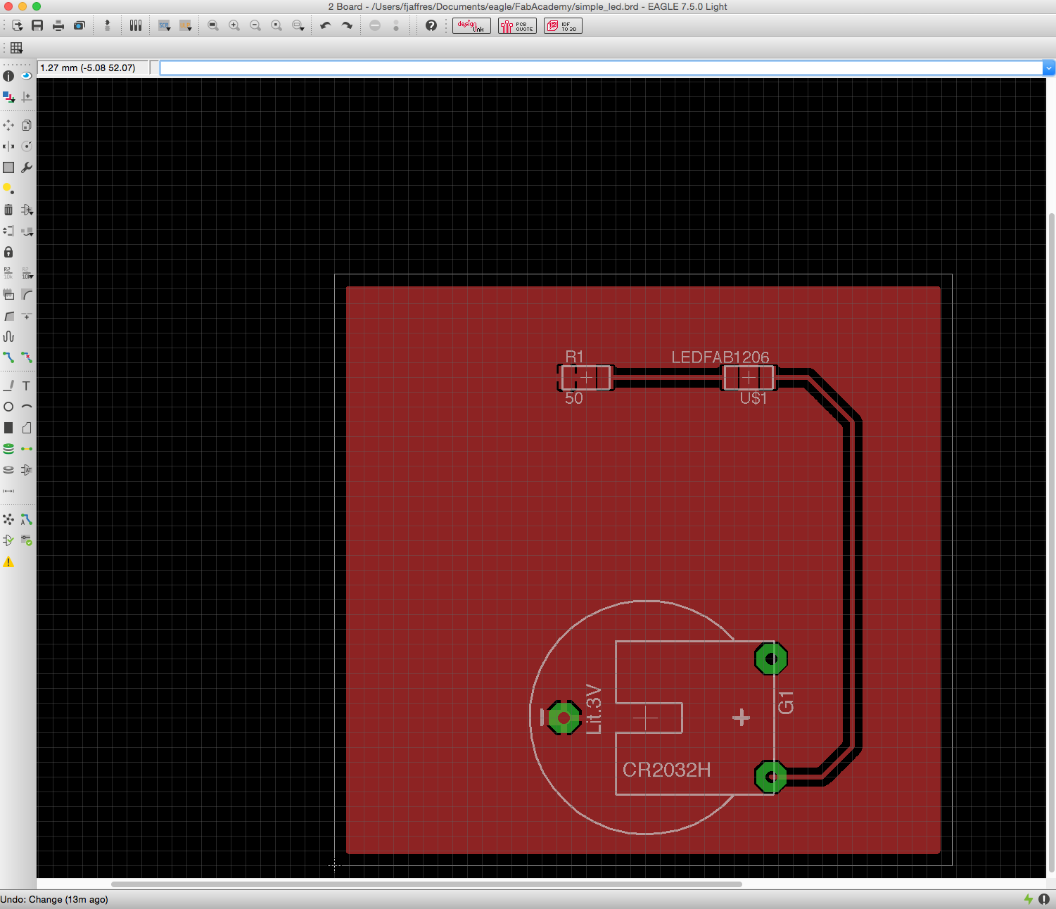
In order to create a groundplane we have to draw a polygon around the Board
|
And then using the Ratsnest function, it will automaticaly create the groundplane
|
Now doing the Echo Hello-World board (First Version)
|
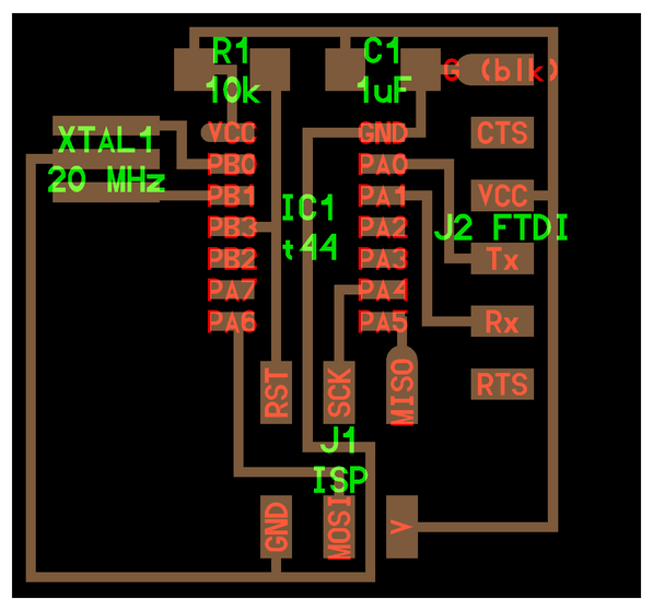
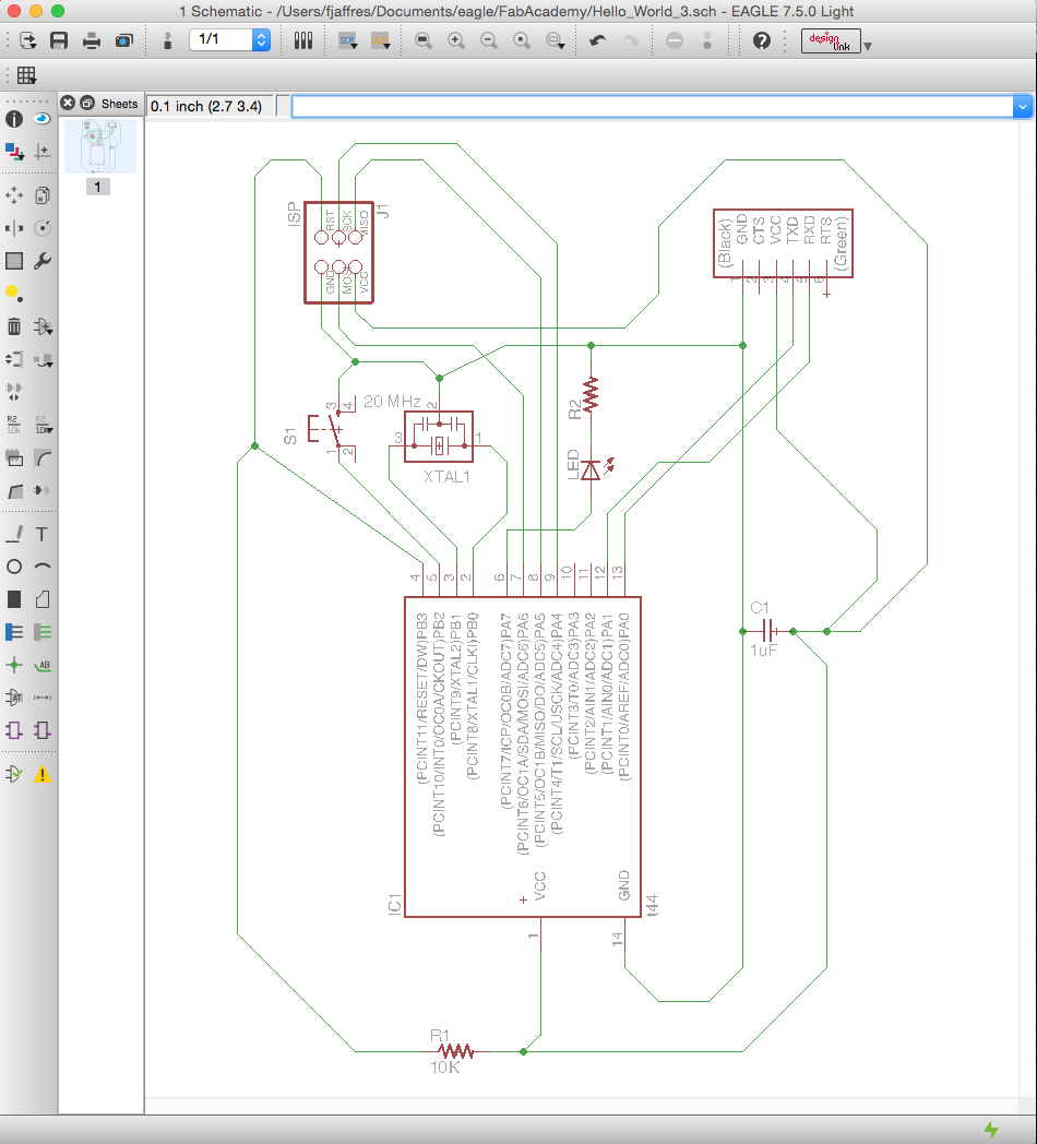
Here is my final Eagle SchematicIt includes the Button (switch) and the led+resistor schemaconnections to VCC and GND are not optimized, I should have used the copy feature to simplify with several VCC and GND objects,
next time I will do it :-)
|
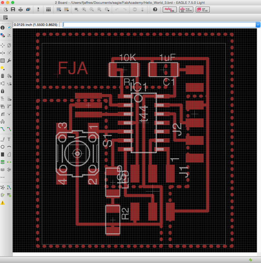
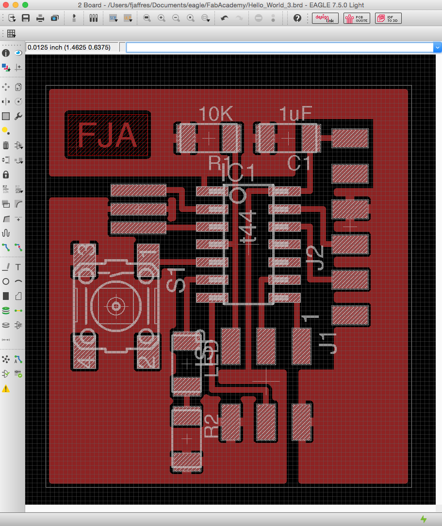
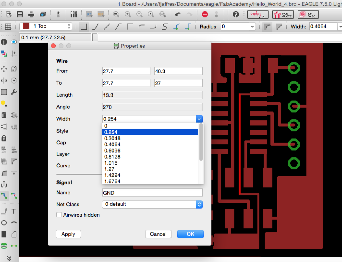
Here is my final Eagle BoardI created 2 polygons (one for VCC, one for GND), in order to minimize the drilling job
|
|
After applying Ratsnestand all layers displayed
|
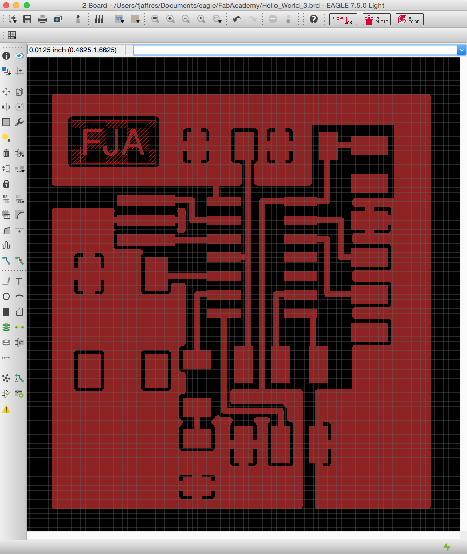
After applying Ratsnestand only top layer displayed
|
|
An example of interface will adding a component in Schematic view
|
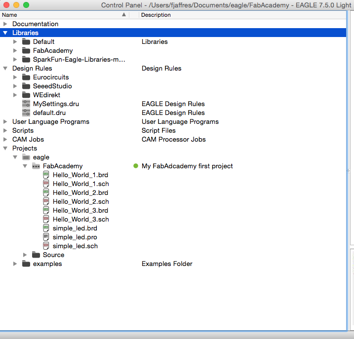
My configuration: Libraries, Design Rules (including MySettings.dru which is my resulting settings, inspired from SeeedStudio dru)...
|
|
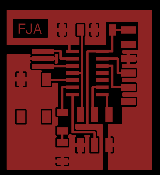
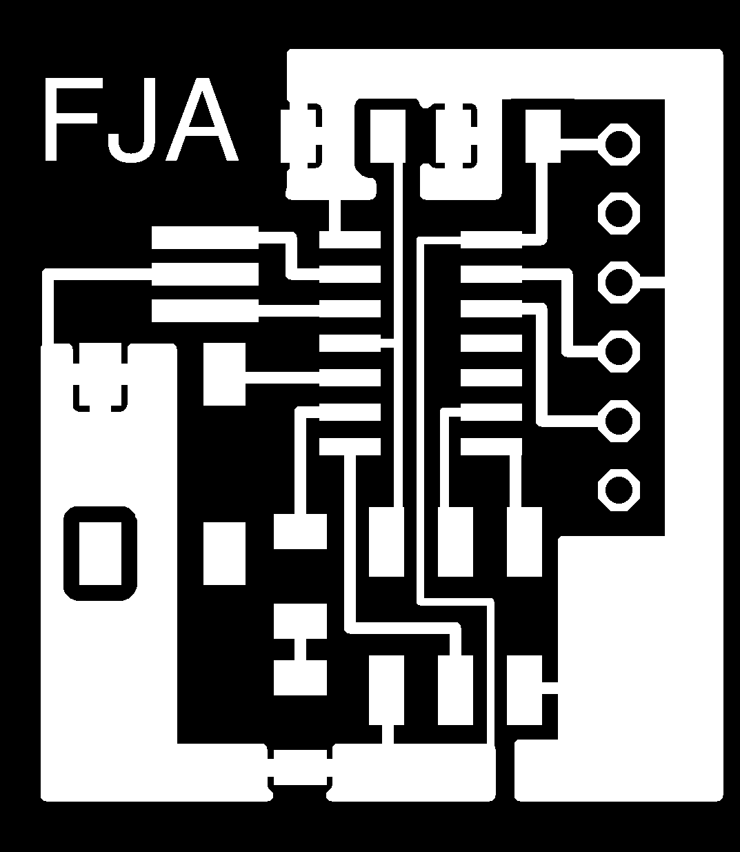
As a result, here is my PCB schema (.png export from Eagle)First version of my Hello Board Design
|
Milling and soldering the Echo Hello-World board (Final Version)
|
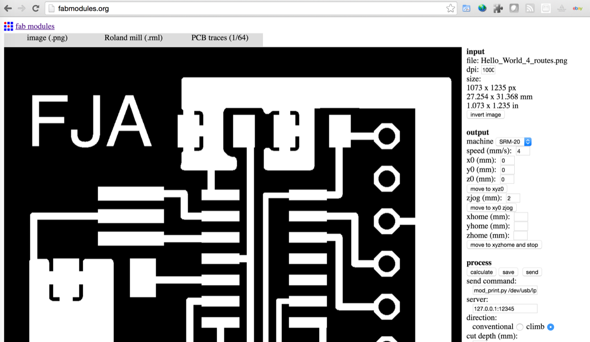
Working in Fabmoduleconfiguring
|
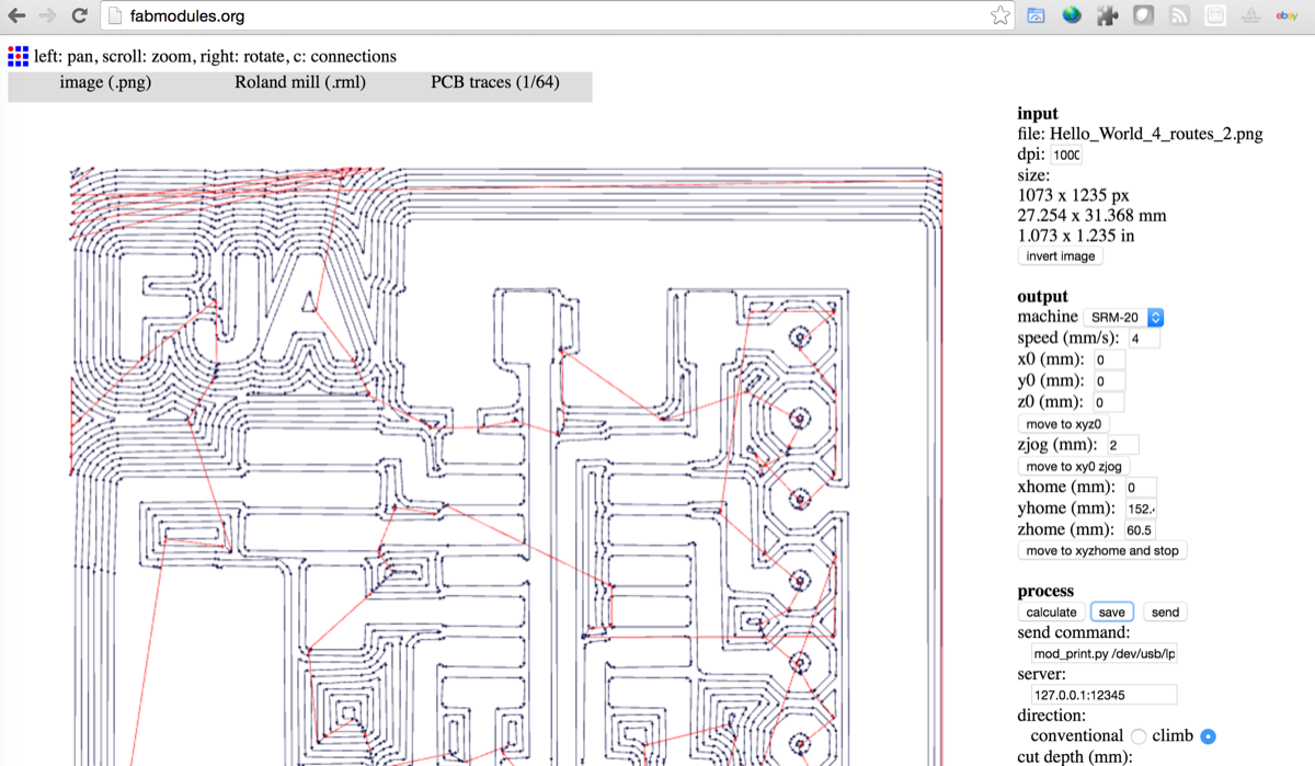
Here is preview of path
|
|
I had to minimize width of 1 tracebecause I got an error on Roland (that was not identify with the DRC in Eagle)
|
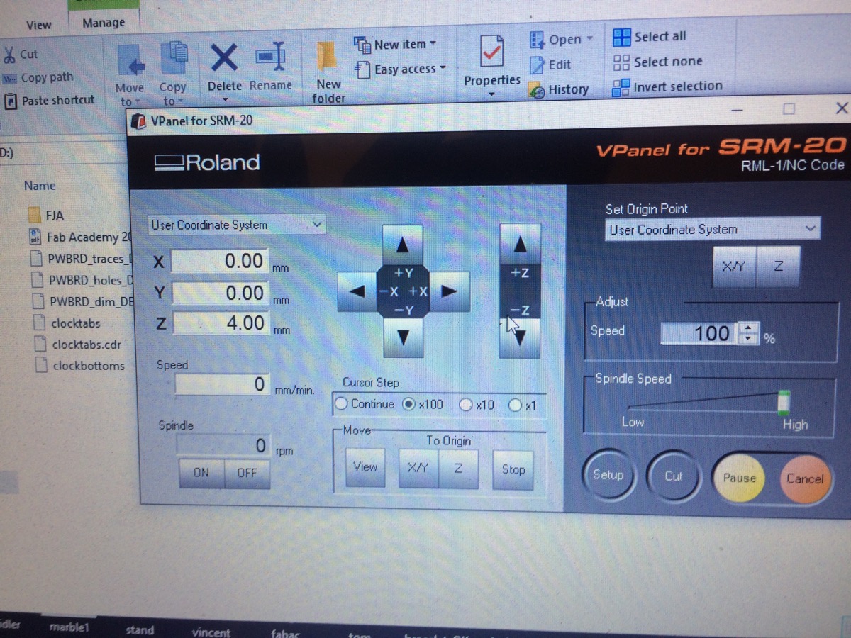
On the Rolandconfiguring X/Y/Z zero
|
|
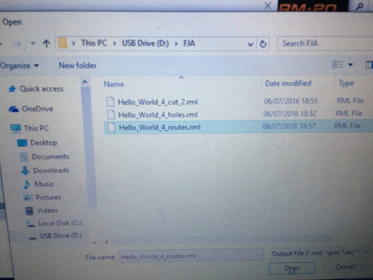
On the Rolandselecting file for the job
|
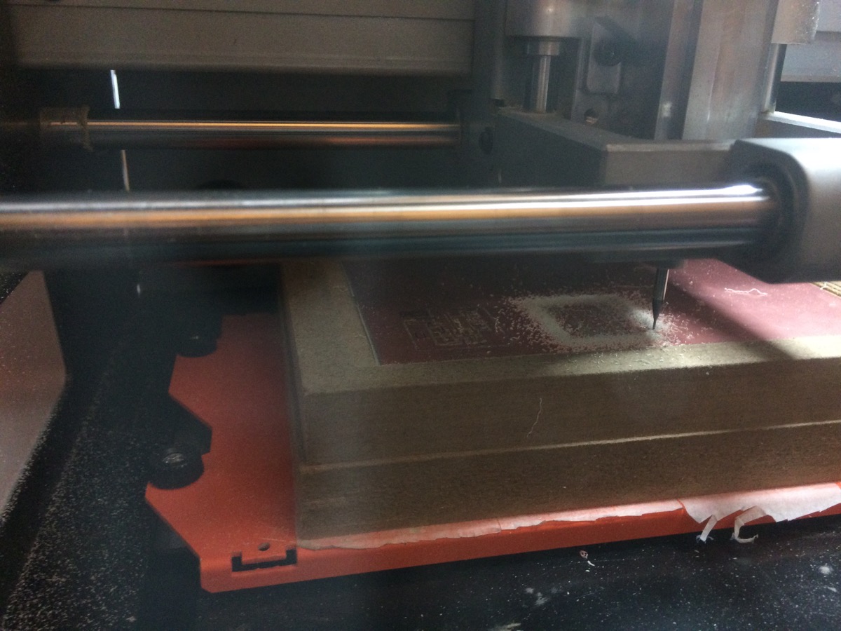
My friend Roland is milling ;-)
|
|
Boards milled, on the left the one with Error on 1 trace, on the right the final one
|
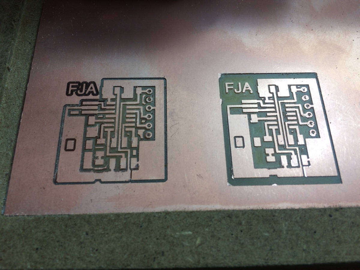
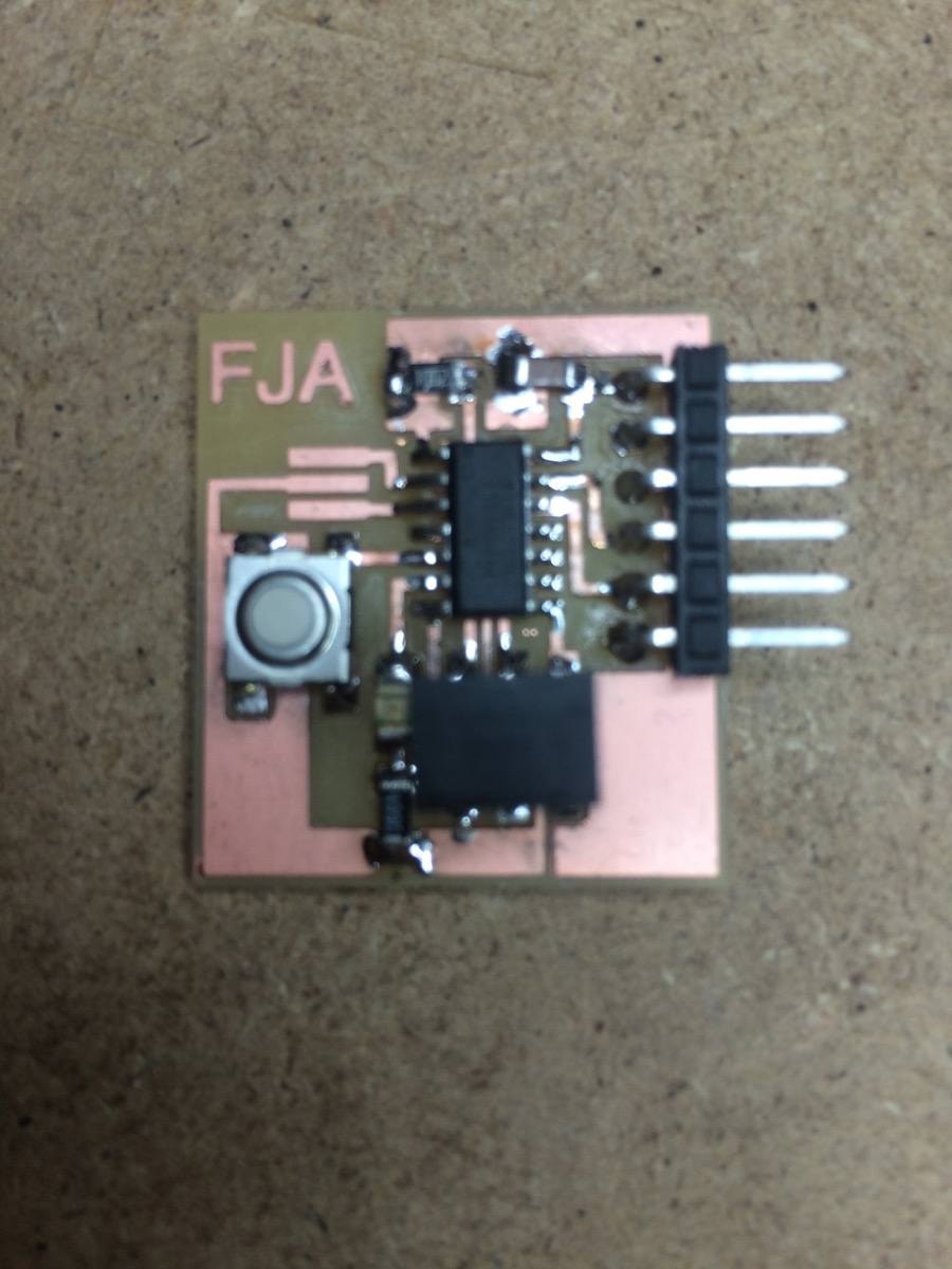
Here is the Final Version of my Hello-World Boardmore "aerated"
Milled and soldered version