Redraw the echo hello-world board
Our group,within this assignment, opted for Eagle as a design tool. In fact, it seems to be the most widely used open source electronic design software in the maker community. We left it up to everyone to eventually later test a different tool. I didn’t have any previous experience of this type of software so ,starting with Eagle, seemed to be a good solution. Andea Vial, a teammate with a strong background in electronics, gave us a lecture on both electronics and Eagle.
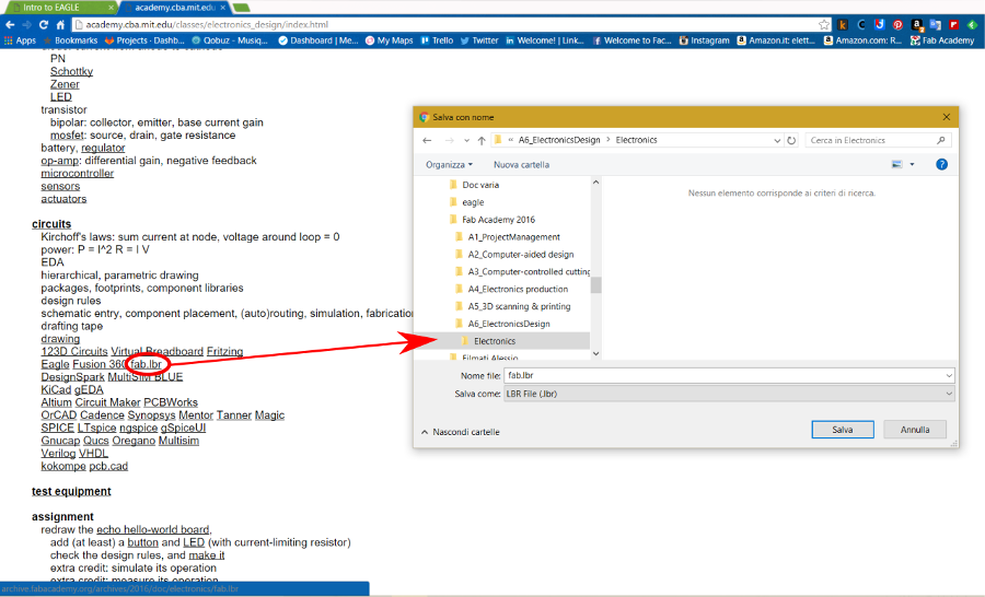
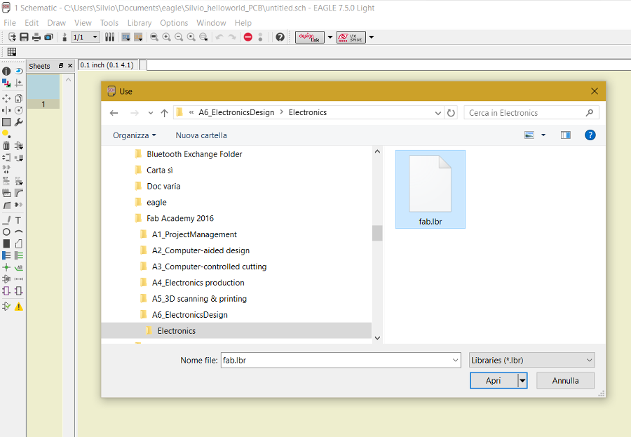
Following the assignment tutorial I downloaded the free version of Eagle. I then downloaded to a local directory the components library (fab.lbr) and uploaded it to Eagle using the “Use” command.
I then started to collect the different components from the library and gather them on the canvas, including the additional button and the led, and to connect them with lines using the “Net” command. I also used these lines to identify and name connection points not directly linked together. In this case the software prompted to confirm the connection. By the way, I did not find this software very intuitive to use (moving around and rotating components, labelling lines) but after the initial perplexity, I slowly began to feel more comfortable.
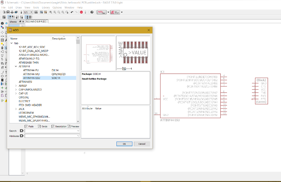
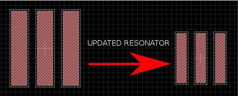
To account for the smaller traces of the resonator available in our Lab, I used a component specifically set up by Ernesto Voltaggio, a teammate. He created a new library named Volt.lbr which I uploaded in the system.
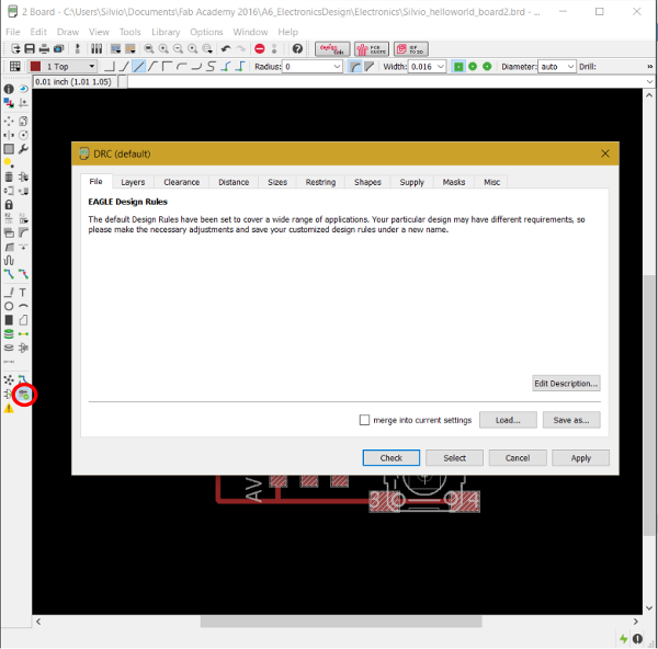
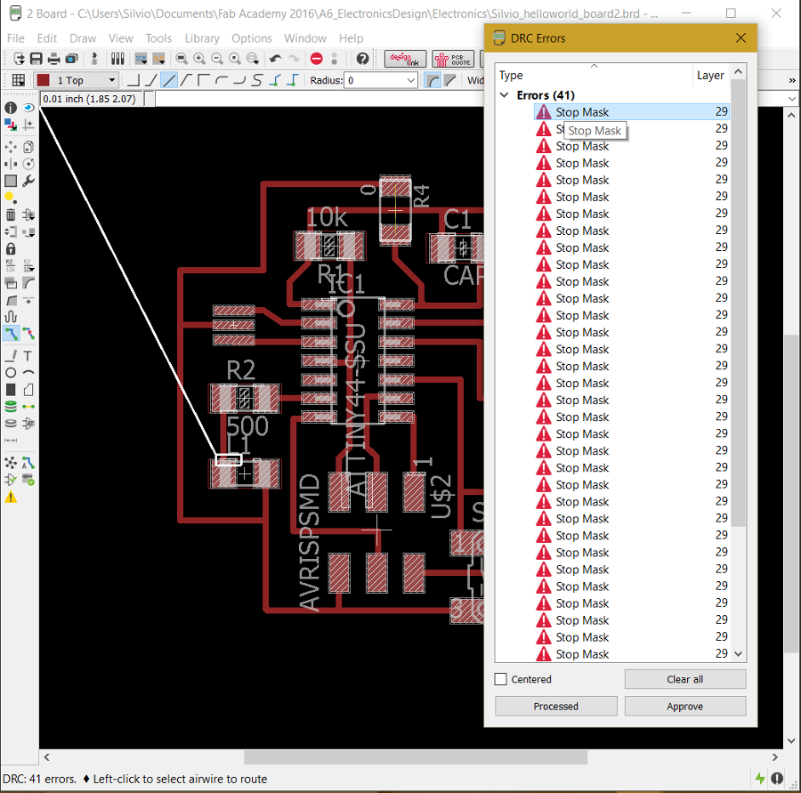
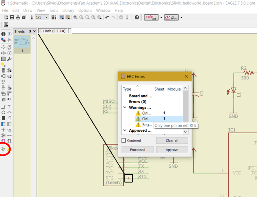
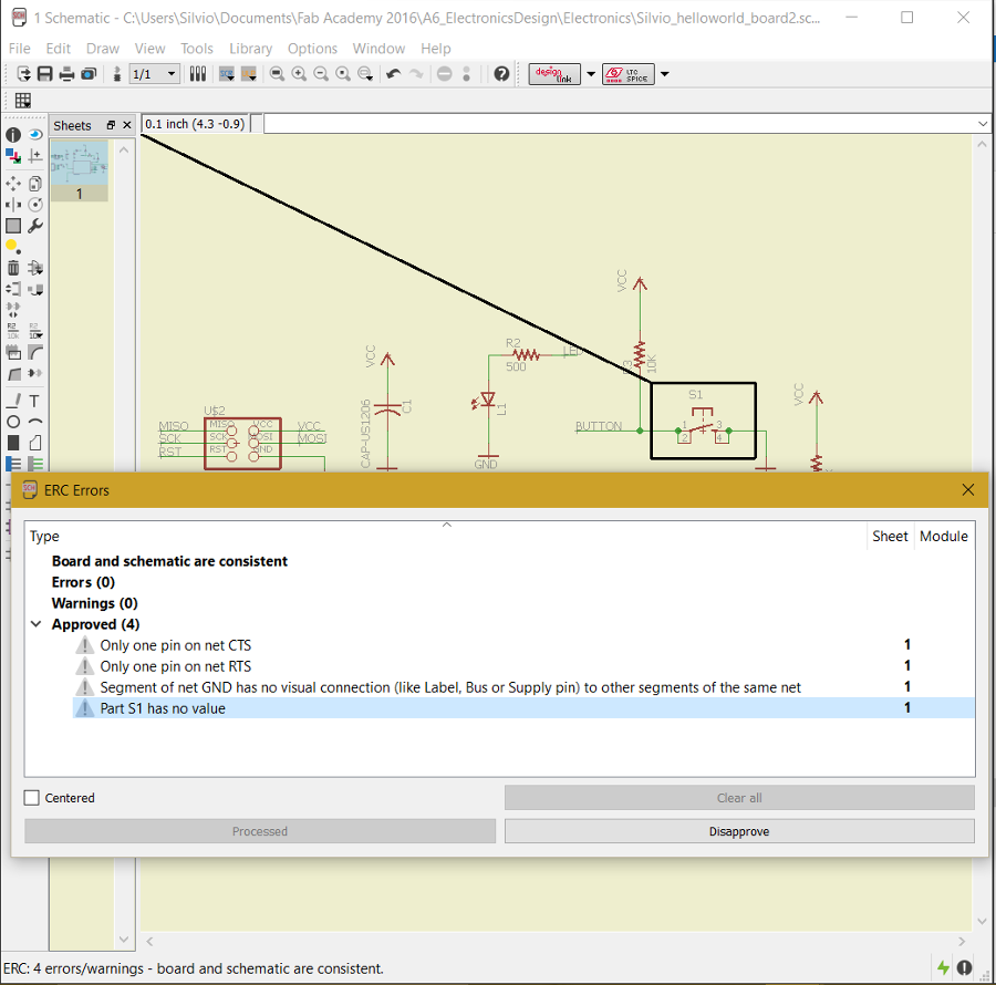
Once finished with the schematic, I checked the layout for mistakes with the ERC (Electrical Rule Check) command. I list of errors and warnings appeared mainly due to connecting lines overlapping the components . Some warnings simply needed acknowledgment, like “Only one pin on net RTS” or “Part S1 has no value” (the button).
Once the schematic was completed, I switched to the board view.
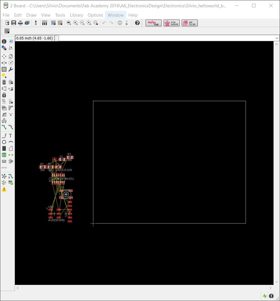
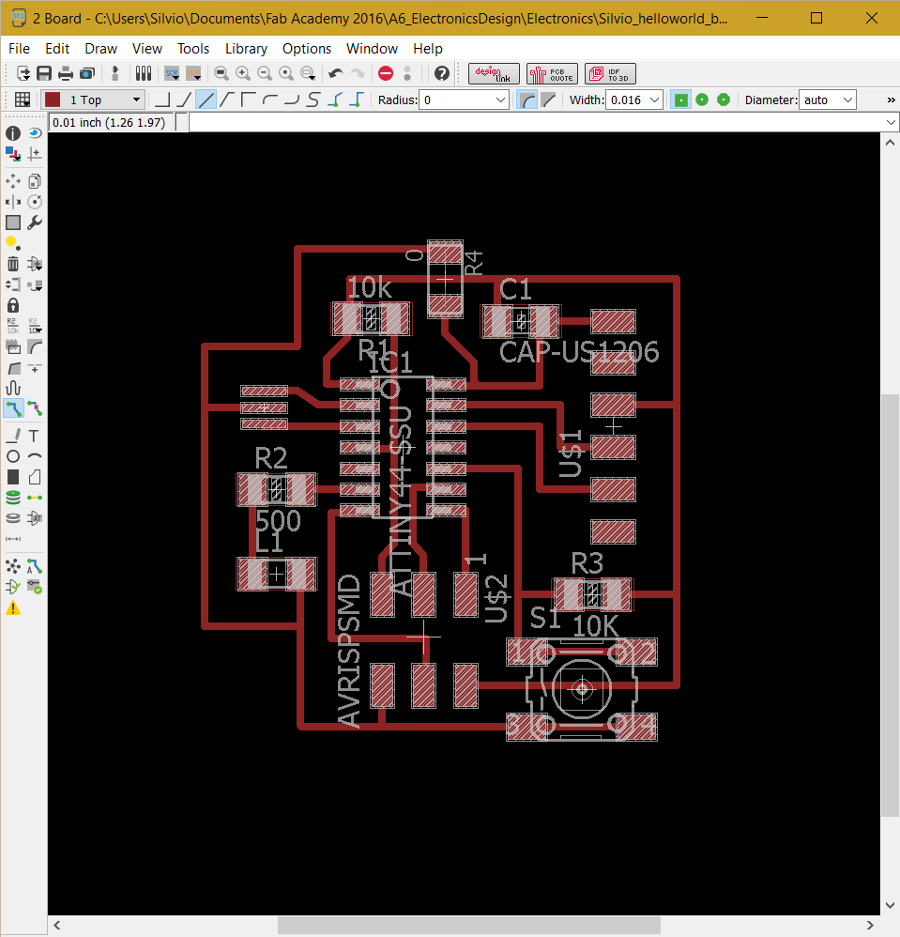
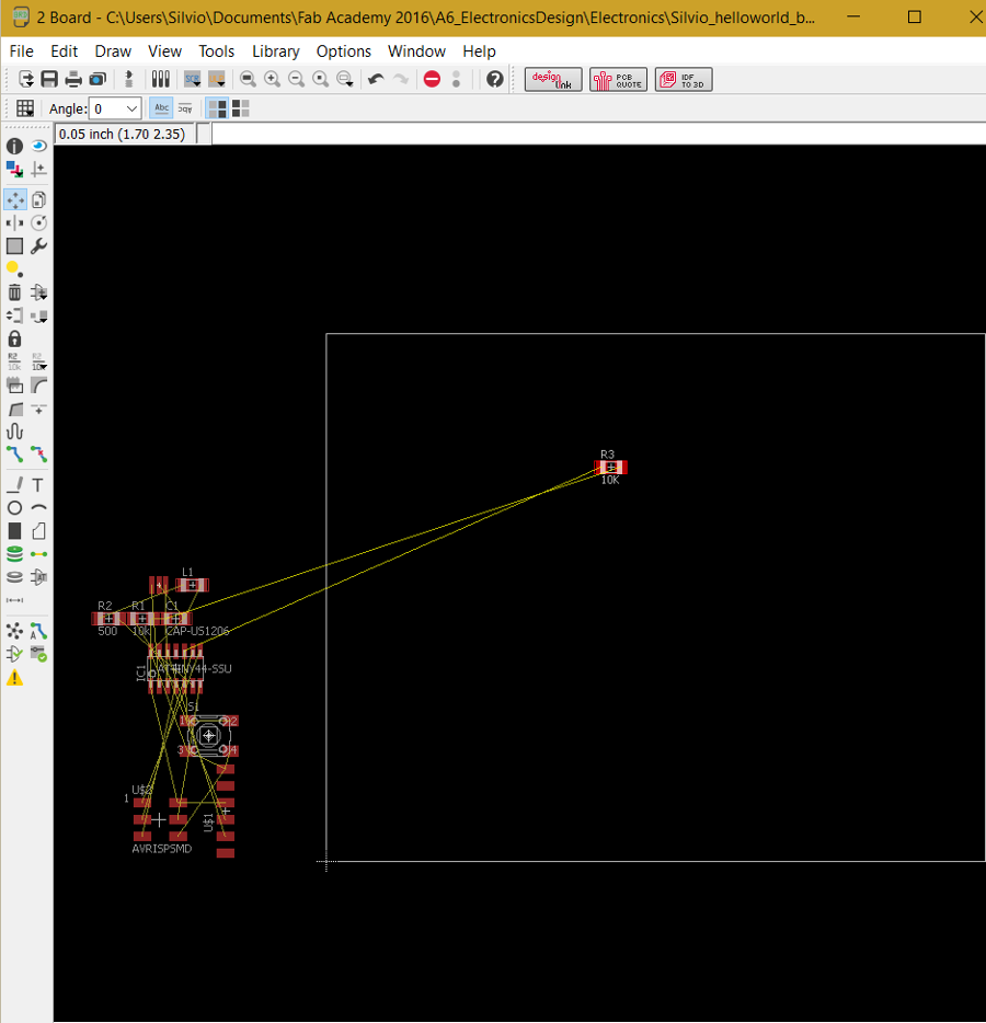
All the components were shown grouped together outside of the design area, connected with yellow lines. I moved a components at a time into the design area, matching the approximate location of the tutorial snapshot.
I selected the default width of the traces (0.016 mil) which made the routing comfortable. Nevertheless, this size did not allow drawing three traces under the microcontroller, like in the tutorial. So, instead of using thinner traces, I changed the routing and used a zero ohm resistance to bridge over a crossing trace. I first had to import the resistance into the schematic and make the necessary connections.
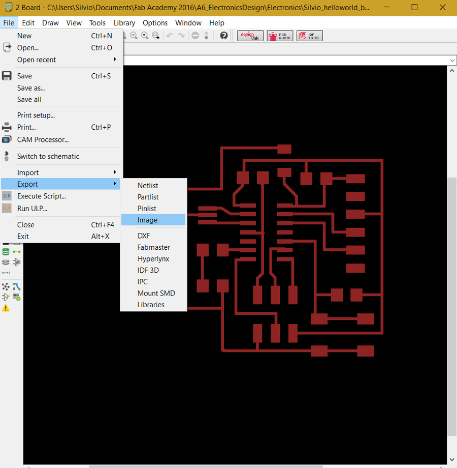
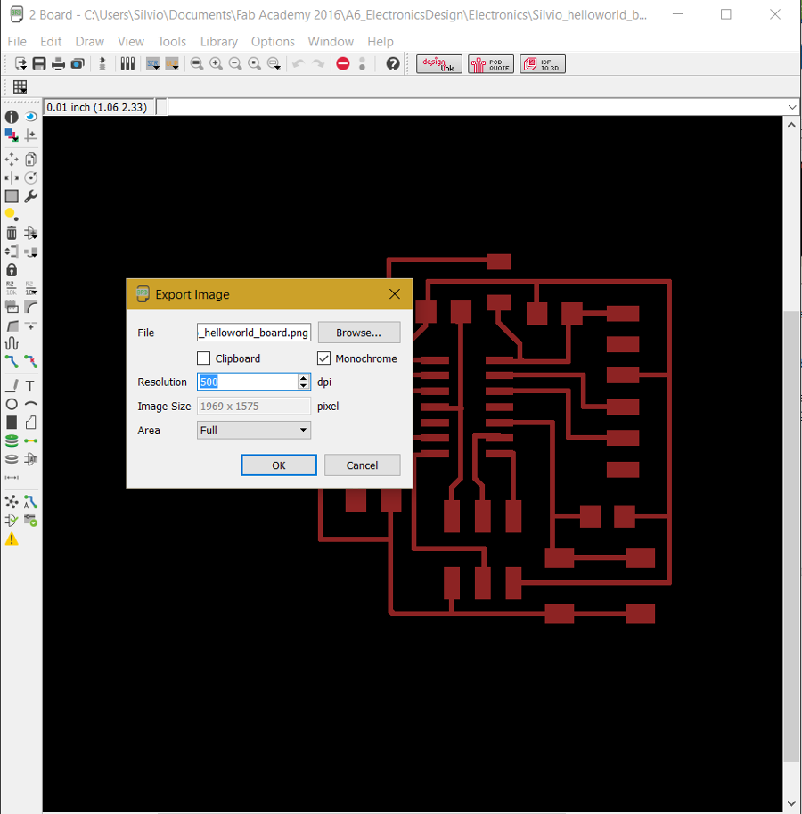
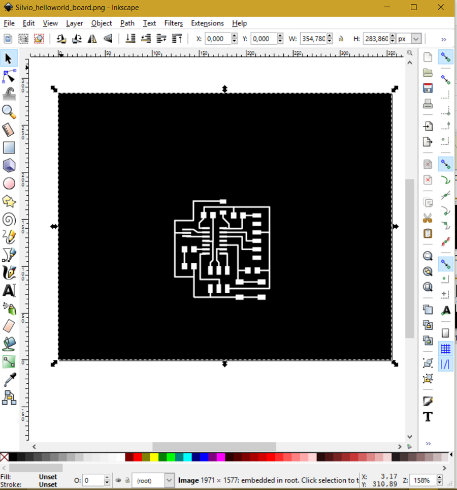
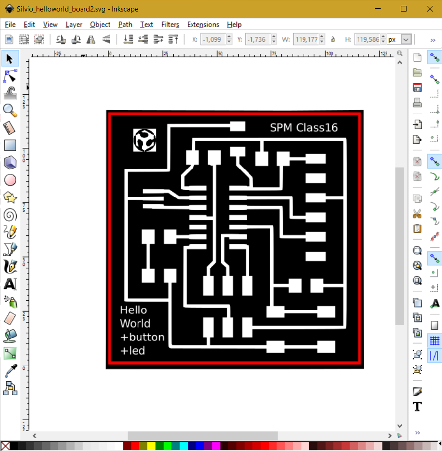
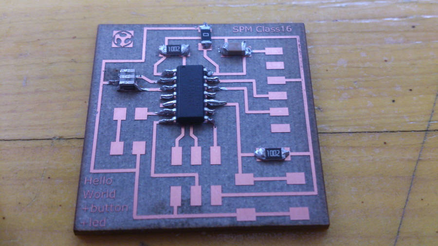
When you draw a trace between two pins connected with a yellow line, the system makes a confirmation sound and the yellow line disappears. Here is the final board (link to board, schematic).