Assignment
- Design and build a wired &/or wireless network connecting at least two processors.
- Demonstrate workflows used in network design and construction.
- Implement and interpret networking protocols.
- Described your design and fabrication process using words/images/screenshots.
- Explained the programming process/es you used.
- Outlined problems and how you fixed them.
- Included original design files and code.
Design and build a wired &/or wireless network connecting at least two processors
This week's assignment is to design and build a wireless network connecting at least two processors. I am planning to design a simple communication board using ATtiny45 Processor, one is transmitter and another one is receiver. The two board communicating using Radio Frequency(RF). My Project is Transmiter transmits one high signal to the RF Tx module which is transmitted using antenna. In the reciever portion the receiving antenna receives the Tx signal and passes to the processor, the processor decodes the data and controls an LED.
In this Project the data communication between the transmitter and receiver using the RF Tx & Rx module.
The RF module, as the name suggests, operates at Radio Frequency. The corresponding frequency range varies between 30 kHz & 300 GHz. In this RF system, the digital data is represented as variations in the amplitude of carrier wave. This kind of modulation is known as Amplitude Shift Keying (ASK).
Transmission through RF is better than IR (infrared) because of many reasons. Firstly, signals through RF can travel through larger distances making it suitable for long range applications. Also, while IR mostly operates in line-of-sight mode, RF signals can travel even when there is an obstruction between transmitter & receiver. Next, RF transmission is more strong and reliable than IR transmission. RF communication uses a specific frequency unlike IR signals which are affected by other IR emitting sources.
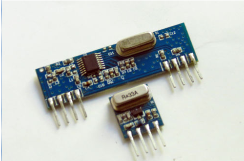
This RF module comprises of an RF Transmitter and an RF Receiver. The transmitter/receiver (Tx/Rx) pair operates at a frequency of 434 MHz. An RF transmitter receives serial data and transmits it wirelessly through RF through its antenna connected at pin4. The transmission occurs at the rate of 1Kbps - 10Kbps. The transmitted data is received by an RF receiver operating at the same frequency as that of the transmitter.
The RF module is often used along with a pair of encoder/decoder. The encoder is used for encoding parallel data for transmission feed while reception is decoded by a decoder. HT12E-HT12D, HT640-HT648, etc. are some commonly used encoder/decoder pair ICs.
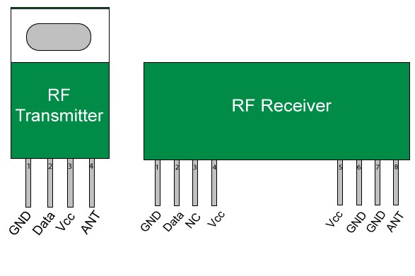
It's pinout is shown below
Features
- Range in open space(Standard Conditions) : 100 Meters
- RX Receiver Frequency : 433 MHz
- RX Typical Sensitivity : 105 Dbm
- RX Supply Current : 3.5 mA
- RX IF Frequency : 1MHz
- Low Power Consumption
- Easy For Application
- RX Operating Voltage : 5V
- TX Frequency Range : 433.92 MHz
- TX Supply Voltage : 3V ~ 6V
- TX Out Put Power : 4 ~ 12 Dbm
Applications
- Remote Controls
- Automation System
- Wireless Security System
- Sensor Reporting
- Car Security System
- Remote Keyless Entry
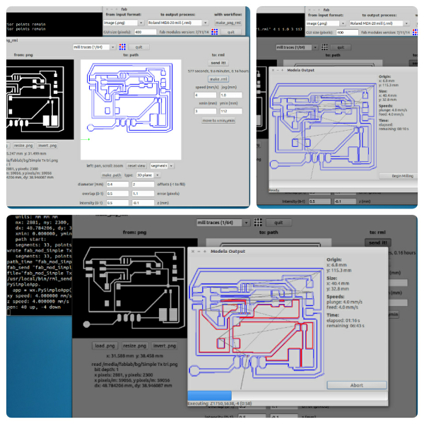
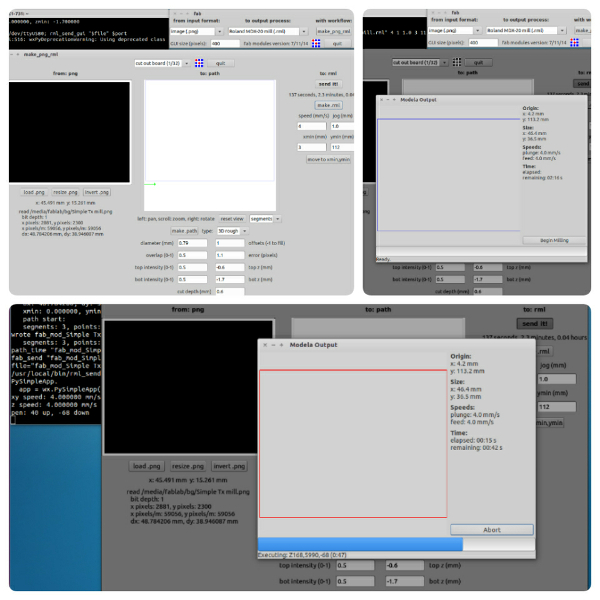
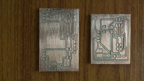
After completion of circuit design Mill and cut the PCB with milling machine. Setups are common as in the previous week.
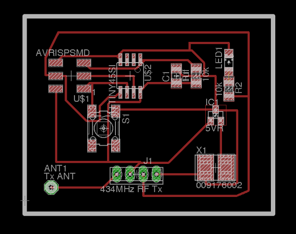
First I designed the circuit in Eagle software.
Transmitter
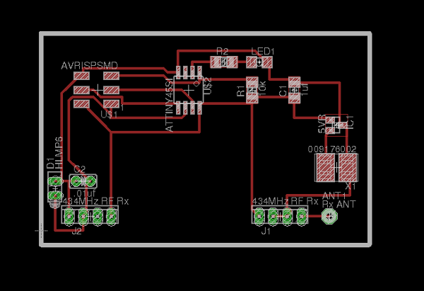
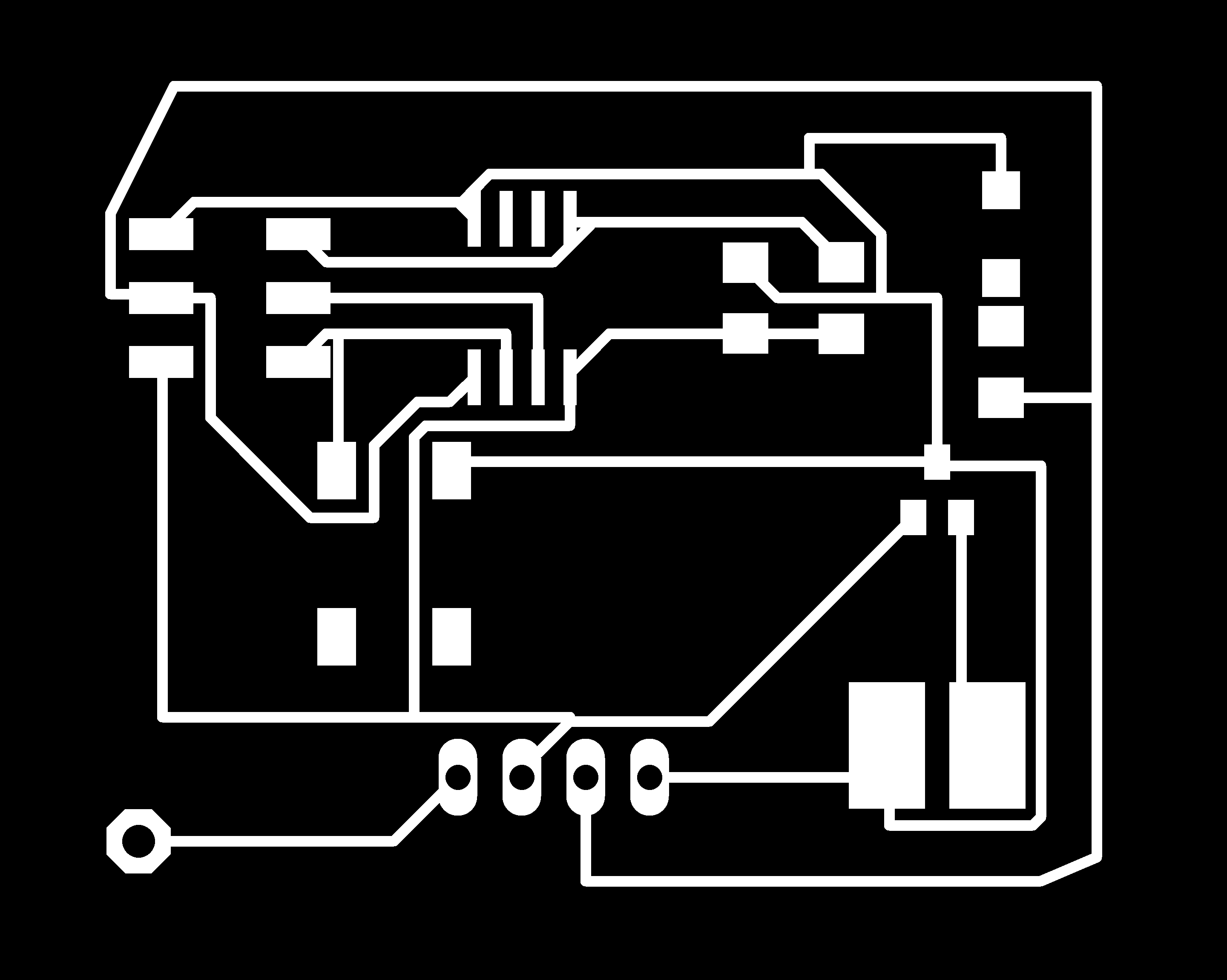
I designed ATtiny45 based simple Tx board, which contains ATtiny 45, ISP interface, Switch, RF434Mhz Tx module and Tx Antenna. My plan is to send a digital signal when I press the swich. First I design the circuit in eagle software. It contains ATtiny 45 one resistors, ISP connectors, switch, voltage regulators and Transmitter module. I designed it in Eagle and is shown below.
Receiver
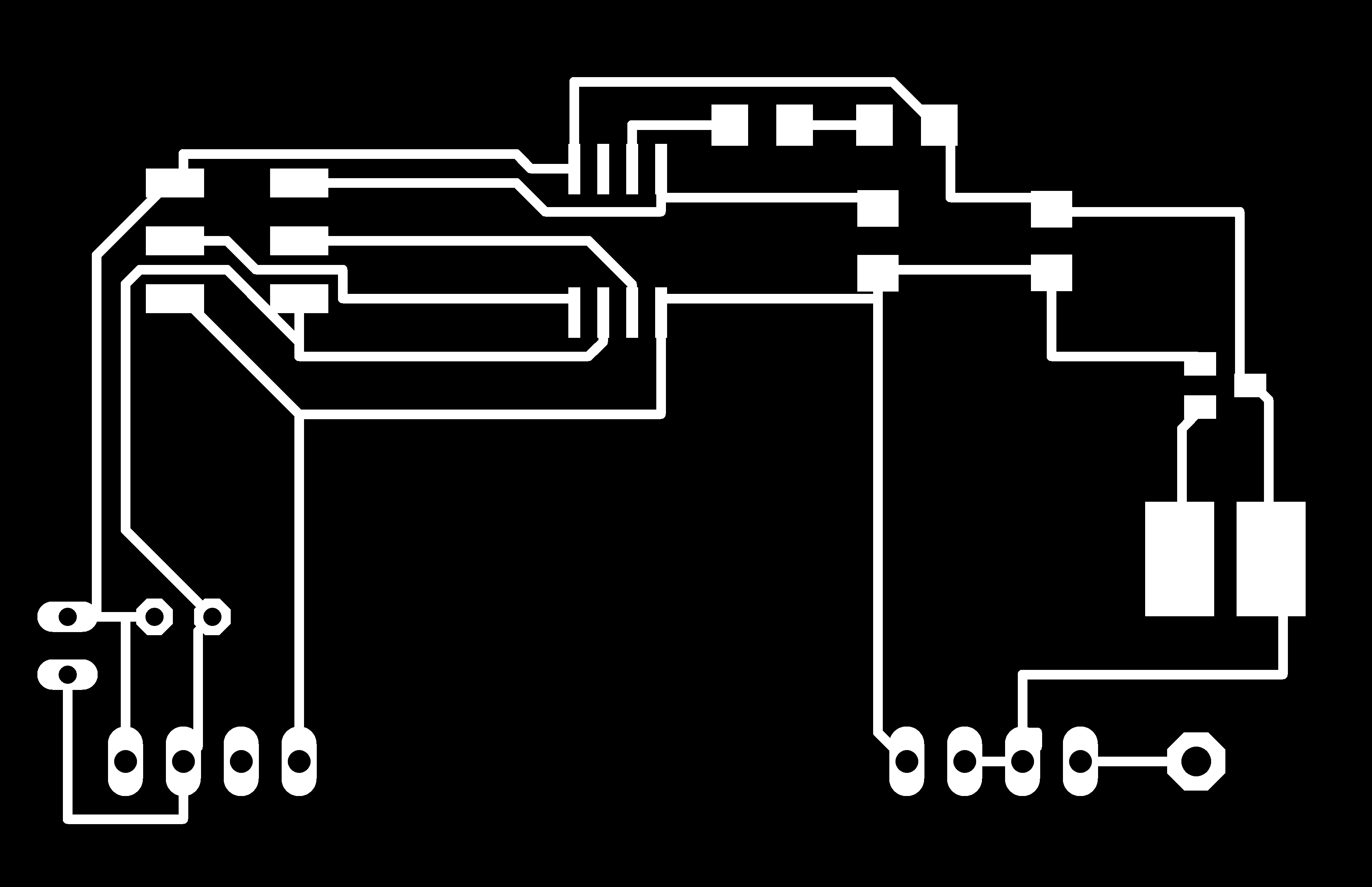
It contains ATtiny 45 one resistors, ISP connectors, voltage regulators, LED and Receiver module. I designed it in eagle and is shown below.
After completion of circuit design mill the board using milling machine
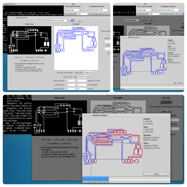
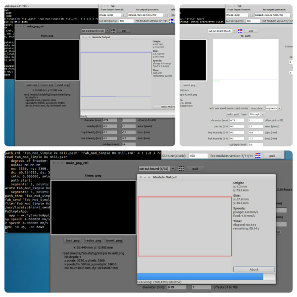
Tx & Rx PCB
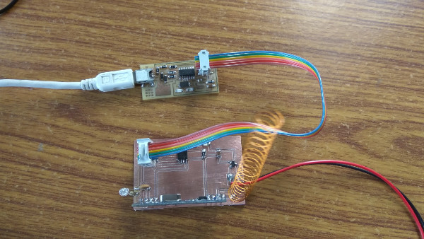
After milling the boards we need to solder the components to it so I refered the schematics of transimitter and receiver then soldered each component very carefully. The Tx and RX modules are soldered over the pads carefully.
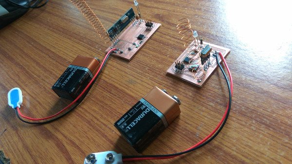
For Tx and Rx purpose I need an antenna. For that I made an helical antenna using the copper wire, which is available in the lab. A helical antenna is an antenna consisting of a conducting wire wound in the form of a helix. In most cases, helical antennas are mounted over a ground plane. The feed line is connected between the bottom of the helix and the ground plane. Helical antennas can operate in one of two principal modes — normal mode or axial mode.
In the normal mode or broadside helix, the dimensions of the helix (the diameter and the pitch) are small compared with the wavelength. The antenna acts similarly to an electrically short dipole or monopole, and the radiation pattern, similar to these antennas is omnidirectional, with maximum radiation at right angles to the helix axis. The radiation is linearly polarised parallel to the helix axis. These are used for compact antennas for portable and mobile two-way radios, and for UHF television broadcasting antennas.
In the axial mode or end-fire helix, the dimensions of the helix are comparable to a wavelength. The antenna functions as a directional antenna radiating a beam off the ends of the helix, along the antenna's axis. It radiates circularly polarised radio waves. These are used for satellite communication. You must choose an antenna for signal transmission. Usually, a 20-30 cm wire serves best. It is sufficient to give a range of 80 meters in open region. To improve the efficiency, you can also use a coiled wire (take a wire and make it into a coil). It increases the signal strength.
I made this antenna with the copper wire available in the lab, I coiled it like helix by rolling it over the marker pen.
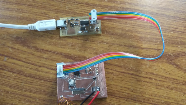
next is I have to burn the program in ATtiny45 processor in both the boards.
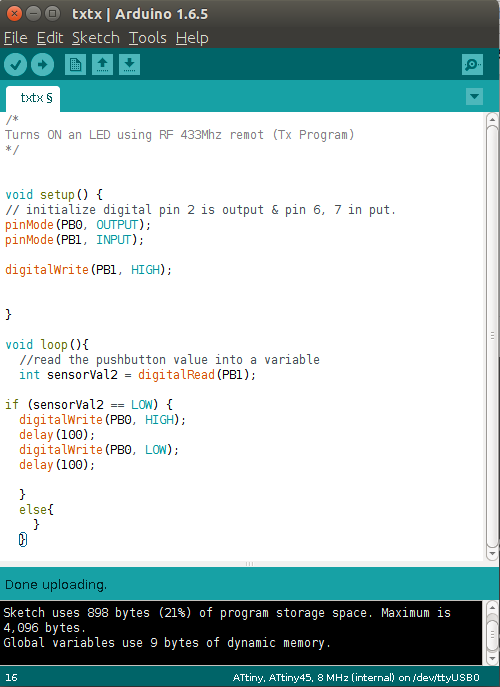
Transmitter program
I have written the code for Transmitting a pulse signal of 100ms duration.
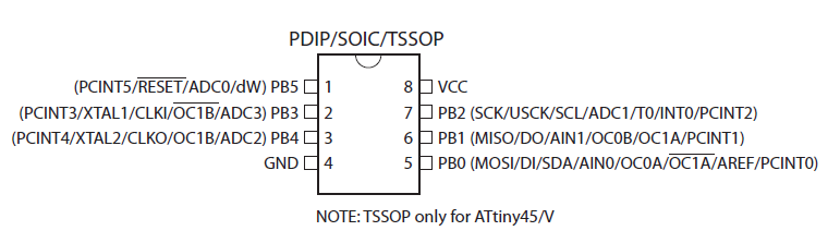
The program first initialize the I/O port of Attiny45. Here I am assigned PB0 as Output and PB1 as the Input you can see the pinout of ATtiny45 shown below. Next I set pin PB1 is HIGH for normal mode. When a switch is pressed (PB1 connected to GND with a push Switch) PB1 gose to a LOW state this will read through PB1 port of ATtiny45. When a Low state recieved, the output port will be high for 100ms, for this I given a delay of 100ms after that it will goes to a low state. So it will give a pulse of 100ms duration and is converted into the RF signals by RF TX module and is transmitted through the antenna. The program is also shown below.
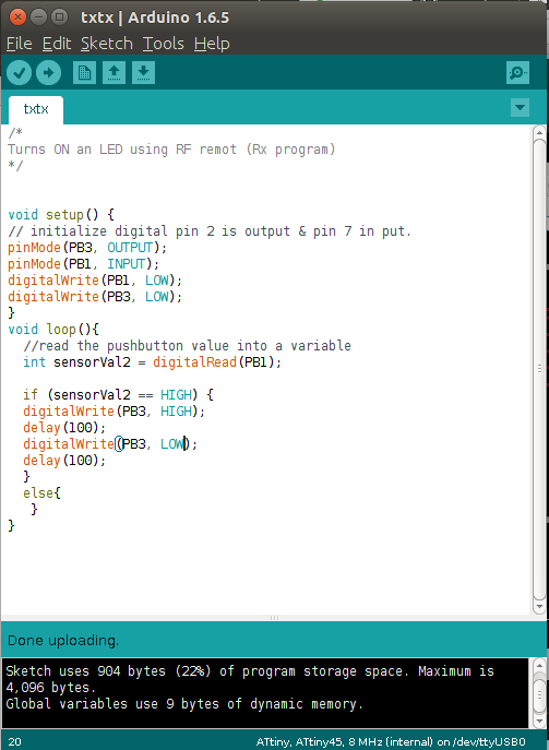
Receiver program
I have writen the code for Reciving the signal which is Transmitted from the Tx board. Here the processor checks for a high input in its PB1 pin. When a High is recieved the LED in the out put(PB3) is ON.
In this part first initialize the I/O port of Attiny45. This is the receiver part so we have to receive the data transmitted by the antenna. Here I am assigned PB3 as Output port and PB1 as Input, I initialised PB1 as LOW state for the Normal mode. Next the program will continuosly scan the data of PB1,once a HIGH is received the port PB3 will be set to HIGH with a delay of 100ms after that it will be turned LOW. The programm is shown below.
OutPut is like:
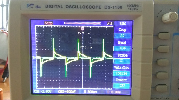
In order to test this circuit connect the 9V battery to the board using battery snaps and once the board is turned ON we can test it by just push the switch it will send the pulse through the antenna and if look at the Receiver side the output of the receiver is an LED, it will glow according to the pulse signal. The output also observed on the DSO.
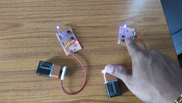
During the testing I observed that some false triggering is happening in the Rx board. On further analysis we found that some noise picking is happening in the receiver section this is the main issue. Inoreder to avoid that we put a capacitor of value .02uf between the reciever input and GND. This time the error didn't happen and the problem is getting redused. I also verified the input and output signal in the DSO.
Download My Design files
Transmitter milling PCB PNG file
Transmitter cutting PCB PNG file