Exercise 04 - Electronics Production
Assignment
Our assignment for this week is to build the FabISP In-circuit Serial Programmer for the AVR series of MCUs. We were told that we could make the ISP using either of Neil's, David Mellis', Andy's, Valentin's or Zaerck's design.
There are actually a few things that we have to do for the assignment this week:
- 1. Make the FabISP pcb
- 2. Stuff the board and solder the components
- 3. Program the firmware onto the FabISP board
- 4. Test the board
Step 1: Making the FabISP Board
We have a number of options for making the FabISP board. I've decided to work with Neil's FabISP board, as I have made it before and I like the idea of a fixed USB connector as compared to PCB-finger connector. I've found that the pcb-finger connectors, at least for my self made boards, are generally a bit loose and may result in connection issues.
I have a few options for making Neil's FabISP board, viz:
- importing the png traces and outline file into fab modules and generating gcode for our China pcb milling machine
- using Eagle CAD to read the png traces and board outline and generating gerber files for our LKPF pcb milling machine
- using Eagle CAD to read the png traces and board outline and generating gcode for our China pcb milling machine
- redrawing the entire FabISP circuit in Eagle and generating the files for pcb milling
- using the FabISP circuit in Kokopelli's examples folder to make the pcb
To familiarise myself with the various workflows, I've decided to both use Fab Modules and Eagle CAD to generate the files required for pcb milling. We have an MDX-540, but no MDX-20 or SRM-20 in our Fablab. We are in the process of purchasing additional desktop 2.5D routers for pcb milling, but at the moment, our options are either to generate files for our LKPF or China pcb milling machine. We also have an iModela, which is compatible with Fab Modules, but my personal experience with the iModela is that the machine lacks the precision to mill pcbs that we will need further down the road. Both the LKPF and th China PCB2020B are much better machines.
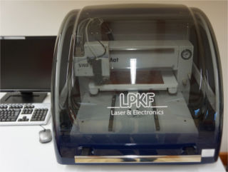
The LKPF Protomat S103 is a high-end, dedicated pcb milling machine with automatic tool changer (ATC). It is a fantastic machine - when it works. However, the S103 can only be used with LKPF's Circuit Pro software and this software only accepts gerber files, so going from Fab Modules to the S103 directly is not possible. I would need to import the png files from Fab Modules to Eagle CAD, then use Eagle CAD to generate the gerber files for the S103.
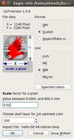
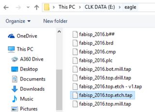
To generate gerber files from the FabISP png files, they must first be imported into Eagle CAD. Start Eagle and create a new project at the Eagle Control Panel. I've called my new project FabISP_2016. In the empty project, create a new board, FabISP.
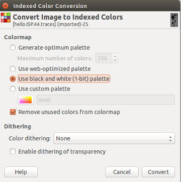
Eagle can import a number of file types, including bitmap, gerber, dxf, pcad, protel and altium. Sine the FabISP files are in png, I first reduced them to 2 color BW and converted them to bmp in GIMP. I also checked the scale factor for the original files using Inkscape:
- hello.ISP.44.interior: 1149 x 2260 px or 22.987 x 45.214 mm
- hello.ISP.44.traces: 1149 x 2260 px or 22.987 x 45.214 mm
To reduce the png file to 2-color BW, I used the Image/Mode/Indexed... option in GIMP and selected "Use black and white (1-bit) palette", followed by convert. I then exported the results as a bmp image file. Note: I inverted the hello.ISP.44.outline image so that the board outline was white before exporting the bitmap.
After the png files have been converted to 2-color bitmap images, they have to be imported into Eagle. This is done using the File/Import/bmp menu selection. For the hello.ISP.44.interior file, I imported the black pixels into Eagle layer 20, the dimension layer. For the hello.ISP.44.traces file, I imported the white pixels into Eagle layer 1, the top layer.
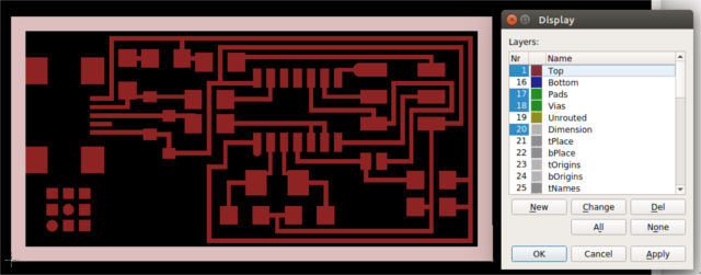
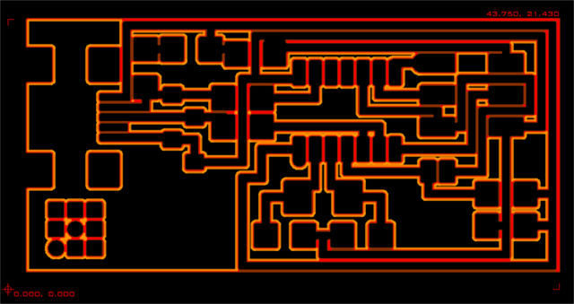
The final FabISP board in Eagle is shown below, after turning off unnecessary board layers and rotating the image. Note: You need to keep one corner of the board at the origin, as all gerber/gcode is computed from that point.
Eagle to Gerber
To create the gerber files for the LKPF S103, select File/CAM Processor... in Eagle. Once the CAM Processor dialog box opens, select File/Open/Job and select gerb274x.cam as the job. The dialog box changes to show the different layers of gerber files produced: component, solder, silk screen, solder stop mask (CMP) and solder stop mask (SOL). For the FabISP board, we are only interested in 2 of the layers, component and silkscreen.
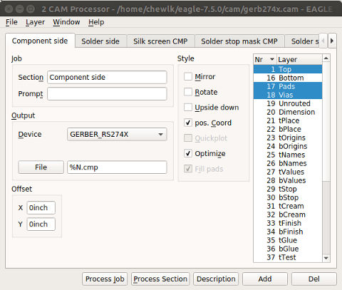
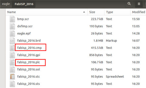
For the component side tab, make sure that only the top, pads and vias layers are selected. For the Silkscreen tab, make sure that only the dimension layer is selected, as we do not want any component names to appear on the board outline. Component gerber files have a .cmp file extension and silkscreen gerber files have a .plc file extension. Click "Process job" to create the gerber files, then close the CAM Processor dialog box. The gerber files are located in your project directory.
Eagle to GCode
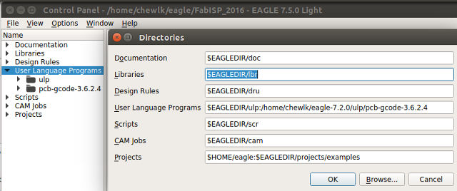
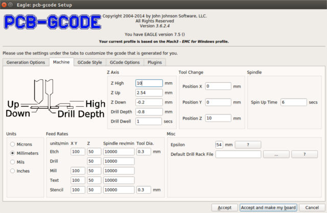
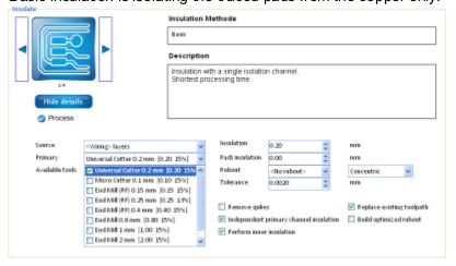
To generate GCode from Eagle, you need to add the PCB-gcode plugin. This can be downloaded from the PCBGCODE.ORG site. After the file has been downloaded, unzip it and copy it to the Eagle/ulp folder. Go to the Eagle Control Panel. Select Options/Directories and add the path for the pcbgcode folder to the User Language Programs section. Click OK and verify that pcbgcode ULP has been added to the program.
To generate gcode for the trace layer, turn off the dimension layer, so that only the trace layer is showing. Select File/Run ULP, then select pcb-gcode-setup.ulp. The first time that you run pcb-gcode, you need to configure the settings for your system. The 3 main options to set are in the Generation Options, Machine and GCode Style tabs.
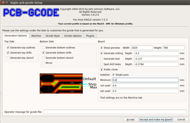
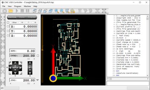
The figure below shows the pcbgcode viewer simulation for a multi-pass isolation mill of my FabISP board, with the following:
- Tool diameter: 0.2mm
- Milling depth: -0.2mm
- Minimum isolation: 0.1mm
- Maximum isolation: 0.2mm
- Step size: 0.05mm
Some useful links for learning Eagle CAD:
PNG to GCode: FabModules
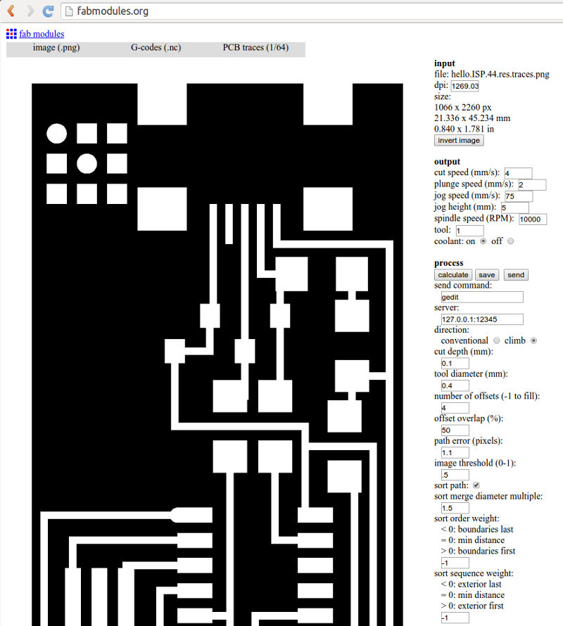
Fab Modules provides another workflow for moving from our board design on the computer to the physical pcb. Fab Modules is available as both a compiled version, downloadable from Kokompe.cba.mit.edu, as well as an online version at fabmodules.org. We start with the traces png file from Neil's fabisp board.
- 1. Go to Fabmodules.org.
- 2. Click on input and select the traces png file.
- 3. Click on output and select G-codes (.nc)
- 4. Click on process and select PCB traces (1/64)
- 5. On the right of the browser window, adjust the cut parameters for the machine.
- 6. Click the calculate button to generate the toolpath.
- 7. Click the save button to save the generated gcode.
- 8. The gcode can now be sent to the pcb-milling machine to cut the pcb.
- 9. Repeat the sequence for the board outline png, using PCB outline (1/32) as the process.
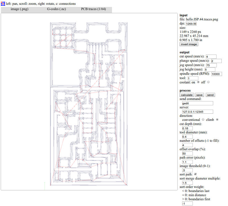
For the FabISP traces, milling on our PCB2020B, I used the following parameters for the nc file:
- Cut speed: 4 mm/s
- Plunge speed: 2 mm/s
- Cut depth: 0.18 mm
- Tool diameter: 0.4 mm
- Number of offsets: 4
- Offset overlap: 50%
For the FabISP board outline, milling on our PCB2020B, I used the following parameters for the nc file:
- Cut speed: 4 mm/s
- Plunge speed: 2 mm/s
- Cut depth: 0.6 mm
- Stock thickness: 1.7 mm
- Tool diameter: 0.79 mm
- Number of offsets: 1
- Offset overlap: 50%
My PCB design files are in the links below:
Milling the PCB
I've tried 3 different approaches to milling the pcb:
- Using the LKPF Protomat S103
- Using the iModela
- Using the PCB2020B
The workflow involved in each of these methods is slightly different, with the iModela and PCB2020B approach being closest to fabmodules. The LKPF S103 is essentially a proprietary, closed source system and requires the use of it's own software, CircuitPro.
LKPF Protomat S103
CircuitPro is Windows only software, available as a free download if you are an LKPF customer. The software requires the notebook to be hooked up to the S103 via 2 usb connectors, in order for it to work. LKPF has tried to make the entire pcb milling process menu driven.
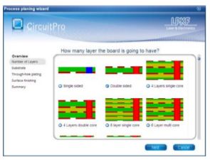
To start, launch CircuitPro by double-clicking on the program icon on the Windows desktop, then click on the "Execute Process Planning Wizard".

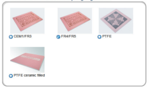
Select the template based on the board that we will be cutting. Most of the pcbs that we will make during the Fab Academy course are single-sided PCBs with traces milled on the component-side. Select the type of material. LKPF recommends FR4, but we actually make use of FR1 stock instead of FR4, as it is more environmentally friendly. The board is also mounted onto the base platform at this time. Verify the configuration and click "Done".
The next step is to import the gerber files that I generated earlier into CircuitPro. 2 files need to be imported, the top etch (.cmp) and the board outline (.plc). Change the layers/template column to match the layers that we are importing the files to and press "OK".
For this board, we do not need any rubout areas nor fiducials, so we can go straight to creating the tool pathways. I have selecte isolation milling, as there is no need to remove all the unwanted copper around the traces.
The last few steps in the process would be to set the 0,0 coordinate for the mill-bit and to position my pcb-layout on the bare copper. This process is not very user friendly in the S103 and I prefer the iModela/PCB2020B approach, which allows me to position the 0,0 (Home) position a lot easier and more accurately.
Once the board and milling head has been positioned, milling can begin. One advantage of using the LKPF S103 is that it comes with an automated tool changer, so switching between bits for milling the traces and cutting out the board outline is a lot more convenient. If, a very big if, all goes well, the we end up with a perfectly milled pcb. I'm not overly fond of the S103, as I find that it is very temperamental and too many things can and does go wrong, in my experience. Once the system acts up, we basically need to call in the vendor to re-tune the machine.
PCB 2020B
The PCB 2020B is a cheap DIY pcb-milling machine that I bought from China last year for USD400, inclusive of S&H, for our Fab Academy course, as the LKPF S103 gave us a lot of frustration and unreliable results and the iModela was too light-weight to mill pcbs in the volume that we needed.
The PCB2020B machine is a Mach-3 compatible milling machine. The USB-control board is USBCNC compatible and interfaces between the PC and the Mach-3 controller board. The input for the PCB2020B is a gcode file, which can be from fabmodules, or generated from Eagle, using the pcb-gcode ULP. Since I already had the FabISP artwork imported into Eagle, I used pcb-gcode to generate my cutfiles for the PCB2020B.
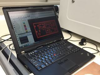
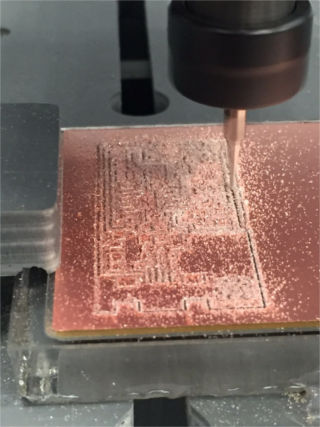
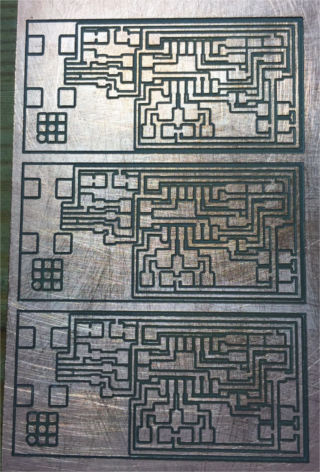
The USB CNC Controller software is really very user friendly. The loaded gcode file is displayed as a graphic in the program and this image is updated as the traces is being milled, so that the user can follow the progress of the milling operation. After positioning the mill-bit at my designated Home location (XYZ 0,0,0 coordinates), I clicked on the "PLAY" button to mill the board. Here, I've rotated the FabISP board in Eagle, so that I can mill up to 3 boards onto a single 3"x2" FR1 pcb stock.
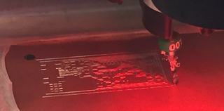
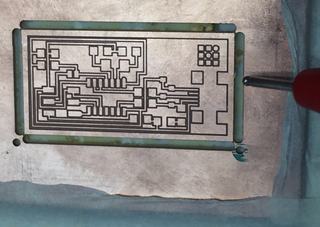
The pictures below show my FabISP board being milled and the pcb after washing and cleaning.
Stuffing & Soldering
Before stuffing and soldering the board, it is VERY important that the board be checked for continuity and to make sure that there are no shorts. I've found that most of the problems with my fabricated PCBs are usually due to open or short circuits in the PCBs, for example, due to taces of copper being left behind after the milling process.
I've found stuffing and soldering the PCB to be a very straight forward and simple process. I only need to take my time, be meticulous and not rush through the process, and to ensure that all my solder joints are good. My almost completed FabISP pcb, which is short of a zener diode, is shown in the picture below. It took me about 45 minutes to find and organise my components and to solder the pcb.
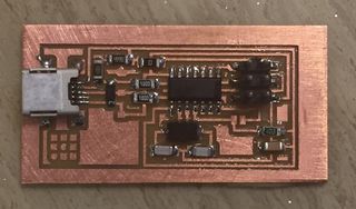
I've stuffed and soldered the last zener onto my pcb. I then checked the board for continuity with a multimeter, making sure that all my connections were good, according to the schematic diagram. My FabISP board is now ready for programming. I will need to short the SJ1 (program) and SJ2 (power) jumpers for the programmng stage. I've decided to short the SJ2 jumper permanently with a zero ohm resistor, so that my FabISP board can supply power to my target boards.
Programming the Firmware
There are 2 parts to programming the firmware onto the FabISP board.
- 1. Installing the programming software, e.g. avrdude
- 2. Downloading the firmware and creating the FabISP hex file.
The FabISP firmware is based on the USBtiny and V-USB firmwares. The original FabISP design was done by David Mellis at MIT and there are many versions of the design available now. The firmware for Neil's FabISP design is based on the ATTiny44 MCU. If a different MCU, such as the ATTiny45 or ATTiny85 is used, then the sourcecode must be modified and the firmware must be recompiled.
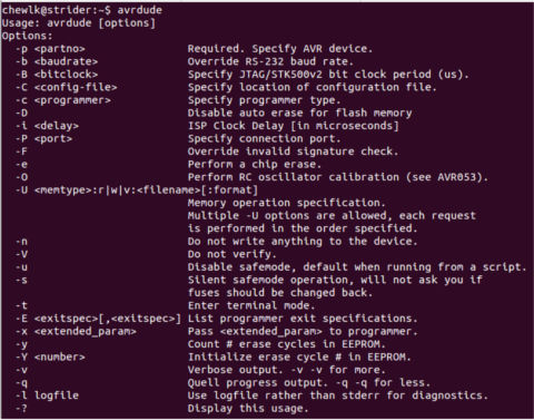
AVRDude is available for Linux, OSX and Windows and I have tested programming the FabISP across all 3 platforms. To install avrdude on Ubuntu, the steps are:
    sudo add-apt-repository ppa:pmjdebruijn/avrdude-release
    sudo apt-get update
    sudo apt-get install avrdude
On Windows, the corresponding steps are:
    Download WinAVR package from sourceforge
    Install the software
    Open a command window, type avrdude
I next downloaded the FabISP firmware and unzipped it to my Desktop. Looking through the folder, there is already a main.hex file. I decided to re-compile the firmware for my programmer.
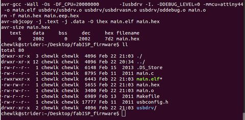
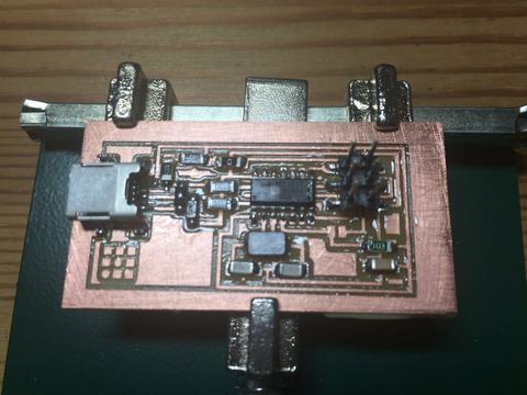
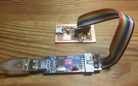
There are many ways to program the FabISP. You could use another FabISP, a commercial ISP programmer, or even an Arduino board. For this exercise, I decided to use a USBASP v2.0 that I had. After connecting the USBASP to my FabISP board via the 6-way IDC header, I was ready to take the next step. The Makefile must be modified for the type of programmer that you are using.
The procedure to follow is:
      make clean
    make hex
    make fuse
    make program
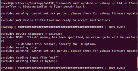
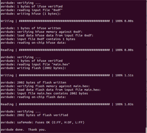
Looking through the Makefile, the programming for my FabISP is via the following avrdude command:
avrdude -c usbasp -p t44 -U lfuse:w:0xff:m -U hfuse:w:0xdf:m -U flash:w:main.hex:i
I have basically instructed avrdude to program my FabISP using the USBASP programmer, for the ATTiny44 MCU on the FabISP, with lfuse value of 0xff (ext osc, SPI enabled) and hfuse value of 0xdf and the firmware main.hex.
Avrdude reported the entire programming process and my FabISP board is now ready to be used as a programmer.
FabISP Referencees:
- FabAcademy Electronics Production tutorial
- FabAcademy FabISP Programming tutorial
- AVR Fuse Calculator link
- Avrdude Tutorial
- Arduino as ISP using avrdude
Testing the FabISP
My next goal is to mill and stuff the Fab Academy Hello board and program this board using the FabISP that I have made. However, due to the constraints of time, that is left for another day.