06.ELECTRONICS DESIGN
Mar 3, 2016
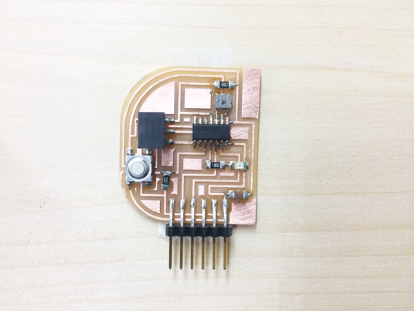
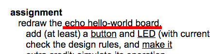
This week I made an echo hello-world board. The assignment is redraw it. And add (at least) a button and LED (with current-limiting resistor), check the design rules, and make it.
But it was too difficult for me...;( So,I will work hard at practice.
[Tool]
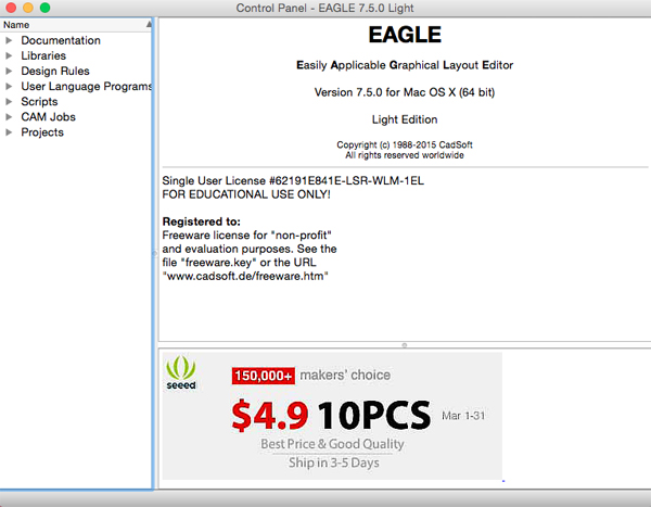
Software :Eagle (MacOSX) > Fabmodule (ubuntu)
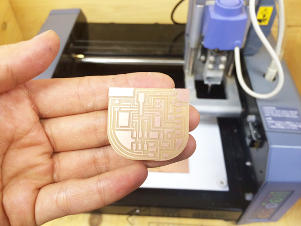
CNC Milling machine : Roland MODELA MDX-20
[Data]
Schematic data: test_2_160309.sch
Board data: test_2_160309.brd
04-1. Eagle setup

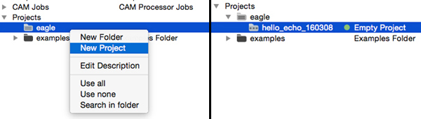
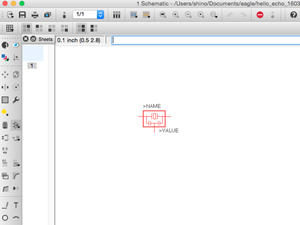
04-2. Schematic design
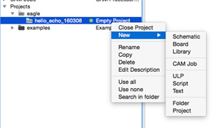
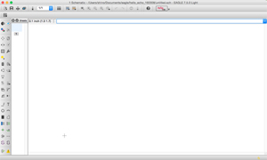
Open the window of new schematic design.
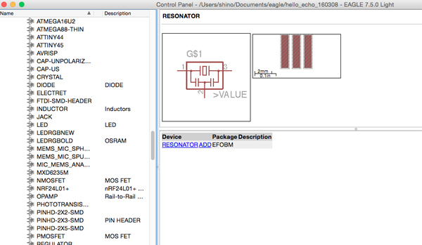
In this assignment, I used these components.
[Components]
- Attiny44
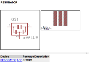
- 20MHz Resonater
- 1uf Capacitor
- 100 Resistor
- 10k Resistors
- Led
- Tactile Switch
- 6 Pin SMD Type Male Headers
- 6 Pin Right Angle Male Header
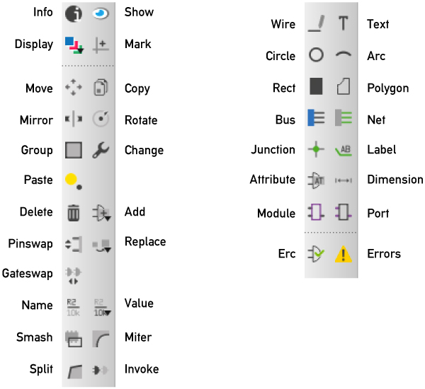
- Show: Show names and other details of objects and objects
- Display: It is often easier to maintain a good overview if some information is not shown.
- Move: Move for instance wires (lines or signal tracks).
- Delete: Delete objects with this command.
- Wire: Draw lines.
- Text: With the TEXT command you place the texts.
- Arc: Draw arcs.
- Junction: Draw intersection.
- Label: Rename components.
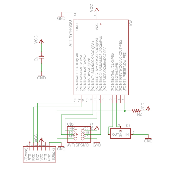
( Schematic data > test_2_160309.sch )
04-3. Board Design
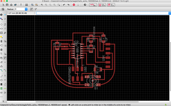
I was particular about designing without jumper wire.
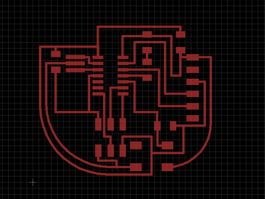
I saved each data as png data.
The detailed records are as follows.
Photos > [FabAcademy2016] Week06
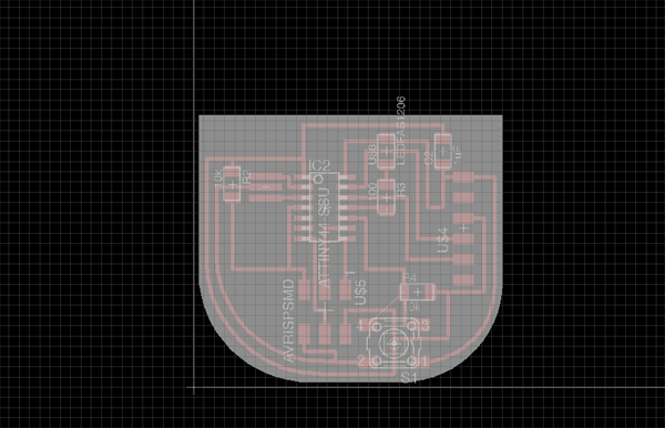
04-4. Assemble
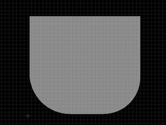
The data I used are these.Data > cutout: work06_160309_cutout.png, trace: work06_160309_trace.png
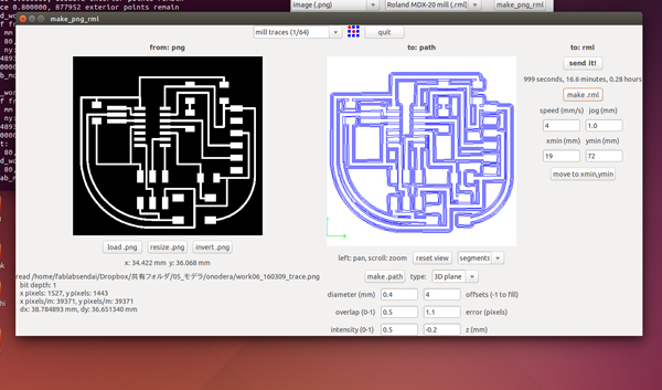
And paths are displayed when you set "offsets" for "-1" and click "make .path". (※"Offsets" is set-point of the line which the end mill paths on. It is usually "-1".)