Assignment 6: Electronics Design
I used Eagle for the electronics design. At first I dowloaded the fab.lbr
component library and copied the file to the Eagle installation
library C:\EAGLE-7.5.0\lbr.
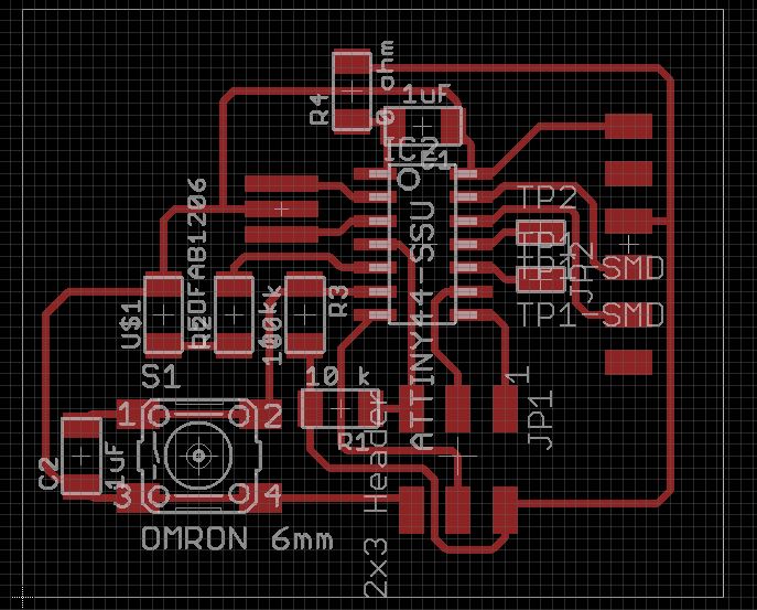
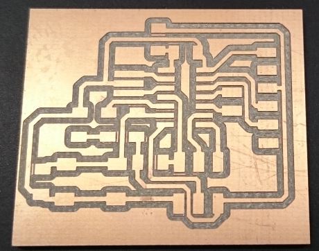
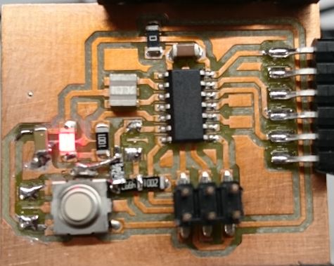
I reverse engineered the schematic from the board
pcb picture and redraw the schematic and layout with Eagle
using components from fab.lbr. The VCC and GND components are from
supply1 library. I added a capacitor in parallel with the push
button to filter bouncing glitches. The 100 ms time constant was a
bit of an overkill, and actually the operation of the falling edge
when the button was pushed was awful. The rising edge looked just
fine, but slow. Unfortunately, I forgot to document this phase. But,
I think that the unreliable switch combined with a large capacitor
produced extra pulses from the capacitor when the switch reopened
because of bouncing after closing by pushing. Without the capacitor,
the falling edge was OK with some overshoot, but the rising edge was
ruined.
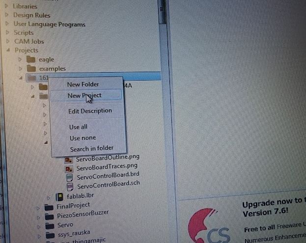
I setup a new project:
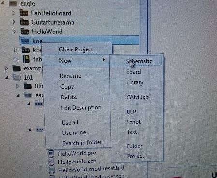
and created new schematic.
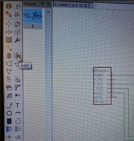
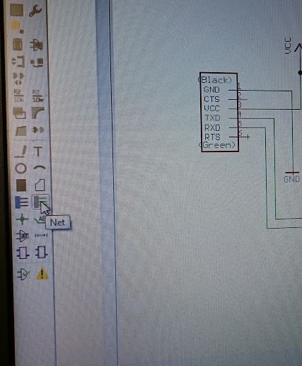
I added the components needed with the Add tool:
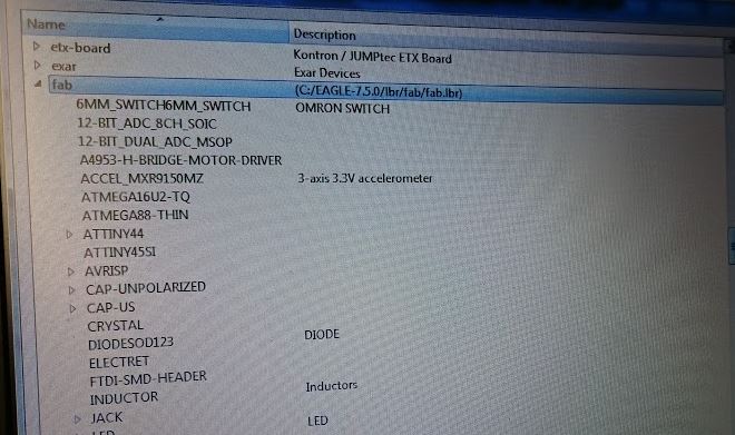
from fab library:
And wire the connections with the Net tool.
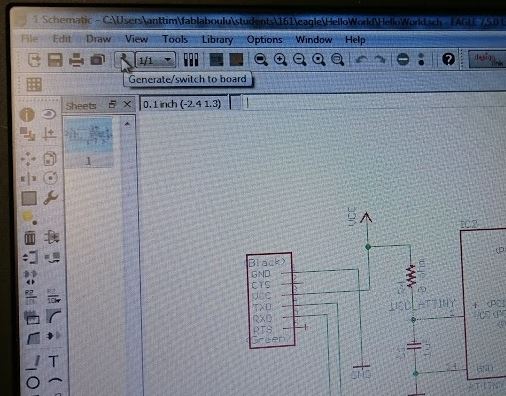
When the components were in correct places, I switched to board:
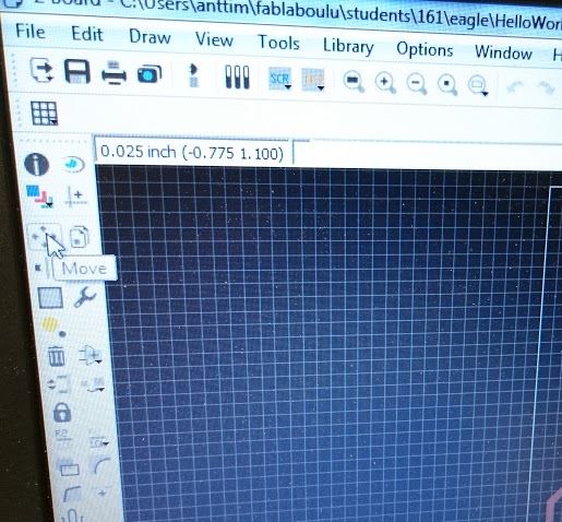
In the board editor I moved the components to their places trying to
minimize the wire lengths.
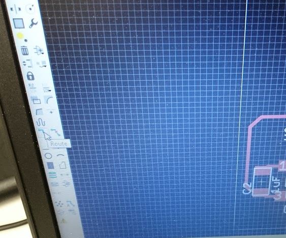
I setup wire widths:
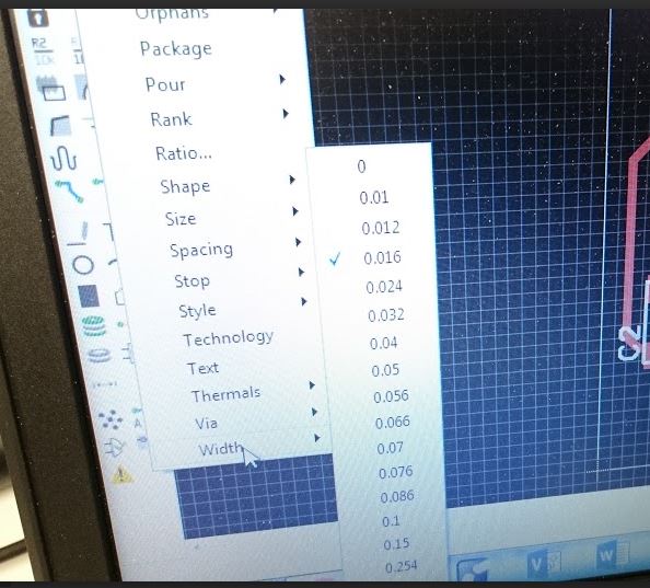
And created the copper wires with Route tool:
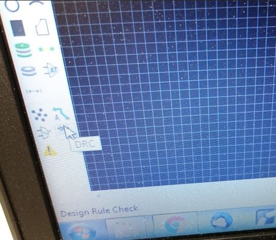
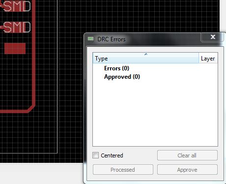
After routing I checked the design for errors:
And finally no errors were found:
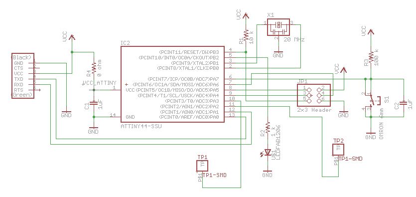
The schematic and layout look like this:
Fabrication:
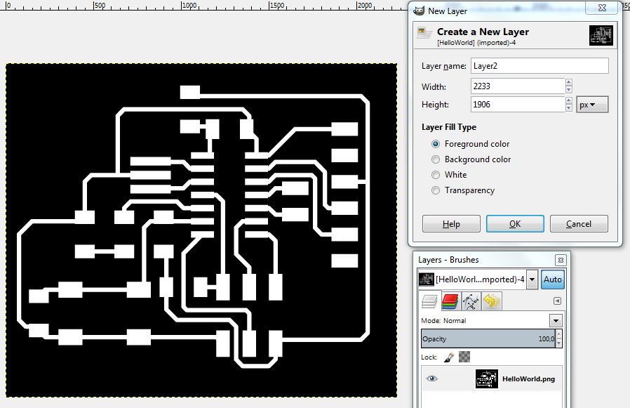
Then I exported the layout as png-image with only Top layer
selected. I opened the image in Gimp and went through the following
procedure:
1. Create a New Layer with foreground color (black). This is for the
outline.
2. Move the original layer on top to make it visible again.
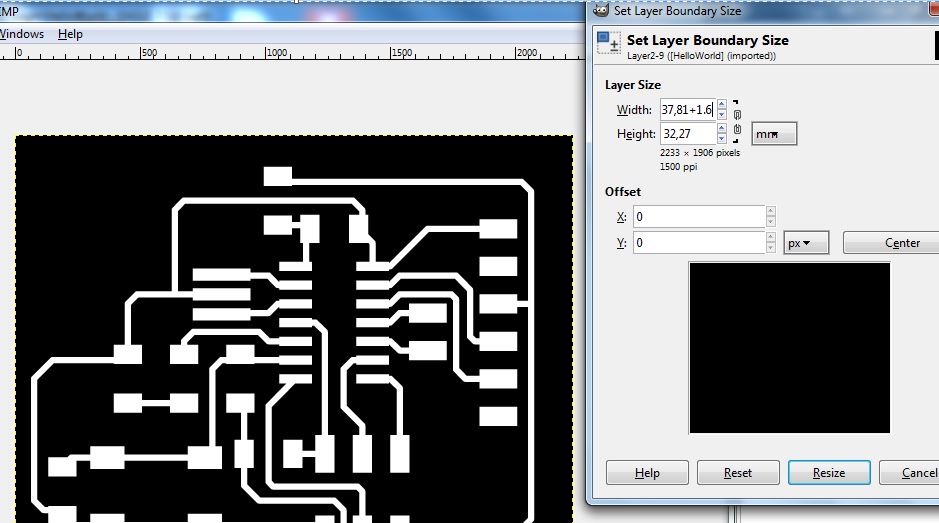
3. Set Layer Boundary Size for the newly created layer. Add 1,6 mm
to width and height centered. The 1/32 (0,8 mm) milling bit takes
away this much.
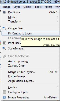
4. Fit canvas to layers. The canvas size is the size of the new
outline layer.
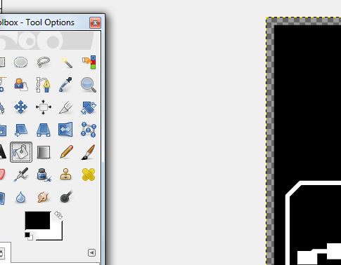
5. Color canvas black with bucket tool and black foreground color.
The checked outline in the picture below is the outline of the final
exported outline picture. Now we color is black.
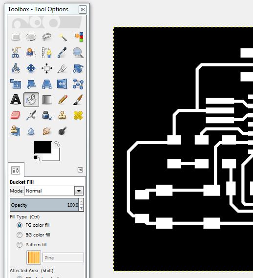
6.Export png-image for traces. To keep the same origin in both
pictures, the traces is exported with the outline.
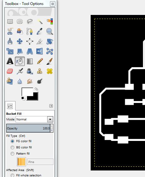
7. Swap the order of foreground and background. Then fill the
original layer with traces white with the bucket tool. This leaves
us with the outline.
8. Export png-image for outline.
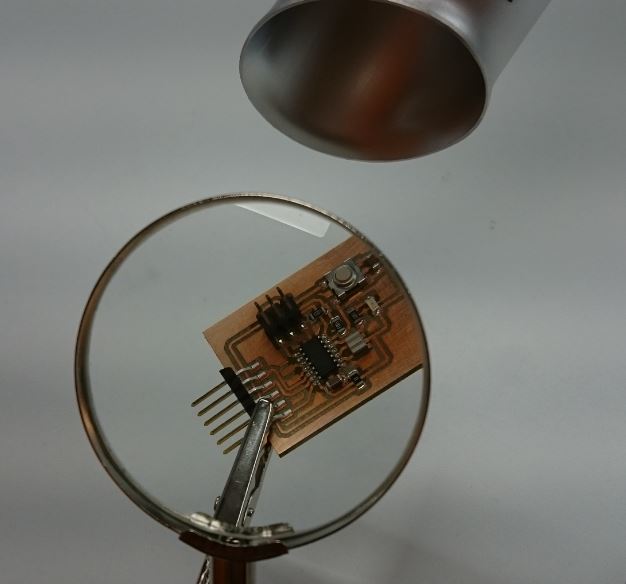
The board came out just fine.
50+ designer needs optical aids. Don't forget exhaust for soldering
gases! It also keeps the fire department away.
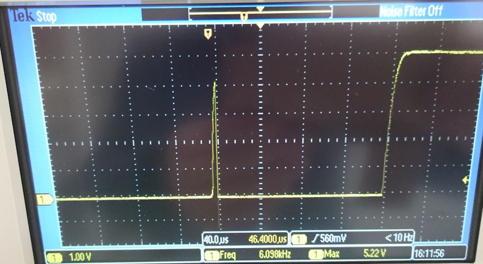
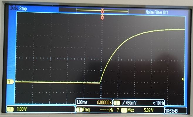
Testing the push button:
The picture below shows an example of a bad push button behavior
when the button is released. And every time it looks different.
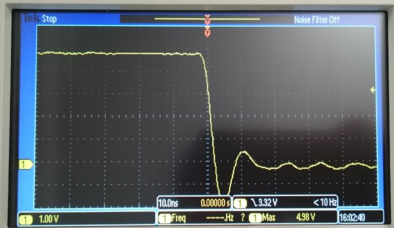
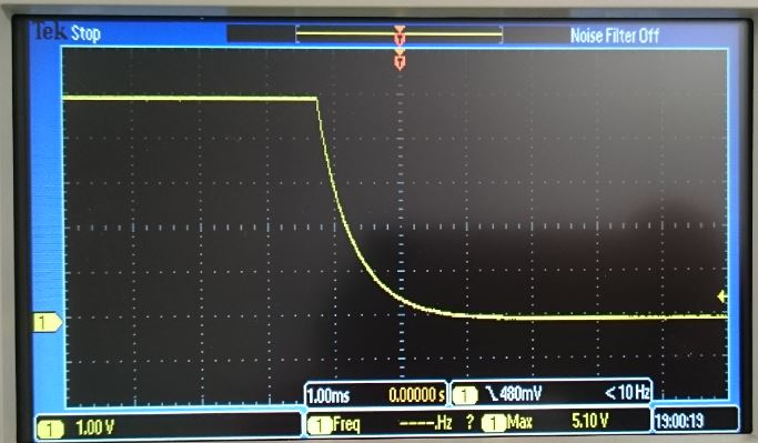
The picture below shows the behavior of the falling edge when the
button is pushed. The capacitor is removed.
Below is the modified schematic with improved push
button debouncing. R5 could be bypassed with a diode to have
more symmetrical time
constants for charging and discharging the capacitor. Now the
charging time constant is 1 ms and discharging time constant is 0.5
ms. As a result, the falling and rising edges of the push button
signal are clean without glitches. Combined with the Schmitt trigger
input and the synchronizer of ATtiny44A (page
54) this gives a reliable operation for the switch in the hardware
domain. If I ever use a push button again, I will consider using a MAX6816
switch debouncer and stop worrying.

Modified board:
Clean button release:
Clean button push:
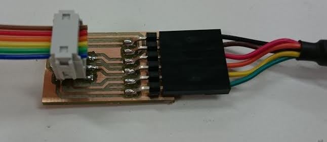
Jani asked me to contruct a cable for connecting the
FTDI-USB-TTL-232-cable to ISP-connector, so that we could try bit
bang programming. I decided to make an adapter. The order of pins
came from there:
http://doswa.com/2010/08/24/avrdude-5-10-with-ftdi-bitbang.html
http://doswa.com/2009/12/20/sparkfuns-ftdi-basic-breakout-as-an-avr-programmer.html
 FTDI   +-------ISP------+   FTDI
 [RX]--o| 1 MISO   +5V 2 |o--[5V]
[CTS]--o| 3 SCK   MOSI 4 |o--[TX]
[RTS]--o| 5 RESET  GND 6 |o--[GND]
        +----------------+
Files:
HelloWorld:
- schematic
- layout
- traces
- outline
ISP_FTDI:
- schematic
- layout
- traces
- outline
Home