The assignment for this week was to redraw the echo hello-world board adding a button and led while checking the design rules and making it. Optionally, we could simulate its operation for extra credit.
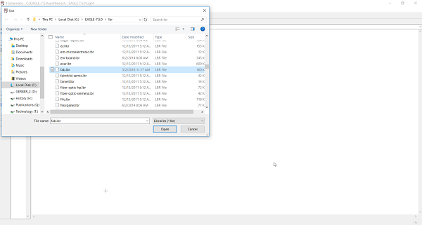
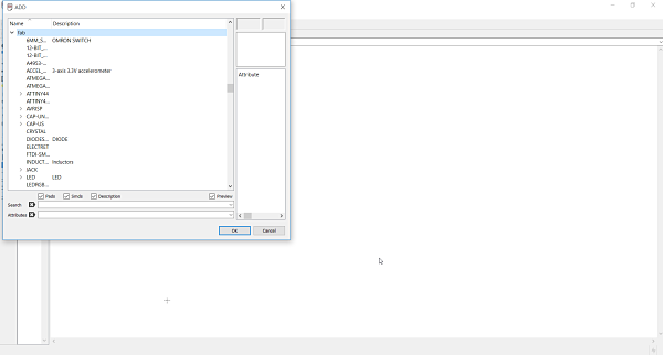
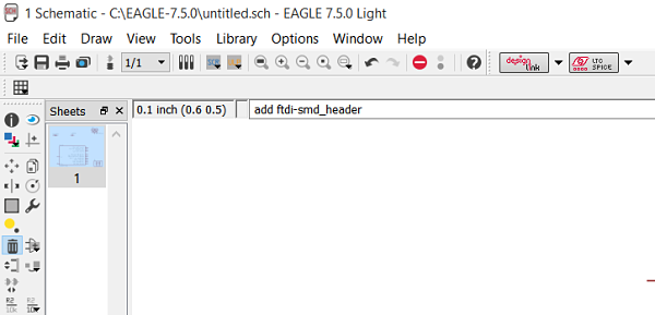
I decided to use Eagle software to design my board. I went to the Eagle site and downloaded the 64 bit Eagle software version 7.5.0. I then loaded the much discussed FabLab component library, fab.lbr. This allowed me to load the FabLab components into Eagle. I opened Eagle and checked to see if the fab.lbr was downloaded correctly. It was and I was able to add components to my schematics by either command line or using the GUI Add button.
Installing fab.lib in Eagle 7.5.0(L) | Checking To See Fab Components in Eagle 7.5.0 (R)
I then needed to learn how to use Eagle to create the design for my board. I decided to use the tutorials posted on the FabAcademy.org website. I followed the directions and read all 9 steps listed in the tutorials to provide me with the steps need to complete the process. I realized it would take some trial and error along the way. I also watched this YouTube video as an introduction on how to set up the schematics. It was a nice visual walk through of what I needed to get started building the schematics of the board.
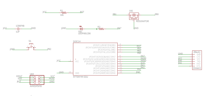
To create the schematics, I needed the list of components that I needed for the board. Once I secured the components needed I could easily choose the correct component from the fab.lib in Eagle to create the schematic. The components I needed were:
I then opened up Eagle and started to create the schematic for the board. I did this at first by using the command line to insert the components into the board. I quickly then started to use the GUI as it made it faster for a novice like me. I very quickly started to add all the components and then the labeling process began. This made it easy to connect all the GND's together and as I labeled the schematics it all started to tie together.
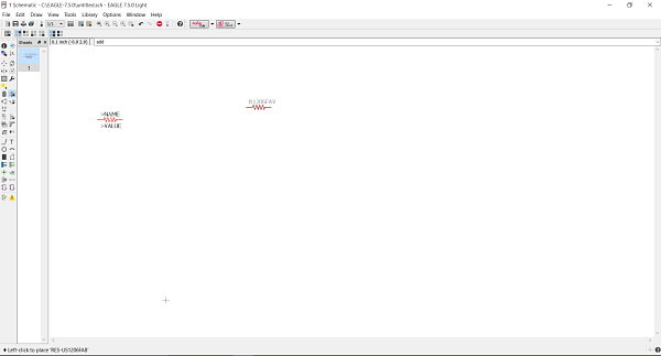
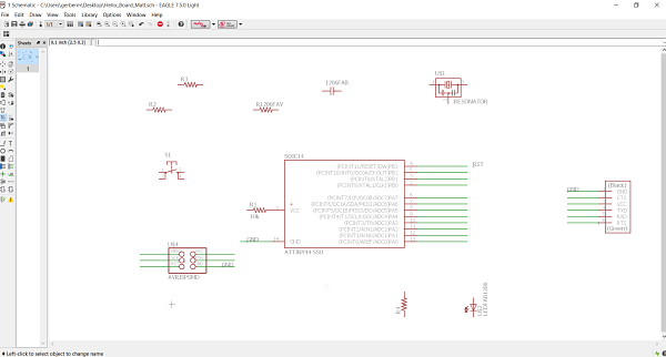
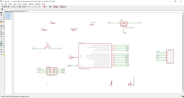
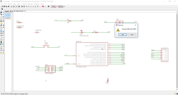
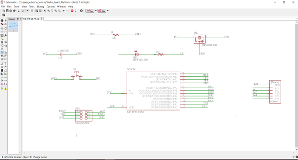
The Process of Building the schematic using command line and then GUI
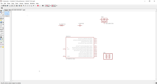
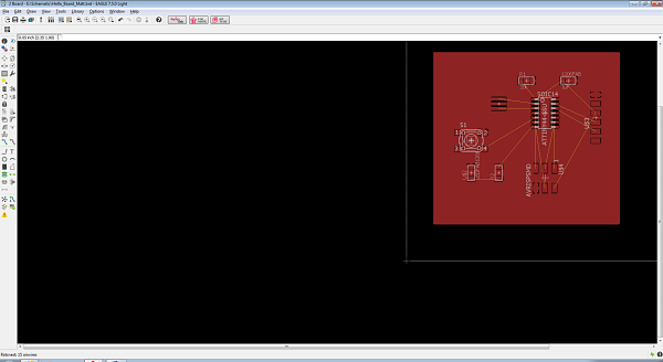
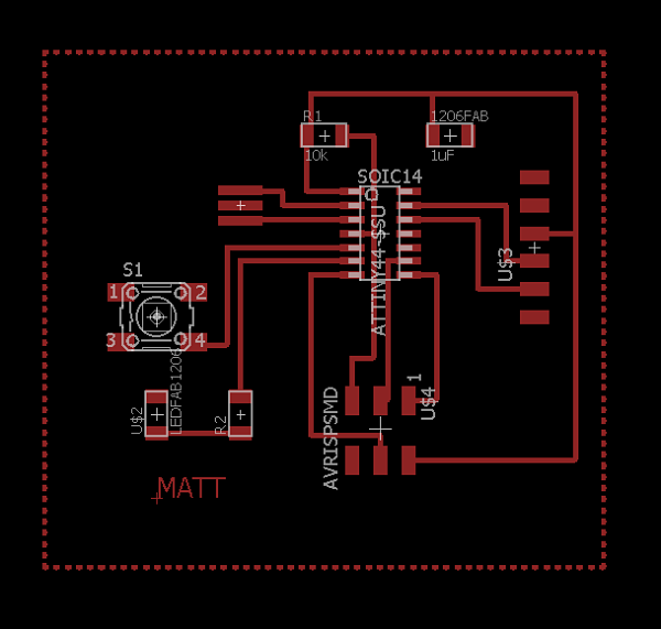
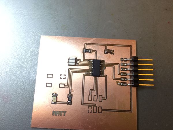
This is the finished schematic.
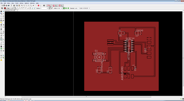
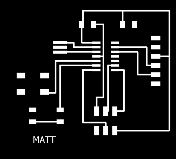
The next step was to be able to place the components on the board. In Eagle I switched over to the board view. I was then able to start placing my components to create a traces on the board. The components were placed in the corner with the yellow lines attached. I then looked at Neil's board to get a sense as to where to place the components for efficient traces or routes on the board. It provided me a sense of where to potentially place components. I then started to sort the components on the board. It was fairly easy to drag the components around.
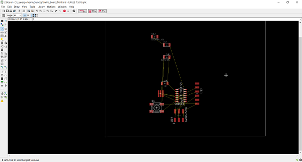
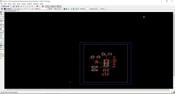
I played around with the autorouter feature. It did layout the board, but I found it did have a few issues on how it layed out the board.
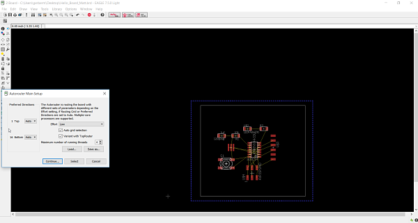
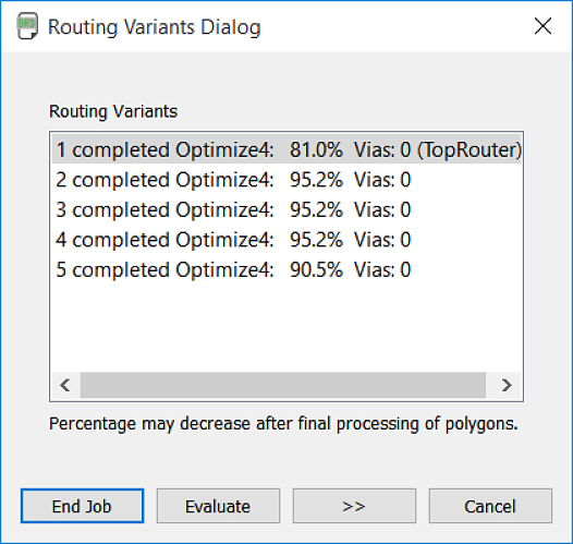
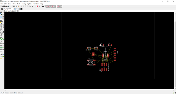
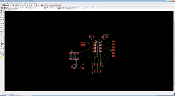
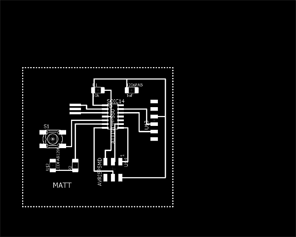
I discovered it was best to just hand route the board. I decided to start over and my final board came out close to the example provided by Neil. I started with the ATTiny44-SSU and built the board around it. I then started the process of hand routing the board based on the examples provided in class. I added a ground plane as recommended by a member of our class. We discussed it and it can reduce noise and I found it pretty easy to add. This takes all the unused space on the board and connects it to the ground net. This can make it harder to solder, but I find the soldering part to be pretty easy. To make a ground plane you use the Polygon tool in Eagle. Click on the Polygon tool and select the top layer as we are cutting one sided boards. I draw the Polygon around the outside of the board or perimeter. I then used the Name command and clicked on the dashed red line I just drew around the perimeter and changed the name to GND. This was the same I used for the traces connected to the ground pad. I then right clicked the dashed red line and selected Properties. I made the width of the wire .016. I then ran Ratsnest and the ground appeared.
I then cut out the board and assembled my components. I did it in a similar manner by taping all the parts on a piece of paper. I decided to make two boards. I know this is risky because if the board design is poor, I just wasted materials. I only cut one board on the TinyISP and needed another because of the soldering job, so I decided since I live far from the FabLab to cut two boards so I would not have to drive back to work on it if I did not correctly solder or stuff the board. This proved to be very beneficial in the long run.
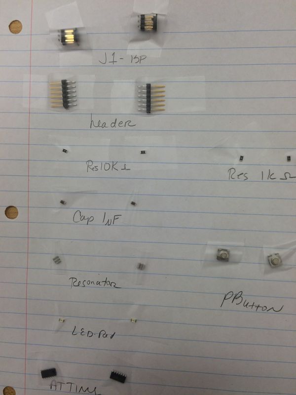
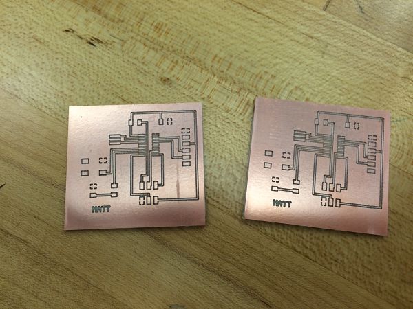
The Components Taped to Paper (L) | The Two Cut Out Boards(R)
The best part of the process the the ability to improve my soldering skills and use the microscope. I enjoy the process of surface mount soldering. I am improving with practice and I find it much slower, but enjoyable than thru hole soldering.
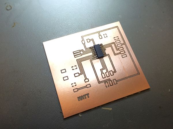
Adding Each Component on the Board
I am glad I cut two boards because I found that when I was soldering I let the solder dry and pulled the soldering iron away and tore the trace out. It was frustrating because I only had one component to solder. I then started on the second board. You can see the trace missing in the highlighted lower right. We tried to use a wire to connect the trace, but it did not work.
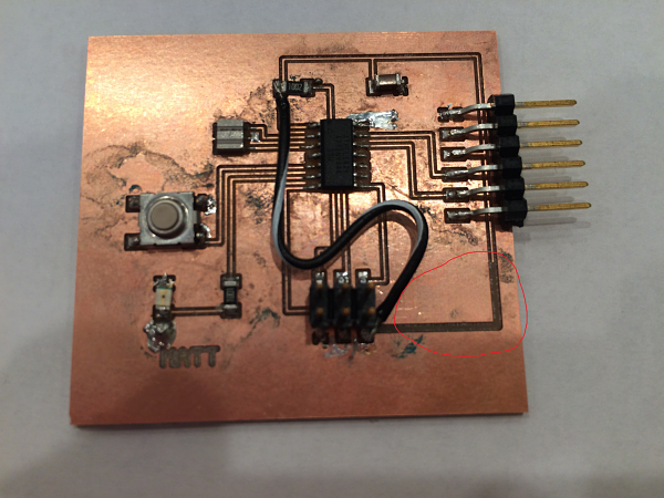
The Trace Came Out
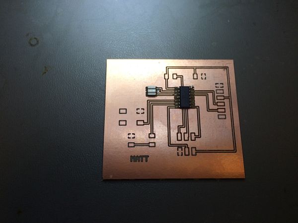
I then started on the other board and finished the soldering without any issues. It is illustrated below.
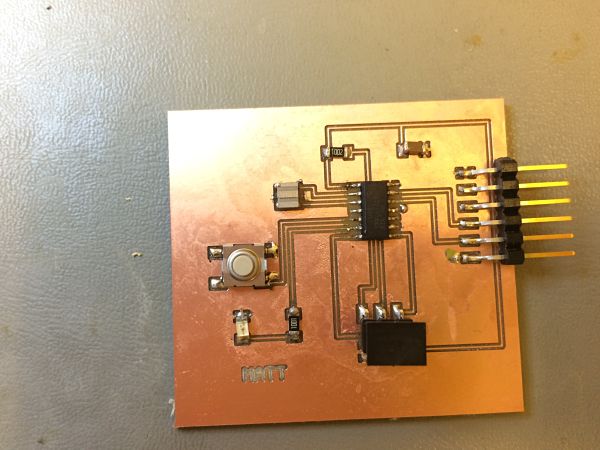
The Final Board
It was easier as I went along to affix the components to the board. Some of the components were harder to affix to the board, so I used the technique of putting some solder down before attaching the component. This happened for the switch which was probably the most challenging part to solder to the board because of its position. It helps to have professional solder irons. I am also glad I cut two boards initially to protect myself against the mistake I made.
Project Files: