In the sixth week we explore Electronics Design. This week we take electronics to higher level. We will edit an existing design adding a pushbutto, and LED and a resistor for the LED. Some sort of electronic CAD package will be used to create the circuit and then create the traces to be machined.
Here is a list of tasks as I see them for the sixth week.
I checked out a few of the pcb software packages available and selected Eagle-cad from CadSoft Computer. The name stands for Easily Applicable Graphical Layout Editor. I spent a few hours going through their tutorial. It was more

Here is a screen capture showing the turorial menu.
I decided to jump right in and start building a circuit. We are lucky at the LCCC FABlab to have an electronics area with people that can help us. With a few lessons on the software I was able to start drawing my own circuits.
After a short practice session I dove into the task of drawing the hello-world circuit. I think it took about 4 hours to re-create the original hello-world circuit.
Here is a picture of the original components of the hello-world pcb.
Here is a picture of the original board from the FABlab website..
Here is a picture of the original traces for hello-world .
I drew the schematic and the board designs almost simutaneously. I loaded the components from the FAB library into the schematic and used labels to connect the circuits. After each new label I changed over to the board design to see if the connections made sense. It took me a few hours of trial and error to get the hang of the software. Eventually I was able to create the original hello-world circuit.
Here is a picture of the components placed in an eagle schematic.
Here is a picture of the yellow lines showing my first connections using a labeling scheme.
Here is a sample board used for modeling.
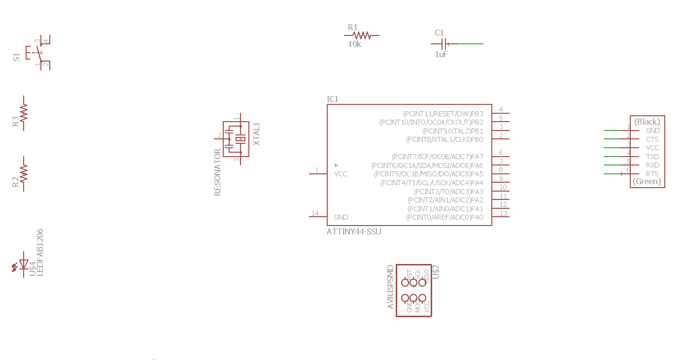
I aleady loaded the pushbutton and the LED with resistor into my drawing from the FAB library. All I had to do was label the connections and check the board drawing.
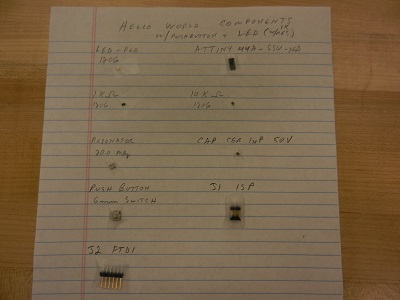
Here is a picture showing all the components needed for the edited hello-world pcb with pushbutton and LED.
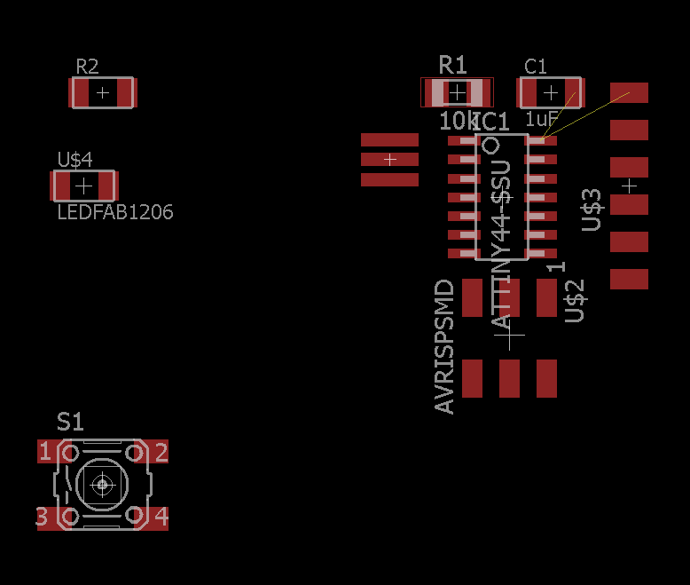
Here is a picture of all the components placed on a pcb in their final position.
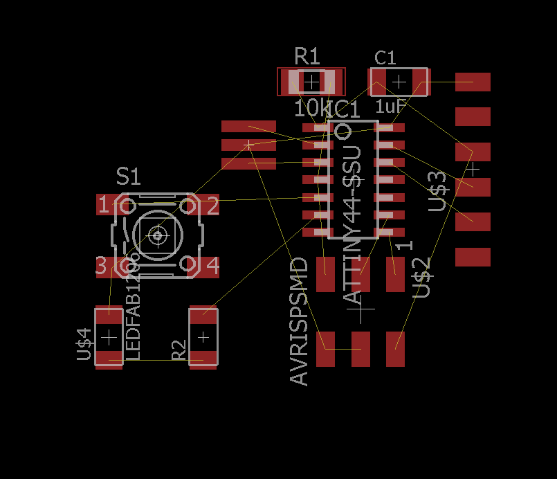
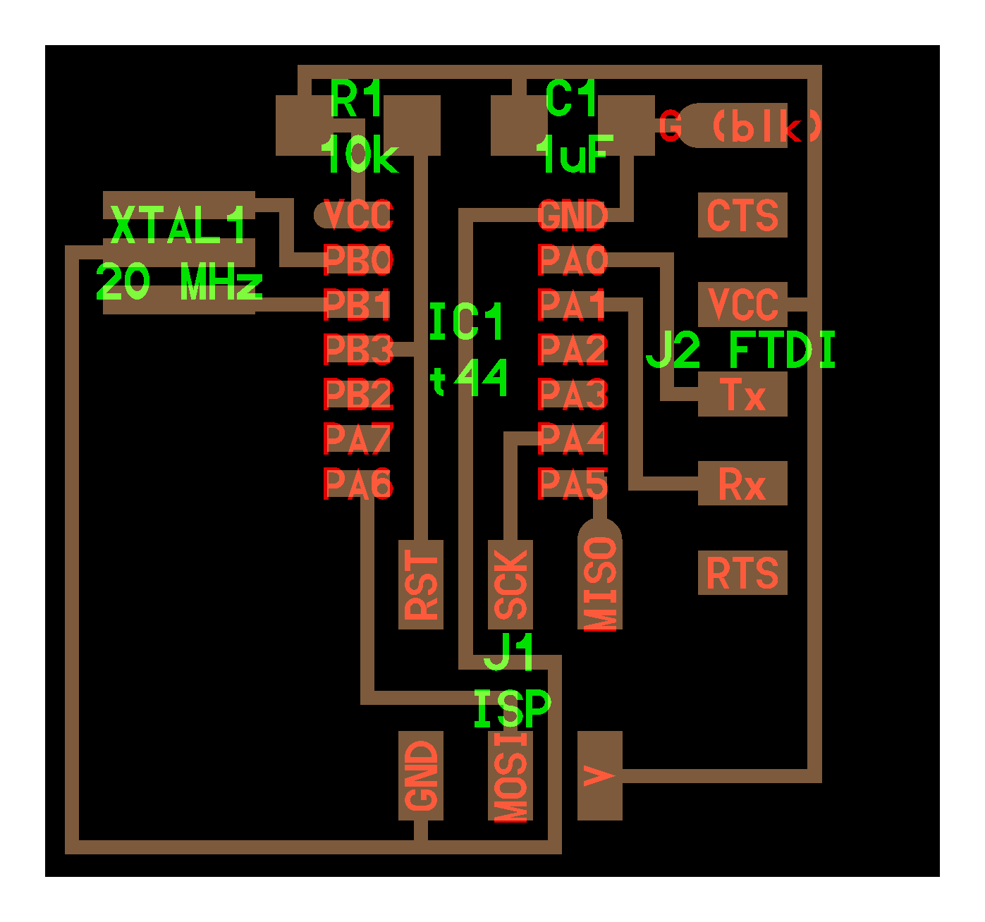
Once everything on the schematic and the board drawing checked out It was time to route the actual traces. in Eagle thin yellow lines are created when you are labeling the connections. You have to manually route the trace to complete the board. I was shown how to create a ground plane to cut down on the amount of machining needed to cut the board.
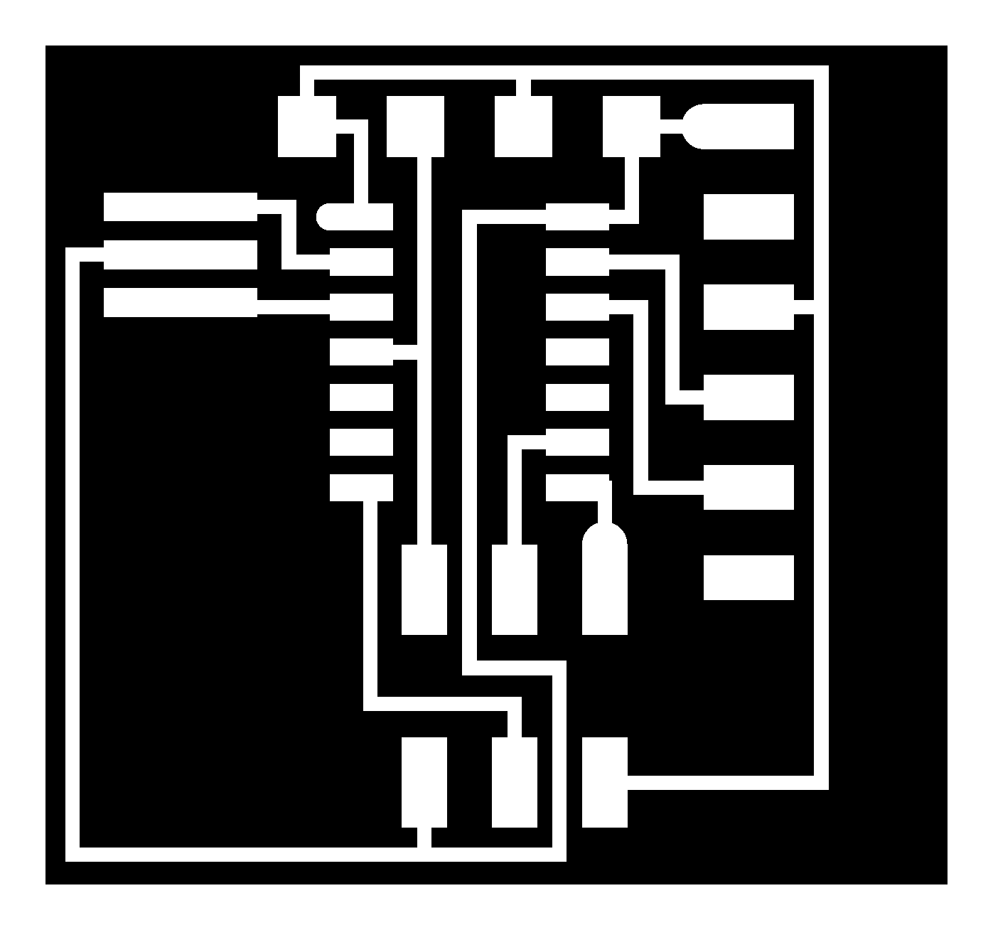
Here is a picture of the traces completed in eagle.
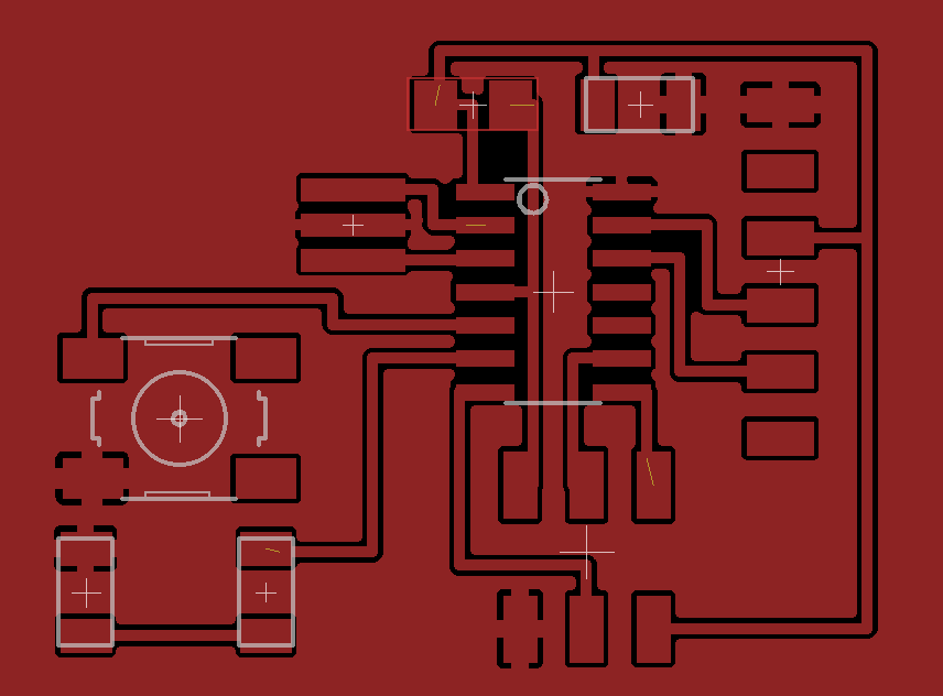
Once the traces were routed I used a CAM processor to create a Gerber file.
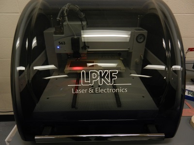
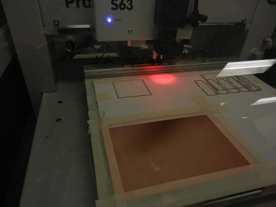
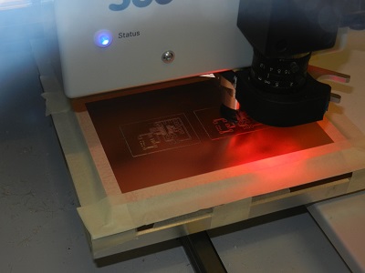
For my first PCB I used the Modela mill to cut the traces. I used an LPKF Protomat S63 electroics CNC to cut the new hello-world board with pushbutton and LED.
Here is a picture of the LPKF Protoamt S63.
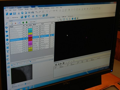
The Gerber file was loaded into the software and it calculated the tool paths needed to cut the board.
Here is a picture of the cam software I used.
The machine has an automatic tool changer and took about 30 minutes to cut two boards. I decided to make a spare just in case. The material is taped down to the table of the CNC and the board data is entered into the program. Once the program is executed the tool automatically changes and touches off to set the proper tool length.
Here is a picture showing the new material taped down on the CNC table.
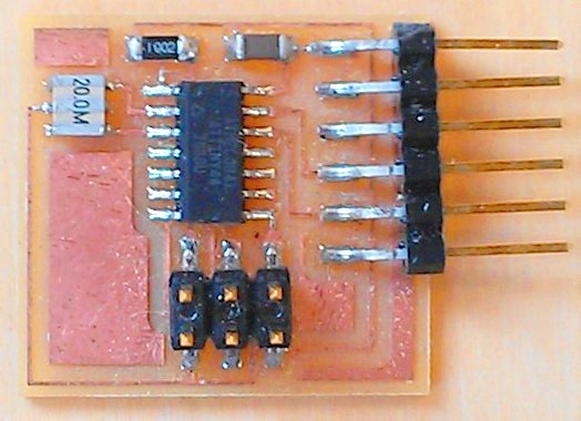
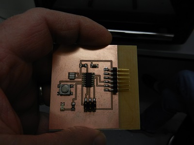
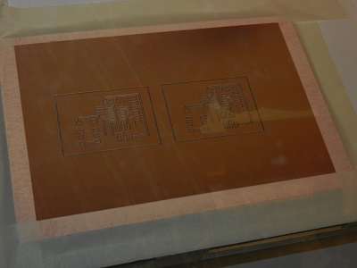
Here is a picture showing the finished machined traces..
Here is a picture showing the finished machined traces..
This being the second board I will solder I felt a little more comfortable.
Here is a picture showing the finished machined traces.
Here is a picture showing all the components needed to complete the board.
I set up all the components on a labeled piece of paper and started the process of soldering.
I did not have much trouble until I tried to solder the crytal.
I needed to presolder the trace to get the crystal to stick.
I used too much solder and had trouble getting the part to lay flat.
It looked like I had a trace pulling away from the substrate so I used some hot glue to help it stay in place.
It is a good thinkg I made a spare. I may yet need it.
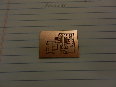
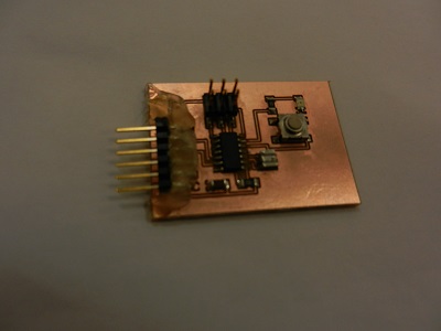
Here is a picture showing the finished soldered board.
The only problem I ran into was the traces pulling up from the board. I think I put too much solder down when trying to position the crystal.
I will try a little harder next time. I may try to get in some more practice soldering. I machined a spare board and have spare components if needed.