Week 11: Input Device
Simple Absorption Meter
Unfortunately, the RGB sensor is not yet available, yet. I am planning the design the ATTINY system
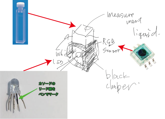
he concept is absorption measurement devise ("Called absorbance meter") for quick check of research. The input device is RGB sensor, and output device will be white LED. Currently I got S11059-02DT of Hamamatsu, and it requires I2C interface.


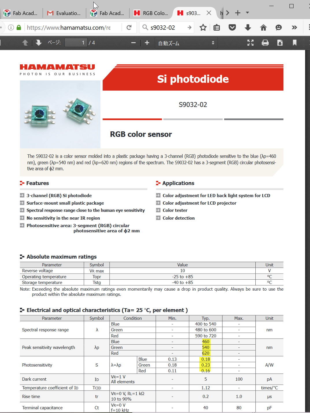
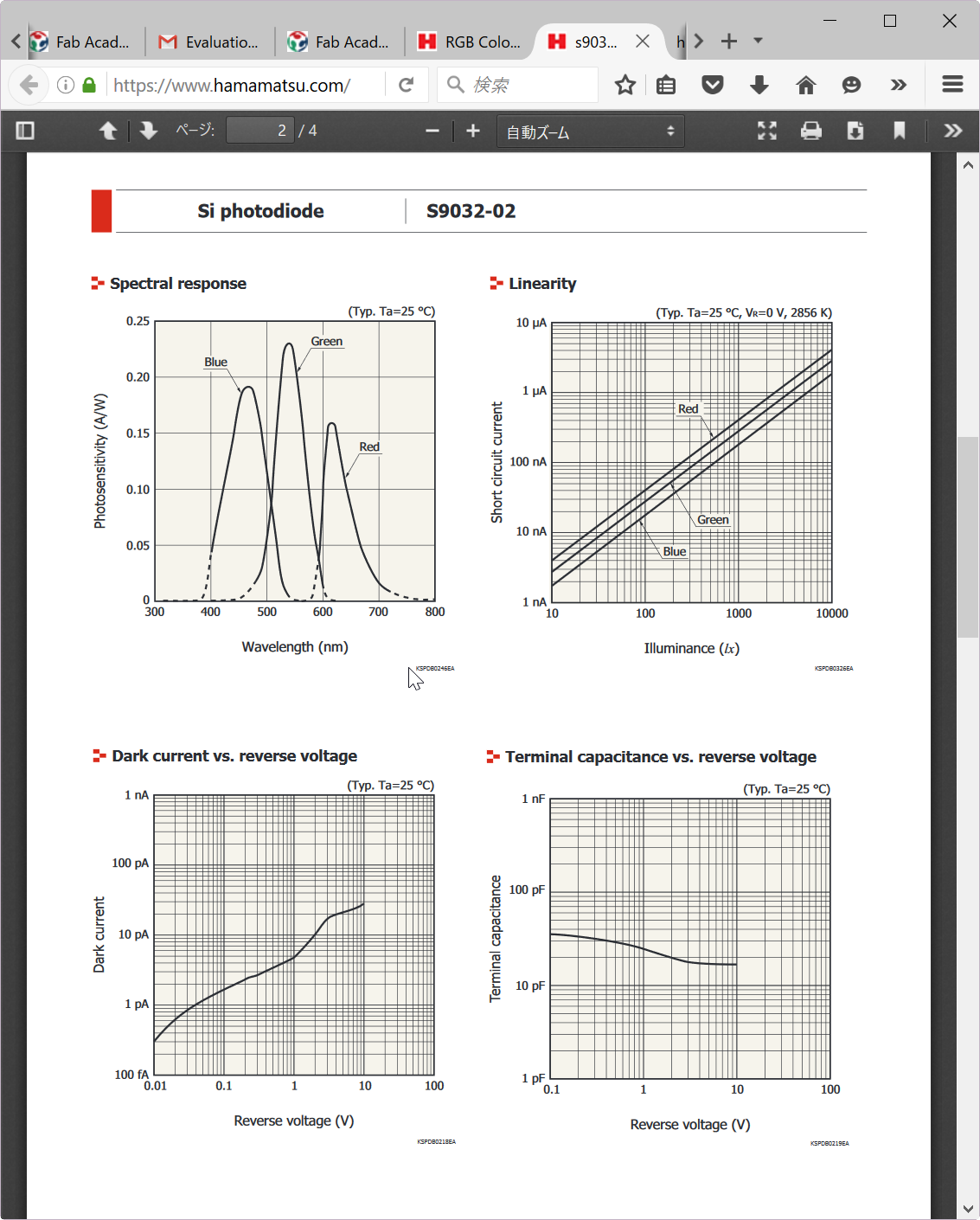
From the data-sheet, it is the cathode common type. The wavelength specification is as below.
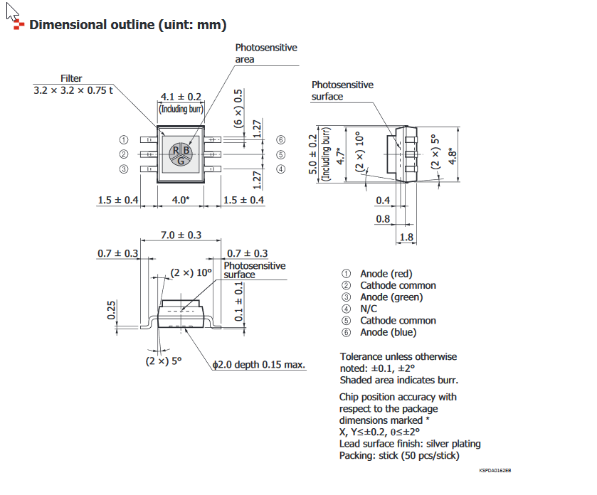
Since this device is not in the library of Eagle, I got dimension data from data sheet.
Designing ATTINY44 board for RGB sensor and 3 color LED
I add s9032-02 in new library (oki.lbr) from data sheet.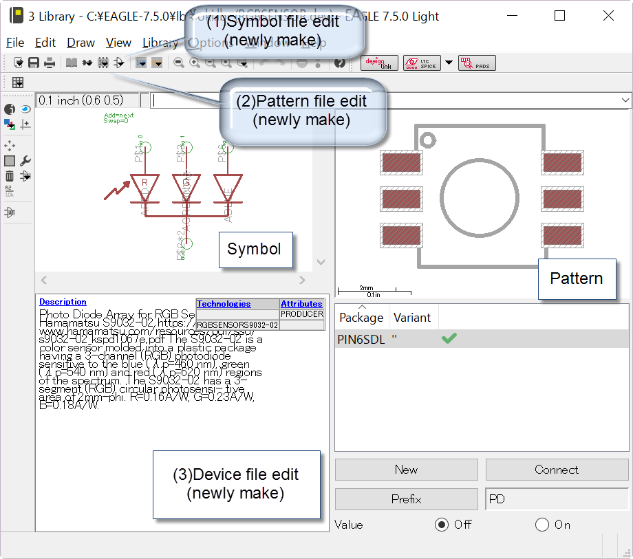
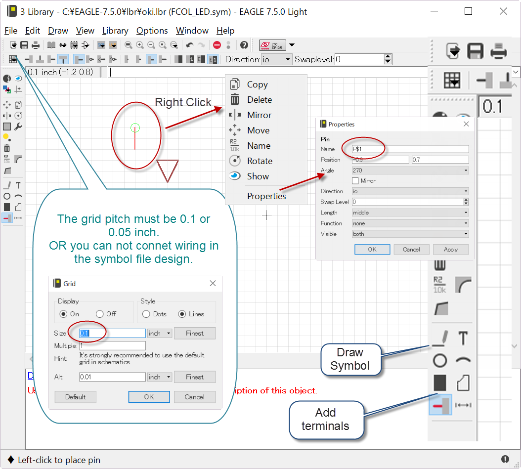
Firstly, I designed schematic file as following.
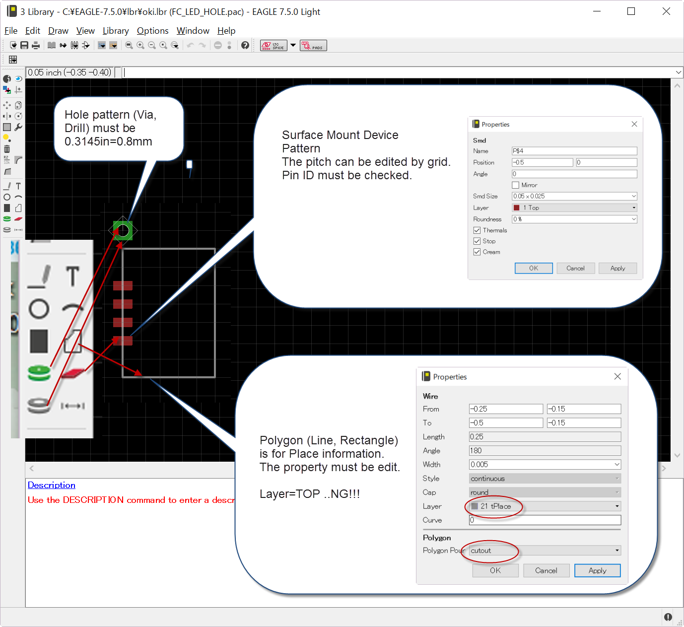
Secondary, I designed package file as following. The sign parameter were provided from data sheet.
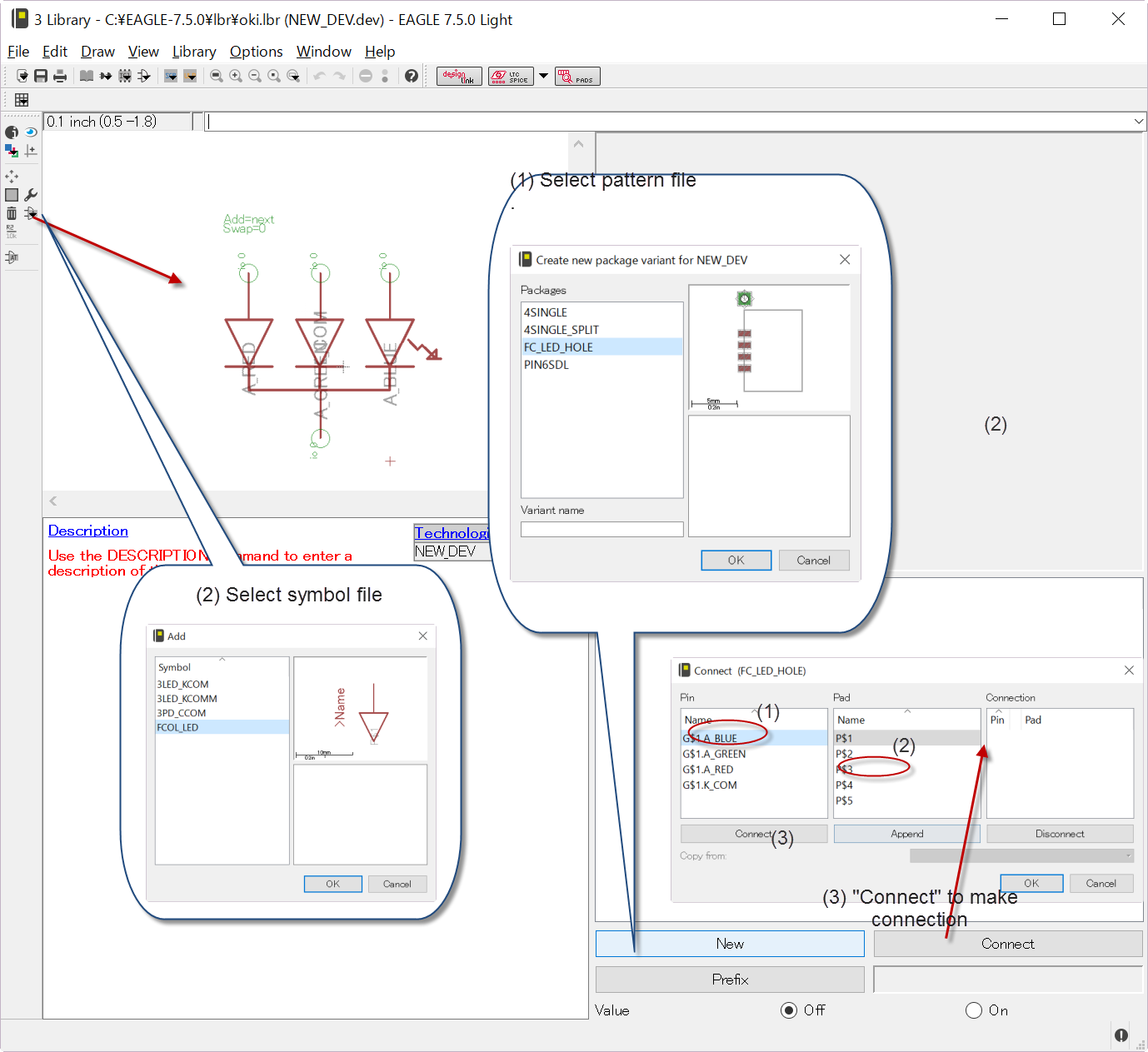
Finally, device file was prepared by specifying pins definition.
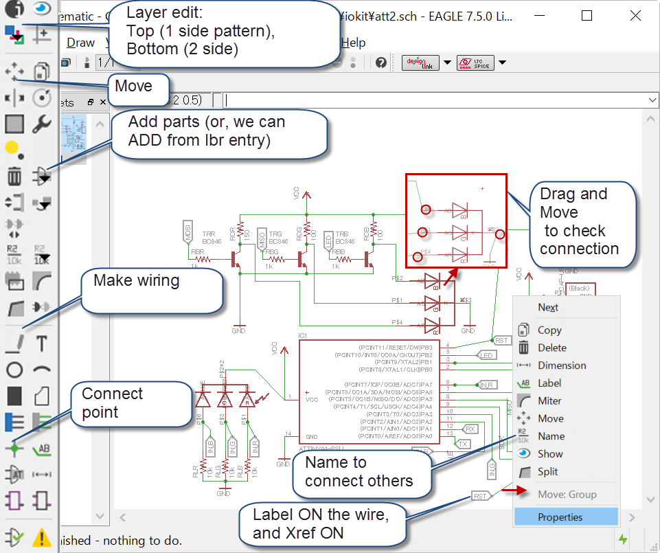
Here is the my library file for RGB sensor and full color LED.
And also, followings are the schematic file by the Eagle 7.5.
PCB fabrication
PCB milling for double side
A double sided PCB for input device was milled and fabricated. The board design file is as below.
Since I would like to put input device on the opposite side of the ATtiny and the other parts, I designed PCB in double sided, and local RGB sensor on back side.The milling software "Winstar PCB" was introduced for fine milling. (Unfortunately, this site is Japanese Only). This software can milling PCB based on BERBER data. The milling procedure is as follows:
- Design circuit in EAGLE and make brd file
- Make GERBER data in EAGLE. (foo.brd as example)
- In control Panel, Double click "CAM Jobs" > "gerb274x.cam".
- In "2 CAM Processor" windows, "File" > "Open Board" and select brd file.
- Push "Process Job", then GERBER data files are made in same directory. (extension is foo.cmp, foo.sol...)
- In control Panel, Double click "CAM Jobs" > "excellion.cam".
- In "2 CAM Processor" windows, "File" > "Open Board" and select brd file.
- Push "Process Job", then GERBER data for drilling file is made in same directory. (extension is foo.drd)
- Start "Winstar PCB". From menu of "Open GERBER", select foo.cmp for example.
- Many pattern in screen. Select "foo.cmp"(front) or "foo.sol"(back).
- Option "Customized Import" must be selected. 0.3mm for Pattern, 0.4mm for removing, 0.6mm for drilling and cutting. The data creation option "Highly analysis of Pattern" must be selected. And click "OK".
- The importing takes time. When the data appears on the screen, check the black-line (pattern cutting) correctly generated. If the electronic line is partially cut, you have to re-select 0.2mm for pattern and re-import GERBER.
- Add cutting frame. Then push "CAM-output"
- PCB milling is following process:
If double sided is needed, read foo.sol and pattern is fist. Then flip the PCB and mill with foo.cmp. Finally, finally cur the PCB.
- Select "cut" with XAL-BEM2S0.3 (Misumi) and depth is 0.04mm. You have to check the PCB board level. Tolerance is less than 0.1mm! If the PCB is slightly tilted, you can find carving width on Cu layer is not constant.
- Select "pattern" with XAL-EM2S0.3 (or 0.2) and feed of 0.08mm. The speed is 2mm/s for 0.3, 1mm/s for 0.2 are recommended. 150% faster may be possible for Paper-phenol. But for glass-epoxy 0.2 and faster carving would not work. This part is most important. For 0.6-0.8mm separated land can be obtained with 0.3. If you need finer result, you can challenge with 0.2.
- Select "remove" with XAL-EM2S0.4 and feed of 0.08. This process just remove remained Cu layer. This is optional.
- Select "hole" with XAL-EBEM2S0.3. Depth is 1.6mm. Down speed 0.5m/s.
Double sided of Glass-Epoxy PCB for "Input Device"
Blew is fabricated board Image. Front side is for ATtiny44 and everything except detector. 6 pins pin-header is for FTDI. 2 x 3 pins for fabISP. The back side on has the photo-detector. Blue-green glass is IR-cut filter. The board size is 30mm x 30mm.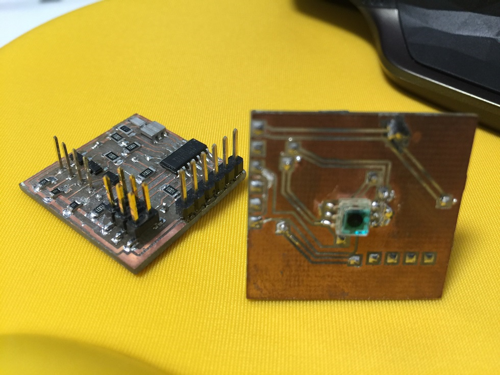
Programming Light Sensing from RGB Sensor
I tried the measure light with RGB sensor by changing the load resistance. The inputdevice.c program was made from Neil's hello.light.45.c. The code can be downloaded from below button. By using serial monitor, I got data from RGB sensor in text. I also tried to optimize the load resistance of the RGB photo-diodes. The results is as follows:- 10 kOhm
The signal level is around 14-35 in 10 bit ADC!. It was too small. - 100kOhm
The signal level is around 150-250. Still low but, summation can recover this problem. - 220kOhm-510kOhm To take balance, Above load must be better.