Week 6 - Electronic design
Re Design a Circuit
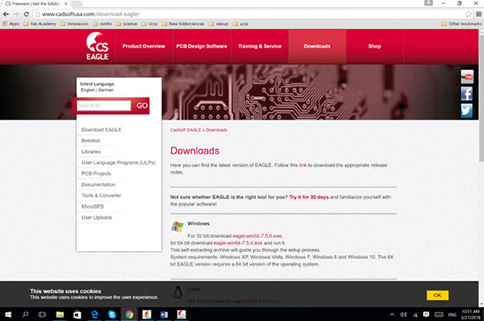
To redesign a circuit, I used Easily Applicable Graphical Layout Editor (Eagle) to re-design the “echo hello-world board”, I downloaded the Easily Applicable Graphical Layout Editor (Eagle) Version 7.5.0 for Windows (32 bit).
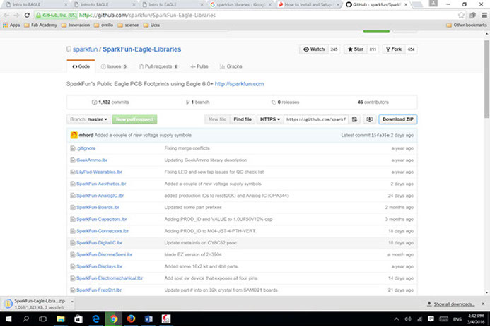
I downloaded the Fab Eagle library from http://archive.fabacademy.org/archives/2016/doc/electronics/fab.lbr
And the Sparkfun library from https://github.com/sparkfun/SparkFun-Eagle-Libraries
To use libraries, In the top toolbar menu select the "Library" option and then "use" option.
The following lines explain how to create a Project, Schematic and adding parts:
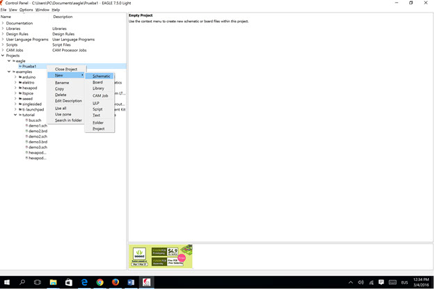
To make a new project folder . In the control panel, under the “Projects” option, choose the directory where you want the project to live and select “New Project”. To begin the design process, I add a schematic to a project folder, right-click the folder, chose over “New” and selected “Schematic”.
To draw the circuit, consider the following menu options:
- Inside the program: Menu/File/New/Schematic
- Menu/Edit/add: libraries components
- Menu/Draw/Net: connections between components
- Menu/Edit/Name: name to direct each output/input transistors
- Menu/Edit/Value: add value to components
First I added all of the parts the schematic sheet, then wire all those parts
When adding Components, It was very helpful to use the search tool, and looking for components that have as part of the description:
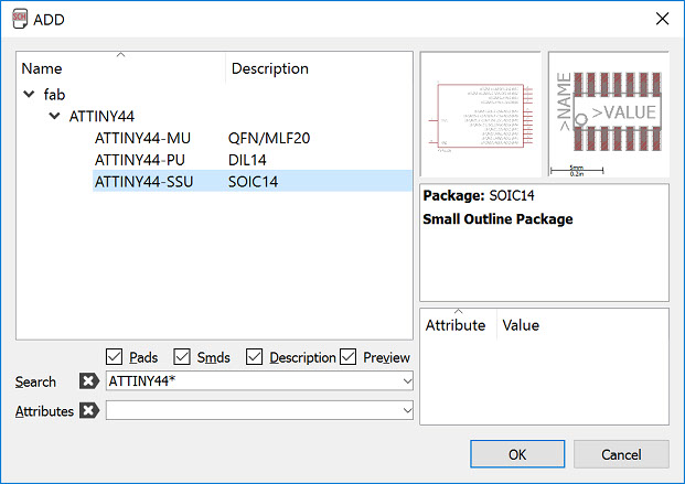
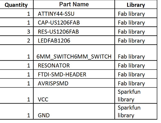
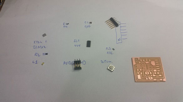
The components added were the following:
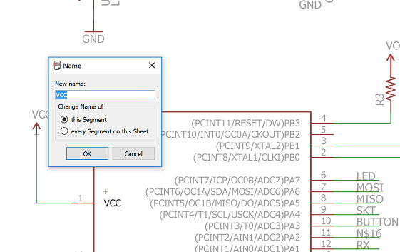
Connect the components with a "net", as is know a wire in Eagle. To avoid have a mess I used the “name” option to identify the connections and to avoid wires crossing each others.
In schematic view , Using the ERC Electronic rules check, to ensures the board will actually work
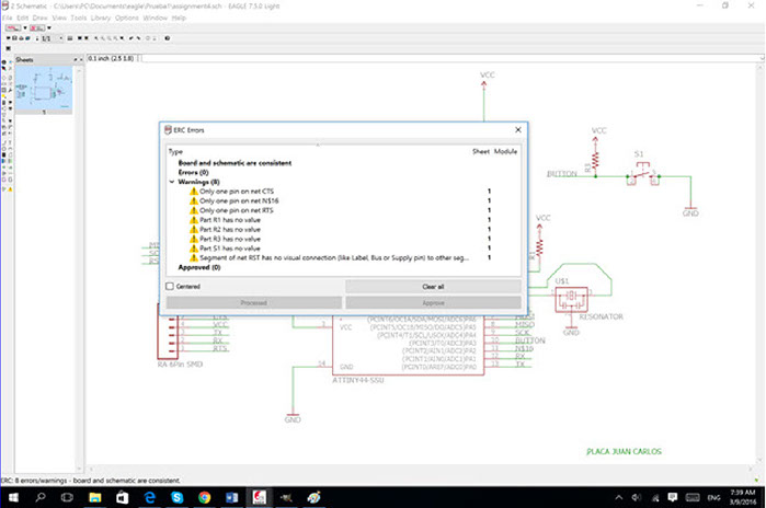
Only warnings messages are shown, they were aproved.
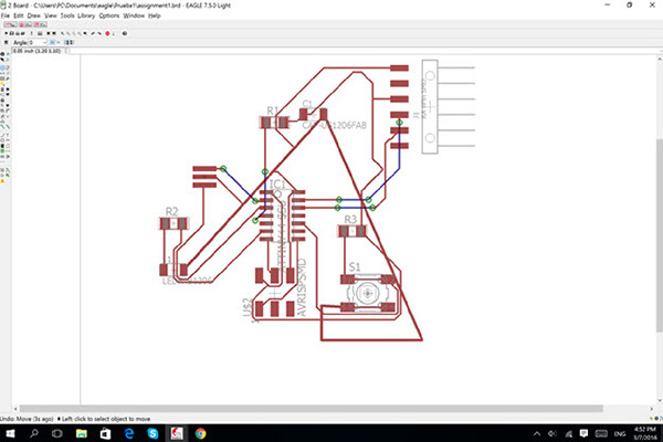
Next step is ReRoute the Traces on the Board
Consider the following menu options for this part:
- Menu/File/switch board
- "Move": To move the components
- Menu/Tools/autorouter: route automatically all the traces and then redraw the traces manually if the traces cross each other
- "Ripup": delete a trace.
- "Route": Draw traces for avoid the junction
Press the "Generate/switch to board" option. A PCB file is generated with the footprints of the components. The components just added appeared in a corner with unrouted traces attached. I Use "move" to move each individual component, and use route to build the route for each trace. For routing,first I used the “autorouter feature” but I prefer to move all component manual, to achieve the diagram: I used: Grid: 0.01 mm (View/Grid) Respect to the Design rules check (Tools/DRC/). I kept all the default settings, 16 mil for clearance. After some attemps, like the following one
Export to create traces and mill files
Menu/Layers settings: select only the traces layer (top)
Menu/export/image: Browse the file directory, check in monochrome and resolution 500 dpi
Open the image in GIMP
Reset canvas sizes to choose correctly work space
I achieve the following design
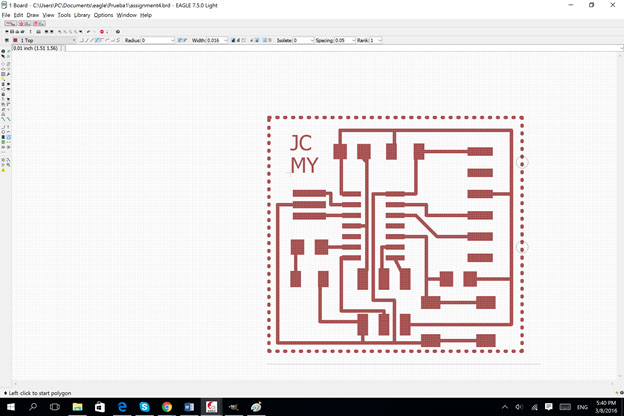
After that create the interior.
Making the circuit
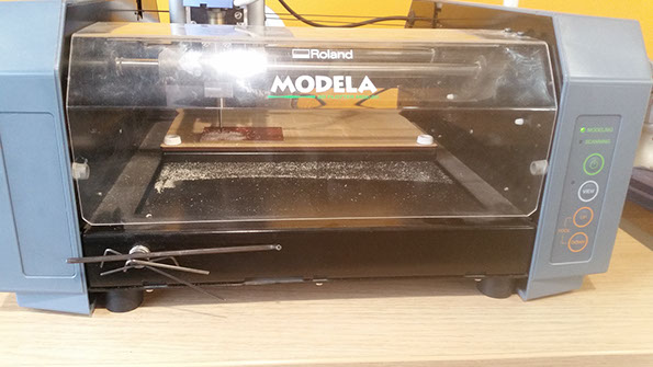
I exported the traces to .png (600 DPI, monochrome). I pick up my components and organised them. Using the Roland MDX-20 mill machine, I made the physical board. First milling, and after that cutting the PCB boards. I prepare to solder the components.
I exported the traces to .png (600 DPI, monochrome). I pick up my components and organised them. Using the Roland MDX-20 mill machine, I made the physical board. First milling, and after that cutting the PCB boards.
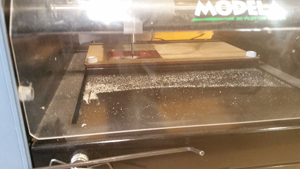
I prepare to solder the components
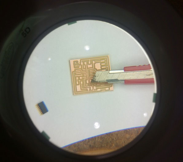
After milling, I had to cut some work that the mill machine didn’t do. Just one
For Soldering I used:
- Copper plates
- Tweezers
- Soldering iron
- Solder paste
- Solder
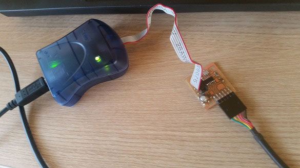
After soldering the components.
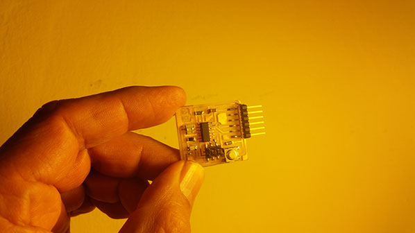
That is my circuit,
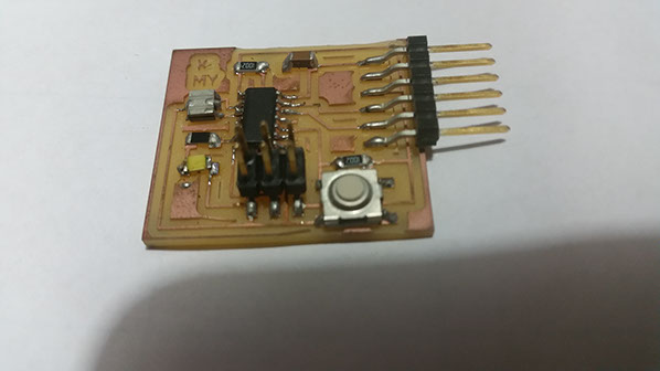
I test my circuit. It was ok.