During the team work and the machine design session, it became obvious that machines are more than stepper motors. The laser cutter we designed would need some control of the laser (turn it on/off, depending on the closure of a safety cover). It is a matter of safety !
Other machines projects also show the need for various sensors (temperature for hot wire cutters, and 3D printers) or various effectors (like servo-motors or relays).
It is possible to use input/output board as used in week 11/13. However, it would be great to have boards that could fit in the Gestalt framework, using the same network. Gianfranco Caputo (FabAcademy 2016 at Fablab Torino, Italy) made a great stuff: an Arduino shield to include the Arduino as Gestalt node substitute, allowing to drive a servo motor. In Ilan Moyer GitHub repository, there is also the extruder version of the Gestalt node.
My final projet is to rework the gestalt node to remove the H-bridge and components needed for the stepper drive, and replace this by a connector, that would allow to plug input/output boards connection. It also needs to be reworked to be fabable, which is not currently the case with the sophiticated double-sided PCB.
It fits well with the idea of Fablab 2.0, and MTM. It is centered on the embedded electronics design and networking.
To release the constraints, I also decided to use the bottom side as ground plane and place vias.
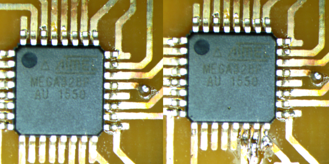
Using the previous stable version of KiCAD, I had to redraw or modify several non-standard modules (connectors, quartz, push_button). They are included in the archive below. I picked-up Atmega module here.
I made a first fabrication attempt, and made some minor changes to ease assembly (larger pads size for connectors essentially, and thicker traces). The final design is below.
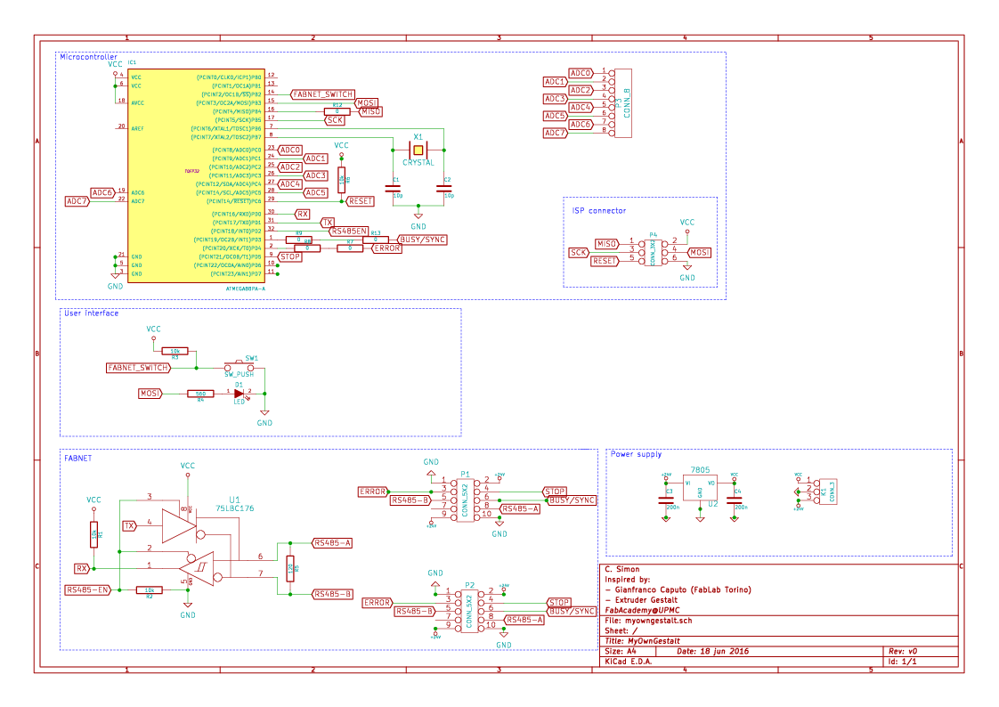
Here is a snapshot of the work under KiCAD: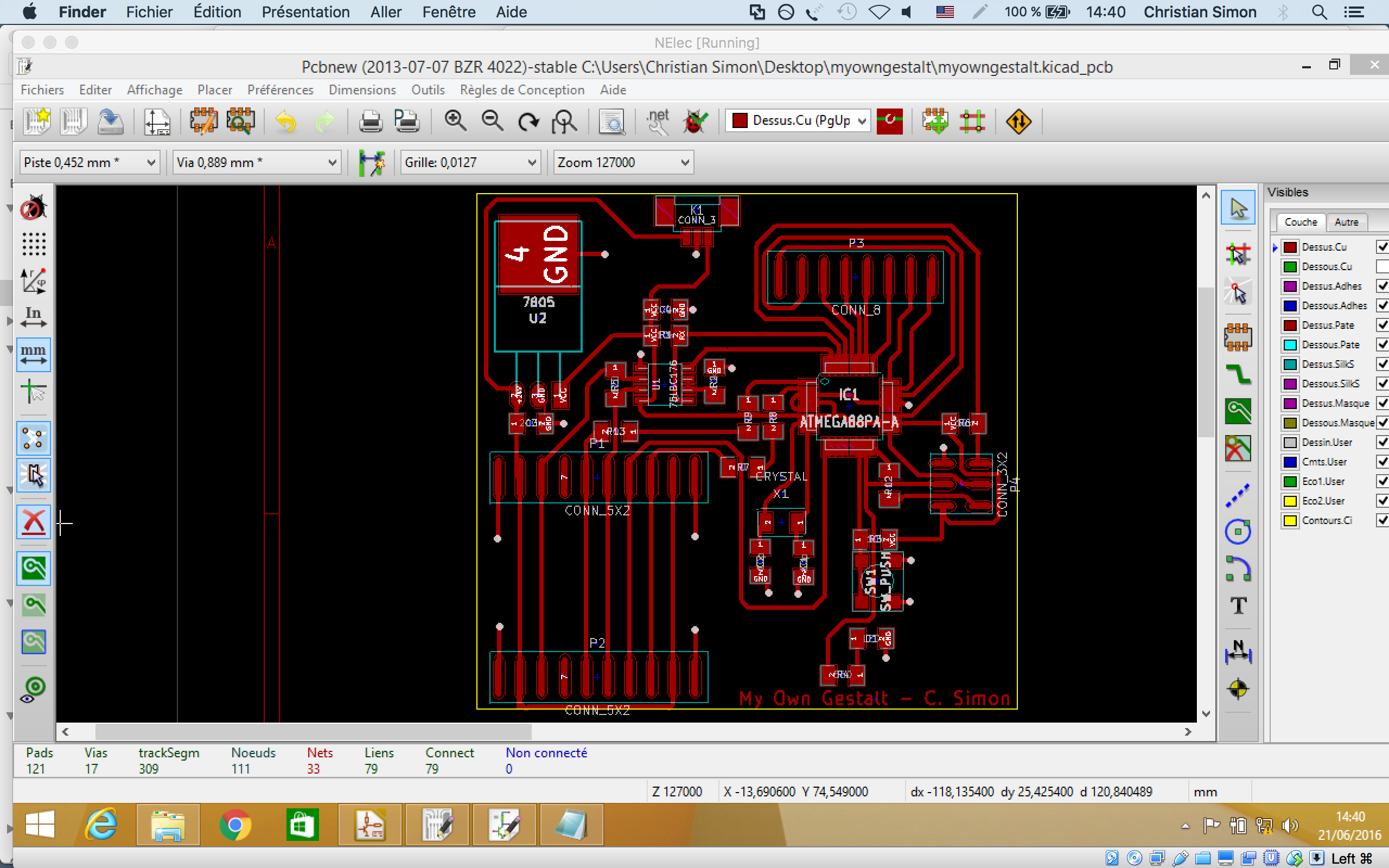 The final schematics is here:
 The final PCB:
 KiCAD project archive
I milled the first PCB with the Roland MDX-40, using the same parameters as described previously here.
I had encountered strange problem with FabModules (using Chrome) for the edges of the PCB. The Top layer exported from KiCAD as SVG from KiCAD is always fine, but the Edges layer seems to generate corrupted files. The RML file contains lot of NaN coordinates, but the preamble and the termination of the file are OK.I had to rework manually the RML file, from the Top Layer RML file.
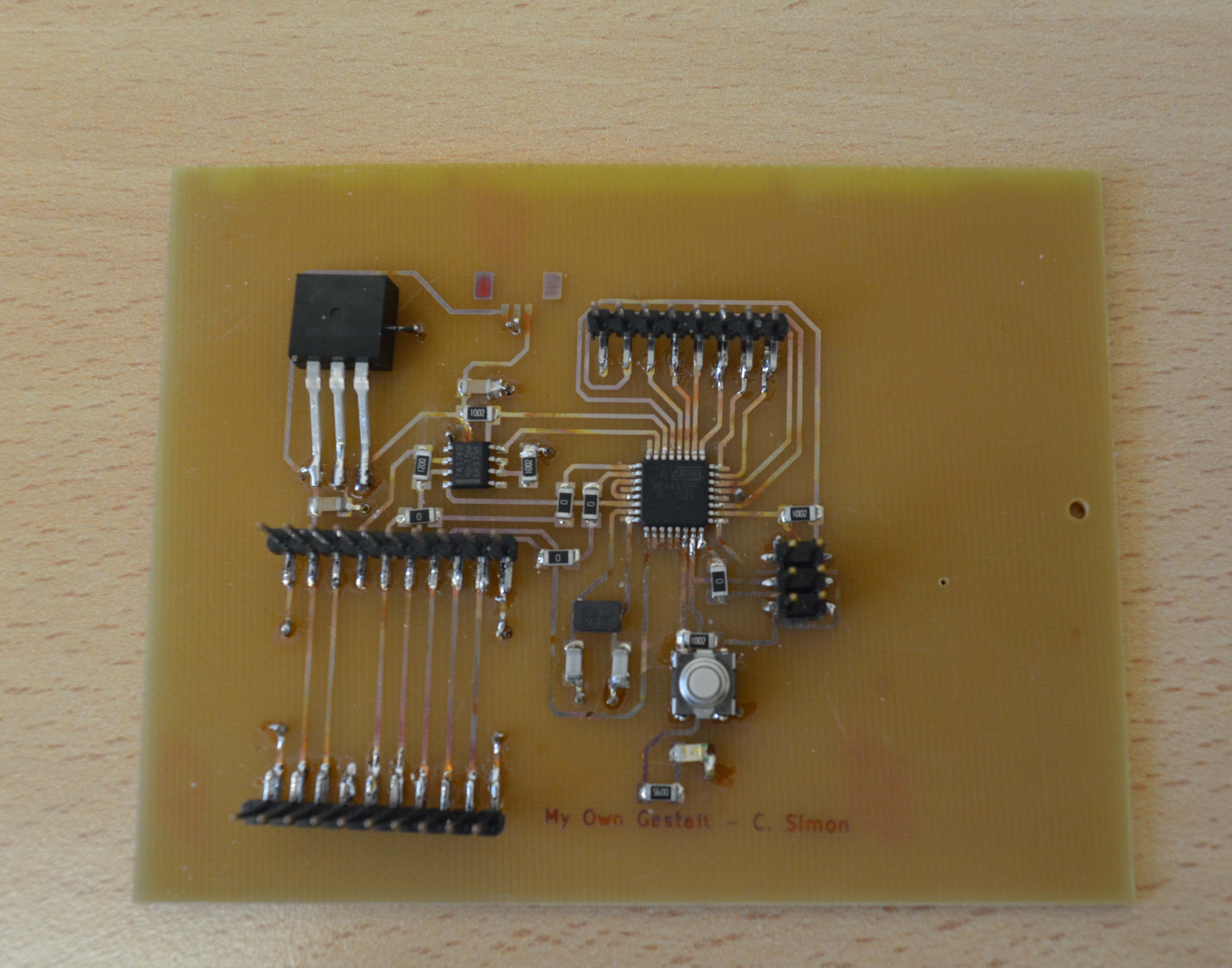
This first board took one day for soldering, under the binocular. The attemps to use solder paste with laser cutted stencils were disappointing (far too much solder paste, at least around the Atmega).
The copper layer has produced lot of little noises during soldering, even when proceeding rapidly and gently. I reallized later it was a sign for the traces lifting from the PCB. The double sided layer PCB was also behaving strangely: the solder was dewetting the copper. I never had seen this before !
The first board finally mounted
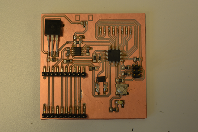 Many traces are far too thin.
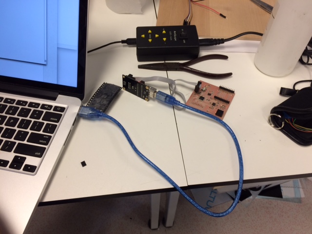
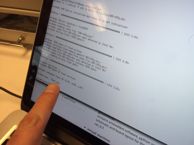
After assembly, the board was programmed (see below). During SPI connector removal, three of the six traces of the connector were peeled-off.
Many traces are far too thin.
After assembly, the board was programmed (see below). During SPI connector removal, three of the six traces of the connector were peeled-off.
Solder paste was applied manually under the binocular. All the components but the connectors and the push-button are placed manually. The the board is heated in a cheap reflow oven for 7 minutes at 170 C (3 min plateau), and at 220 C (one minute peak). The connectors and push button are manually soldered.
The overall fabrication time is 3 hours only.
Flashing the board failed: all the contacts involved are then checked again: it appears the MOSI pin is no connected properly. I had to resolder it.
After the presentation, Niel asked me to make the whole thing more robust, so it can be put on a machine without difficulties, and to focus especially on the connections.
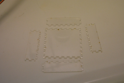
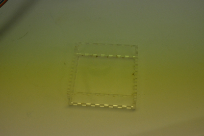
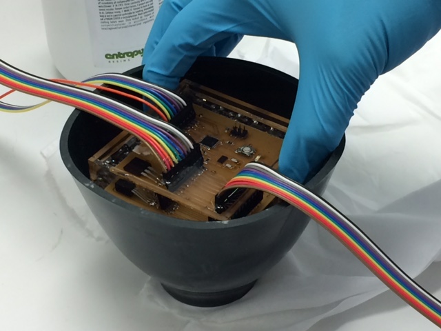
Throughole connectors are not a viable solution: this would require to isolate the connectors from the bottom ground plane, and loose the benefit of the current design. I therefore decided to try an encapsulation of the node: make a box of plexiglass, pour epoxy resin above it, cure !
 |
 |
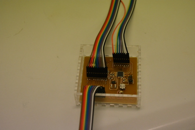 |
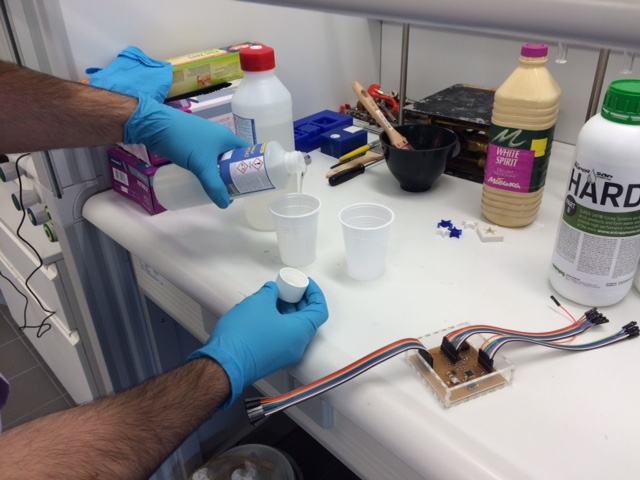
The non-toxic epoxy resin is mixed just before being poured in the box. The filling was operated in a bowl to prevent leaking/overflowing. However, the press-fit assembly is tight enough, and the mixture epoxy+hardener is viscous enough to prevent leaking.
 |
 |