PROJECT_06_electronics_design
Re-Draw the Hello Board
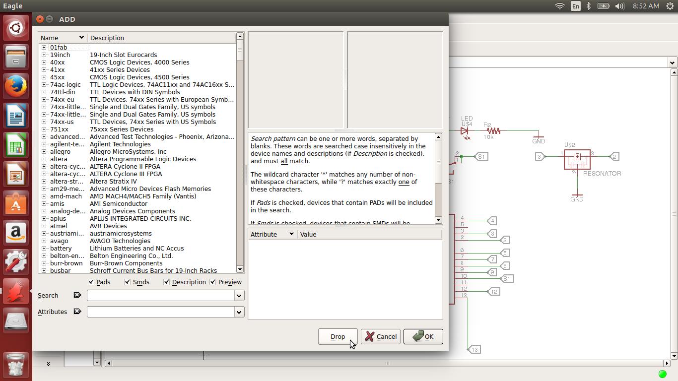
This week I have to take a pre-designed board and add something to it. So, I worked with the Hello World board and added a button and LED. I decided to use Eagle CAD, since I haven't had any experience in electronics ever. First I had to install the fab library, which went pretty well. In the Ubuntu interface, it was a matter of navigating to the folder, dragging and dropping. When I opened Eagle, I had to choose which library to use, by clicking Libraries>Use and then selecting it from the drop down list. Then I started a schematic.
I followed the tutorial , but I still had a few challenges to figure out on my own. For instance, I accidentally clicked the "Drop" button while choosing my ground connection (I figured that "drop" meant to drop the part on the schematic, but no), and that made it disappear from the library! There is no undoing that button...
What I eventually figured out is that you have to reload the library from which the piece originated. Once I reloaded the library (just selecting all of the libraries to use again), I was good to go.
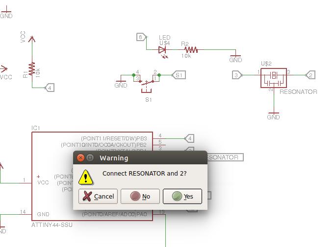
Then I made nets on all of my pins on the drawing. From there, I easily labeled the nets, and this made connections easier. When you label one net the same name as another net, a dialog box pops up asking whether or not you want these two connected. It is a good, quick way to make your connections without running wires all through your schematic.
When I thought I was ready to draw my board, I discovered some issues. I ran the ERC tool, the "Electronic Rule Check." I had about 20 errors, and most of them were related to my GND and VCC components. After much trial and error, I figured out that the net wires in all of the cases weren't actually attached to the GND and VCC components, even though they looked like they were. This was fixed by moving the components until they touched the wire in the correct place. Then I tested each connection by grabbing it and moving it around, if the wire came along for the ride, I knew they were properly connected.
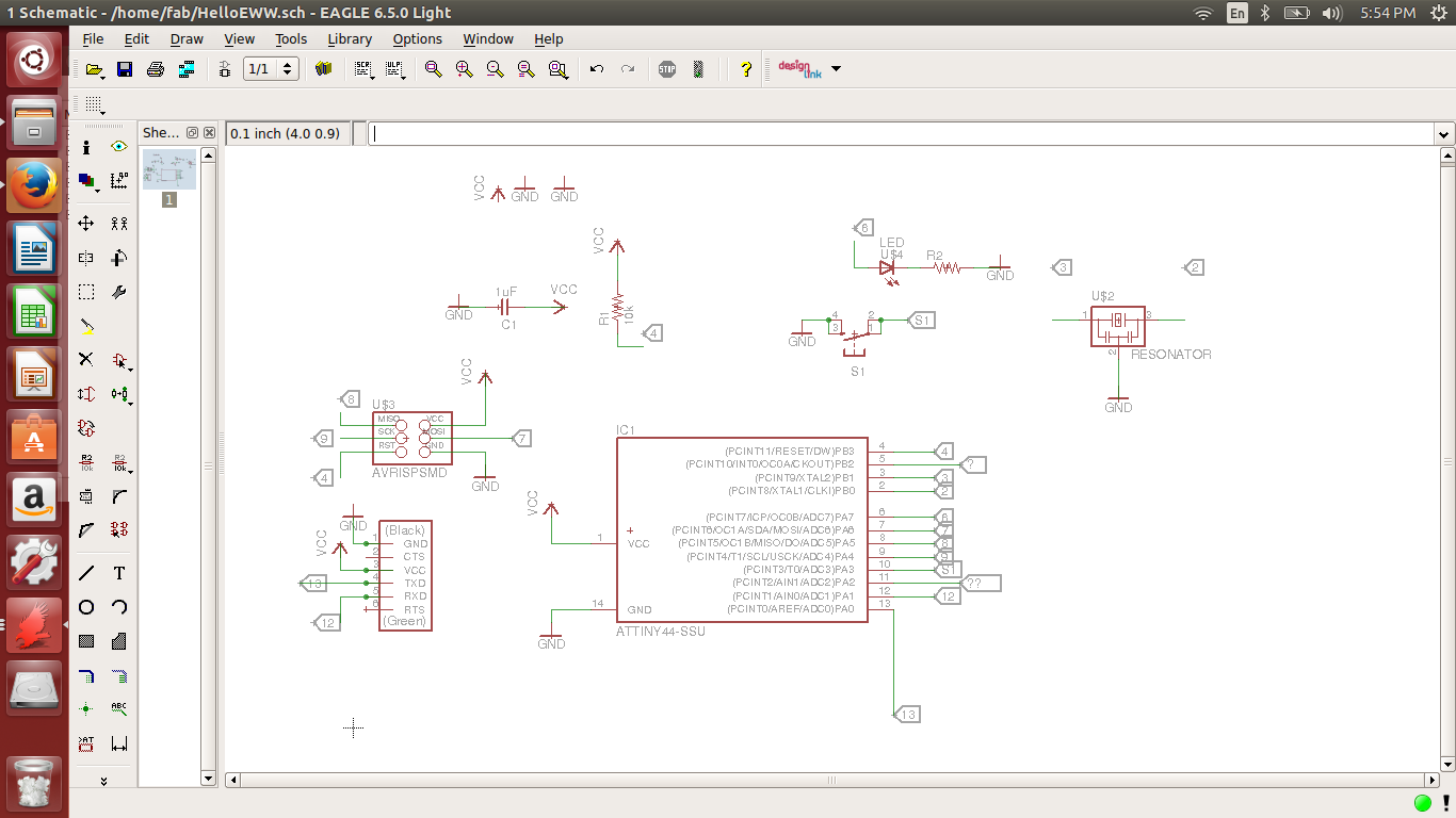
Here is my schematic for my EW Hello Board.
When no ERC errors popped up, I was ready to draw my board. I clicked on the switch to board view, and it drew my board. I dragged and dropped my components onto the big box and I messed around with their location a little, now really knowing what to look for. There were the yellow "air wires" running everywhere, so I decided to try to autoroute the board, thinking this would be the easiest way. This was the result from my autoroute experiment:
There were blue nets as well as red nets, with green circles everywhere. From experimenting with layers, turning some off and then back on again, I was able to determine that the blue lines were run underneath the PCB. This wouldn't do for my milling process, so I concluded that autoroute sucks. Then I spent a lot of time googling how to undo autoroute, which turns out to be pretty easy actually. You just type ripup; in the command bar.
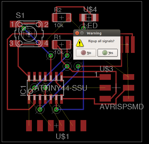
Once I ripped up all the terrible routings, I started manually routing the board, which ended up being challenging. It takes a lot of thought to figure out how to route the traces without crossing over one another. It reminds me of the Free Flow game, which I am pretty good at.
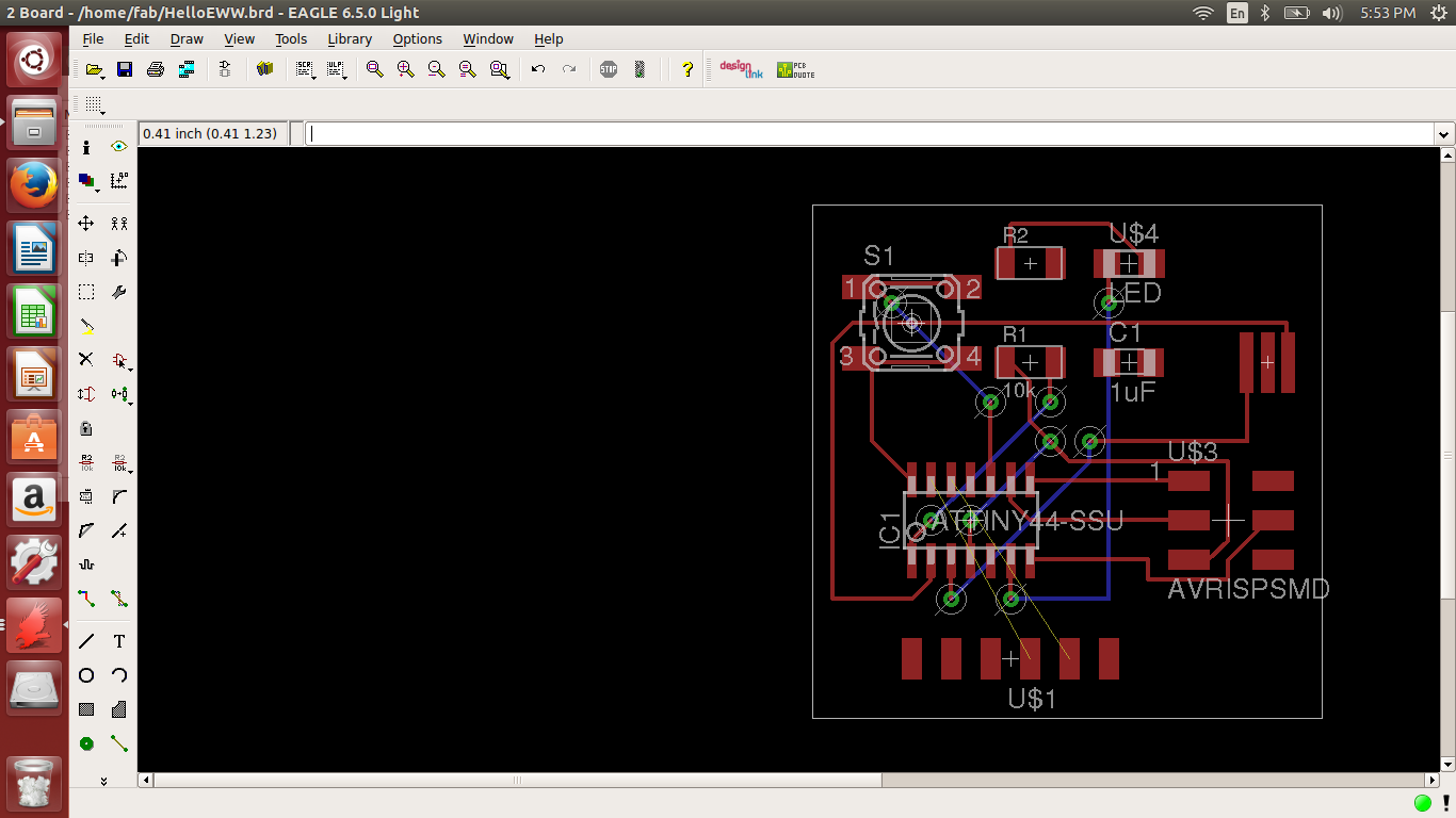
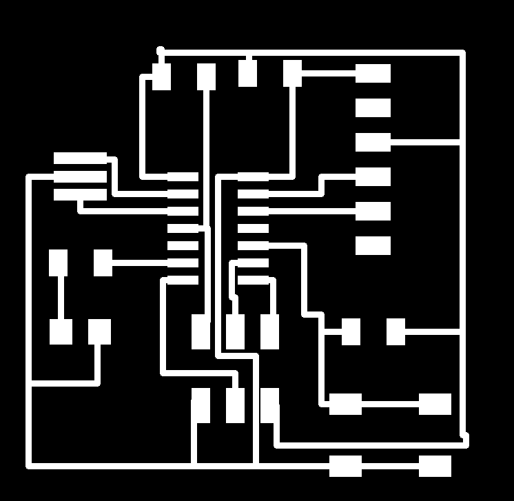
Here is my board diagram, traces complete.
I changed the design rules using the DRC button on the toolbar. I changed the clearance to 0.41mm in order for the Modela milling machine to be able to mill in between the traces properly.
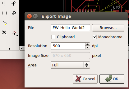
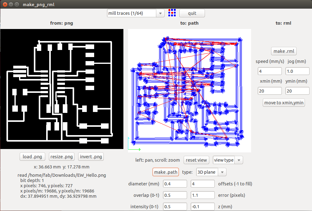
Then I cleard all the layers and just had the "top" layer (the traces). From the File menu, I chose "export>Image" then I changed the resolution to 500 dpi and checked the "monochrome" box before exporting the traces.
I did the same for the outline of the board, so that I had two different pngs when I was done, one for the traces and one for the outline of the board. Then I went to the Modela computer, and opened up Fab Modules by typing "fab" into a terminal window. On the dropdown menus, I selected: input format>image (.png) and output process>Roland MDX-20 mill (.rml) I changed the bit of the modela to a 1/64" 2 flute flat bit. I zeroed the Z axis and made the following selections on fab modules:
Then, I selected "make .rml" then "send it!" then, on the new window, "begin milling."
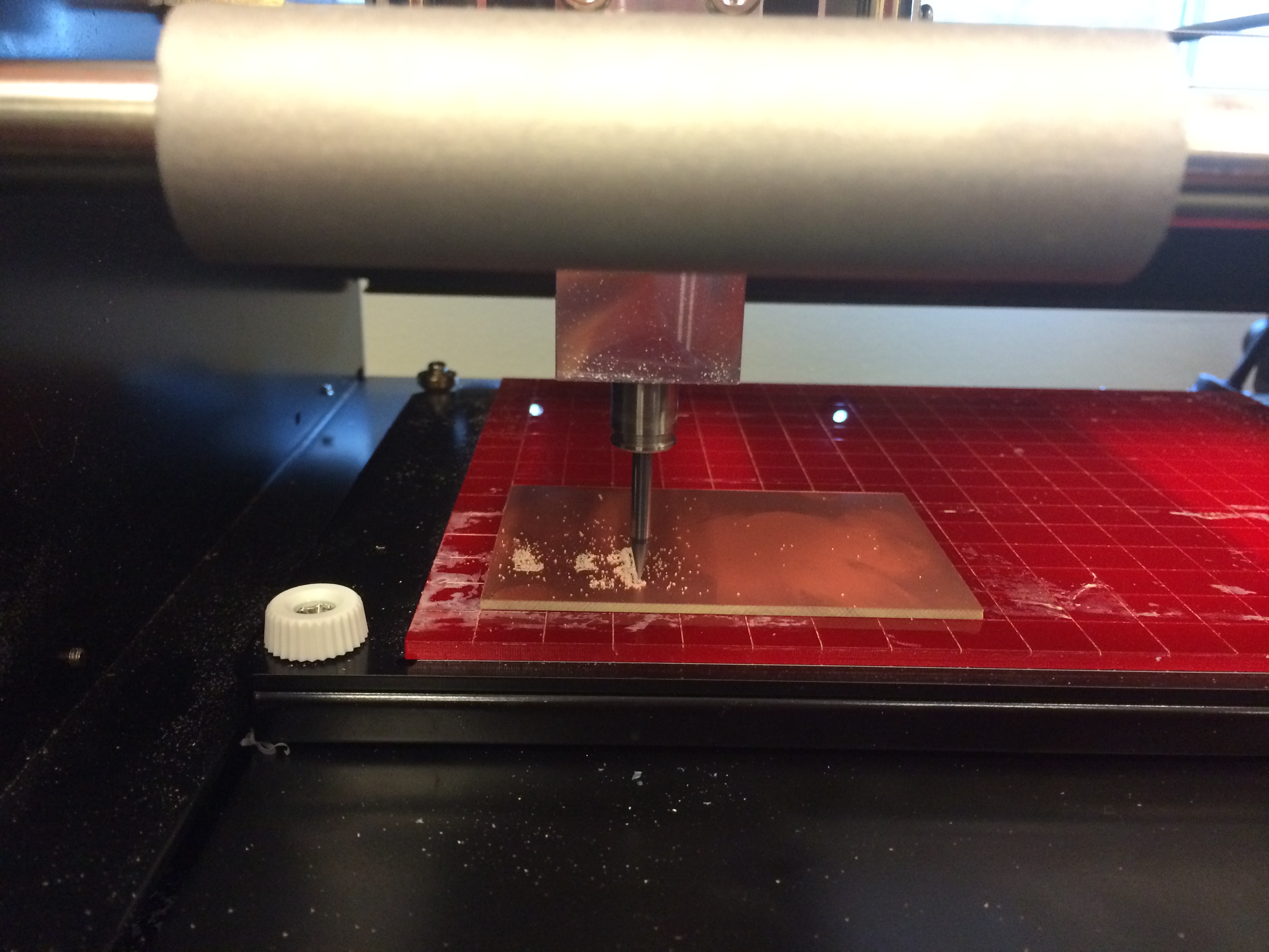
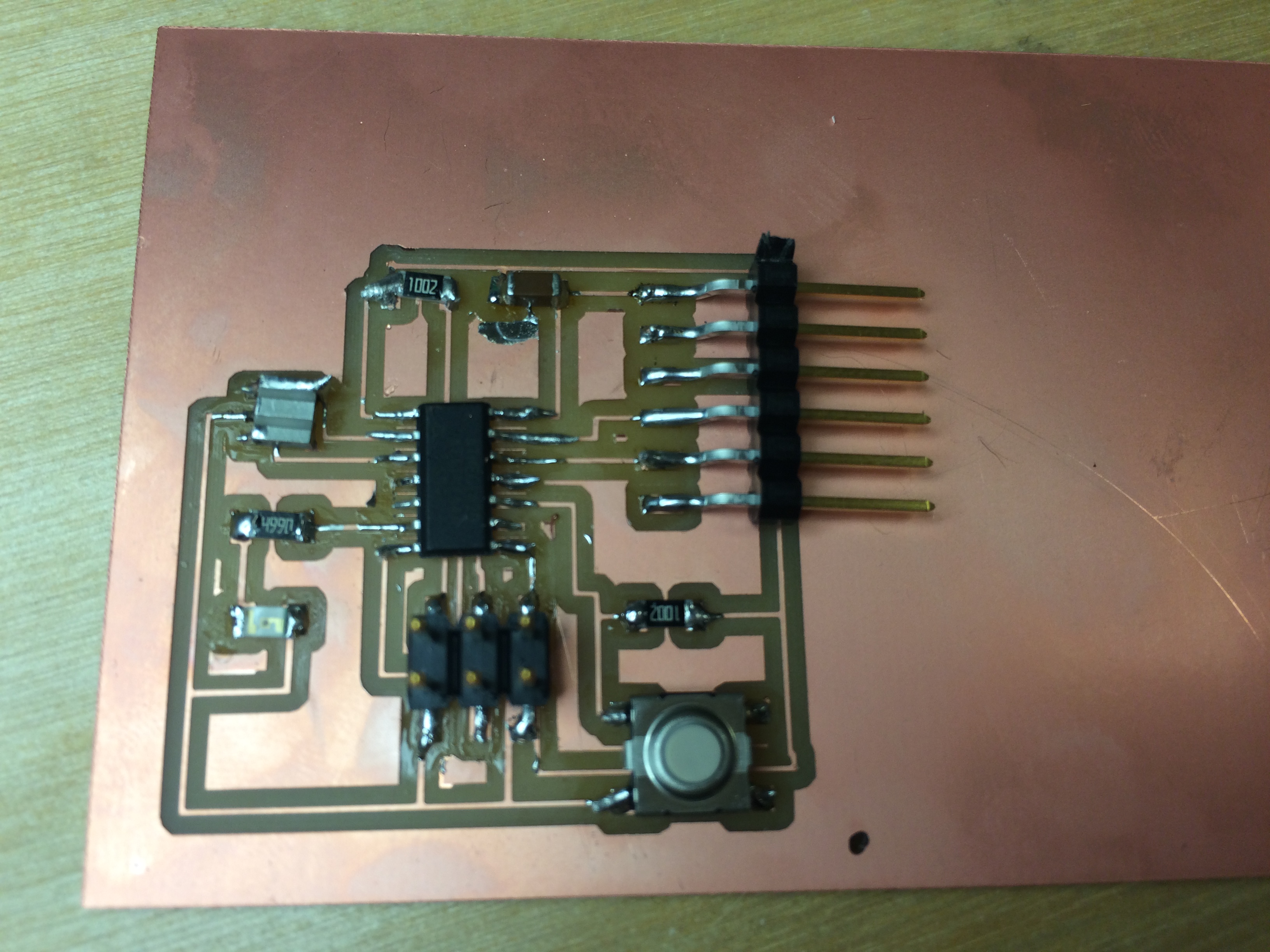
Once I had the board successfully milled, it was just a matter of finding the electronic components and stuffing the board. I'm still not that great at soldering tiny little things, so the end product was a bit messier than I would have liked.