Week 06:
Electronics Design (1/2)
Important Vocabulary
Run bom.
This is a command in Eagle that generates a parts list for a stuffed PCB.
Elia could not remember if it was rumbom or ronbum or run bun or bon rum. Since he is Italian, he rolls all the “r”s, which makes it take even longer and sound even more inappropriate as he run-boms through all the iterations. It means “run bill-of-materials," and becomes relevant later in the process ...
Objectives
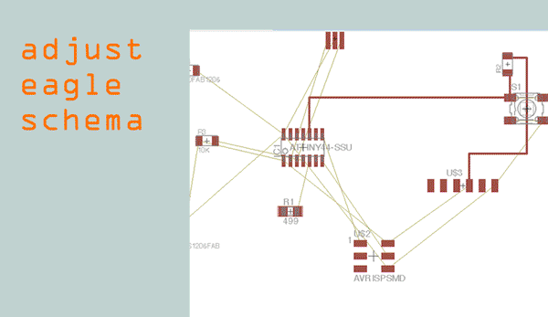
We’re modifying an existing circuit board design. The modifications are adding an LED and its necessary resistor as well as a button.
You’ll see a recap of the working process of going from learning the software to a design to a production of an actual board.
Software
- Eagle
- Fab Module for Roland SRM-20
Machines
- Roland SRM-20
Practices
Learning how to design a PCB in Eagle
** I ended up creating a more complete set of guidelines for using Eagle for Week 11.**
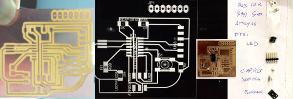
Starting from an already-created board, we sourced a few more additions and figured out their values.
Let's look at sourcing the LED.
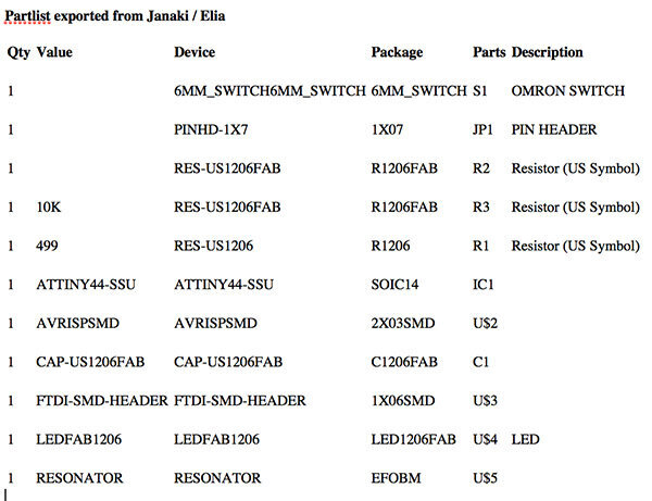
To find part numbers and specs, it’s useful to know what a FabLab usually stocks. Here’s the inventory for the labs.
Let's pick an LED from the Fab Inventory spreadsheet. The LED section shows something like this:
LEDs are diodes and so will drain a battery / explode with an unlimited power source unless there is a resistor. Use an online calculator to find resistor values for LEDs. For the LED I'll use, to deal with potential voltage fluctuations, it is recommended to go up a value, which puts the value at 499 ohms.
A standard resistor for most things we'll do is a 10K resistor, and you'll see two of them on the schematic.
Look up the part number in Digikey a to see the data sheet that shows a footpad ~ this can help determine how far apart and how large to make the pads for the component.
And a few tips for the processor, an ATTiny 44.
To determine what the pins on the chip do, see the pretty little schematic from AdaFruit. It indicates what I/O can be accepted on which pins and which pins can handle PWM for fading LEDs. You can see where ground, power, digital-only pins, and analog-digital pins are on the chip. Board details are at a great site called Pighixxx.
The whole parts list for this board:
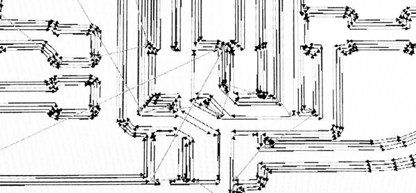
In Eagle, go from the schematic view to the board view.
Fiddling with the board design
When I did a Design Rule Check, a few errors appeared with clearances and overlaps. I had a hard time understanding why the overlaps were happening. They were actually artifacts of previous actions; when I cleared the errors panel (or turned off and turned on all layers), they didn’t reappear.
I also tried an export to PSD to make the black and white .png to export to FabModules. This was unnecessary; exporting straight from Eagle was totally fine. I exported a 600dpi .png to use in the Fab Module for milling a board on the Roland SRM-20.
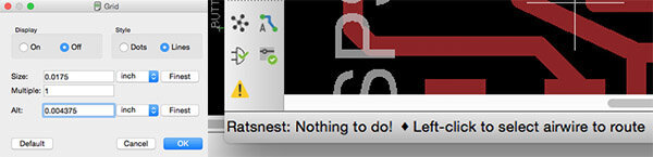
Other notes on Eagle:
The goal is to get the ratsnest to let you know "there's nothing to do." Also, it is important to finesse the grid increments so that you can move the traces with enough precision (use the alt-key for the finest increments specified).
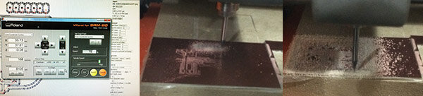
Production of the New Board
Clean MonoFab and prep the blank board with tape, checking flatness of the underlay and tightness of the tape.
Get into Fab Module.
Set for SRM-20 (the Roland MonoFab machine).
X, Y, Z to 0.
Save the file.
Open V-Panel.
Adjust x and y and hand-adjust the z.
Output to the previously saved file.
Now readjust the z and cut air to make sure it all looks ok.
Make sure all the 3-axes are set to the chosen origin, put the speed at 70%, and start the cutting. When you know all is alright, go ahead and increase to 100% (you don’t need to pause the machine to do this).
In the Fab Module, you calculate 4 offsets. When I did this, some of my components has merged with the traces. I went back to Eagle 4 times to make minor adjustments to the positioning of things till I had separated pads.
The bit was not biting enough and we readjusted the bit to be a fair amount deeper ~ about .1mm deeper. Probably a dull mill. You can see in the photo the difference between the light traces from the first attempt, then the second go-round, which is producing the right color of dust (it should be yellowish, indicating that it is cutting into the substrate below the copper).
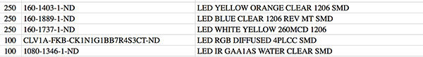
In Eagle, “run bom” to get a parts list. Then, off to solder ...
Assembling:
Completion:
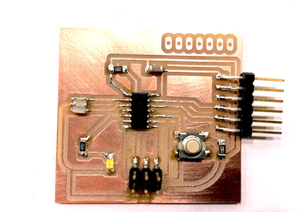
It survived testing with an ohmmeter to check for connectivity. We'll see how it does in a few weeks with some I/O!
Events & Ideas
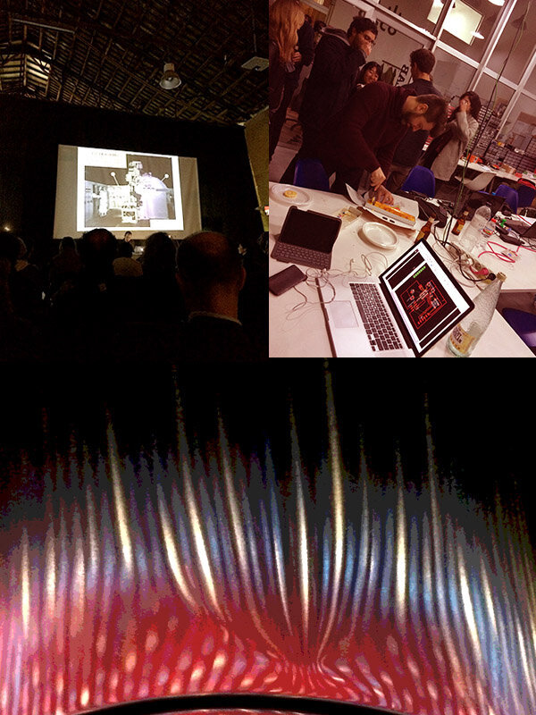
recitation: Kenny Cheung, from NASA and MIT
Some ideas from him on which I picked up:
- "picking a point so far out that the scope of the problems is really vast” ~ Kenny is talking about all the things that have been developed for consumer use through the research used for life in space
- know the bubble that exists so that you can know where you are in the bubble and position yourself at the edge of the bubble
- learnt from urbanism: we’re limited in the size of thing we can build top-down, with all its parts engineered and designed at once ~ the complexity of the thing is limited (listen up, Bernie Sanders)
- Kenny went from architecture to space. "I still think of myself as an architecture student. I think of myself as other kinds of students as well, that’s the only thing that’s changed."
IAAC winter lecture: Daniel Cardoso Llach
He was in the first class of Fab Academy students in Barcelona. He studied architecture at MIT and teaches at Carnegie Mellon. He read his lecture, and I was distracted and impatient, so I only learnt a few little things.
- CAD proposed in 1959.
- Technologies are not neutral, but propose philosophies.
- Technology as infrastructure, not as tool.
- Avoid deterministic positions on technology.
- Cool photo of 1952 machine that uses math to build construction parts.
I was immersed in electronics design with Eagle when the lights went out and the class came in singing "Happy Birthday." For me! Sweet, and we ate sweet ice cream cake.