Week 04 - Electronics Production
Assignments:
- Making a FabISP in-circuit programmer, by:
- Milling a circuit board
- Stuffing it (to solder the components on it)
- Program it
- This week’s assignment page
Milling a PCB: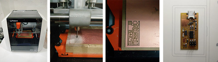
-PCB stands for Printed Circuit Board and is a good solutions for mounting/assembling/soldering our electronic components together. It keeps things organized and fixed, if you compare it with soldering a bunch of wires instead.
So the board is something solid covered with a thin sheet of copper that we etch or mill (or other process) the copper away, leaving just the path where we want to conduce electrons to our electronic components.
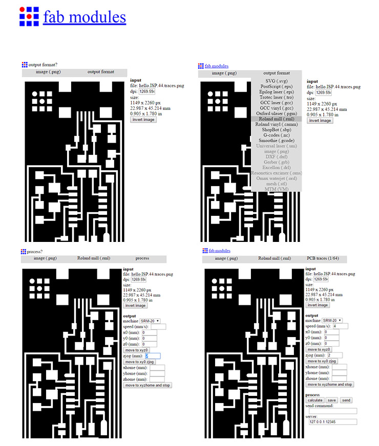
We started by our board, milling it in a Roland machine SRM-20 to create the path, and to do so, we used some already designed models of ISPs. I went with Neil's model but I still want to create my own just to practice. We had 2 PNG files from his design, one is the outline (I call it a frame) that is the cut out frame, and the other file we have are the traces which are the paths.
We used fabmodules.org to convert the PNG files into Gcodes to the Roland machine. Very useful tool I'm very glad to come to learn.
The steps I took in Fabmodules were, first load the file on "input format" selecting PNG, the "output format" select "Roland mill (.rml)". Observe on the right you have now some fields to fill. For "output" select the version of the Roland you have, in my case was the SRM-20, leave speed empty,for x0, y0 and z0 fields, fill each of them with a zero (0). This will make sure you will start exactly wherever you "zero" your X,Y, and your Z too (To Zero the machine is a process you will do on the Roland's software). Zjog is your safe distance, the distance the tip of your milling tool will be travelling from your material. It suggested 2 mm, I made it 3 cause I felt like being very safe. Leave everything else blank. Now click on "process" which is the process you want your Roland to execute.
Since I selected the traces image, now I also selected here "PCB traces (1/64)", 1/64 being the diameter of the milling tool you should use. Note this is in inches. In mm it would be around 0,4mm.
Now you notice a process field tree on the right side of your fabmodules, with Calculate, Save and Send right under it.
In cut depth you may want to go 0.1 mm, your tool diam is 0,4 as I just mentioned above. Number of offsets is how many times you will repeat the same rail, but each rail the milling bit will offset, milling the path a bit wider. How wide, it will depend on the Offset overlap(%) you set. Set 4 to number of offsets and 50 to offset overlap.
-Next step is to make sure the platform of your milling machine is clean and flat, this step is very important. A little bit of time spent here saves you loads of time later. Uneven beds will most likely break your milling-bit besides the fact it won't mill it right, and you don't want that. Dusty or greasy beds won't stick properly besides might generate uneven results by fixing your board to the platform/bed. (As you can see in the picture below, our MDF bed was very damaged. We had to mill it flat, after damaging some boards. Waste of time, and we don't like that.)
Now, at the back of your PCB (the part without copper, if you have a single sided) make sure it is clean and apply double sided tape, leaving the tip of the tape outside of the board and the end outside too. This it means you start taping before the PCB, tape it all through, paralel to the side and all along till the board ends, and cut it 2mm bigger than the end of the board, more or less. This avoids any wrinkles. Avoid bubbles too.
Now that you have your board tape-fixed against the bed of the milling machine, time to "zero" the milling machine.
Open Roland's software VPANEL, and find above "speed" the setting X and Y button and setting Z button. Before you set (also called "to zero") X and Y, bring the tool to the position you want it to start your job from. Remember, it starts from bottom left corner. Once in place, hit "X/Y set origin point".
Almost same thing with Z, just that you will bring it very close to the board but not exactly touch it (Remember, great chances you break your milling bit if you do touch the board). Now once the tip of your milling bit is very close to the board, you will manually release the bolt that holds the bit, let it now touch the board, screw it back, and now you hit "Z set origin point". (Don't ever lose this HEX tool. Not that easy to replace it)
Now it's time to load the file we generated on Fabmodules. Click on "CUT", delete all files in case you have any and load yours. Easy task. Once you hit "Output" the job will start. I particularly believe they should have a "Start" button instead of "Output". If you never used the machine before and not following any tutorial, you would wonder "where the heck is "Start", am I doing something wrong?! Well, maybe they don't want you to use the machine with no tutorials or training.
You're milling it! ... and you're done! Nice job.
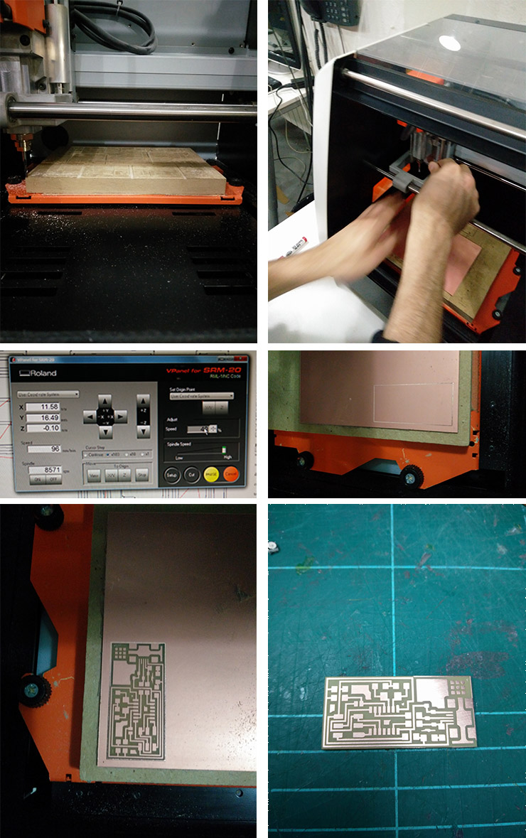
After your board is milled, clean it by rubbing it with steel wool enough to polish it a bit and then soap and water.
Once dry, let's start:
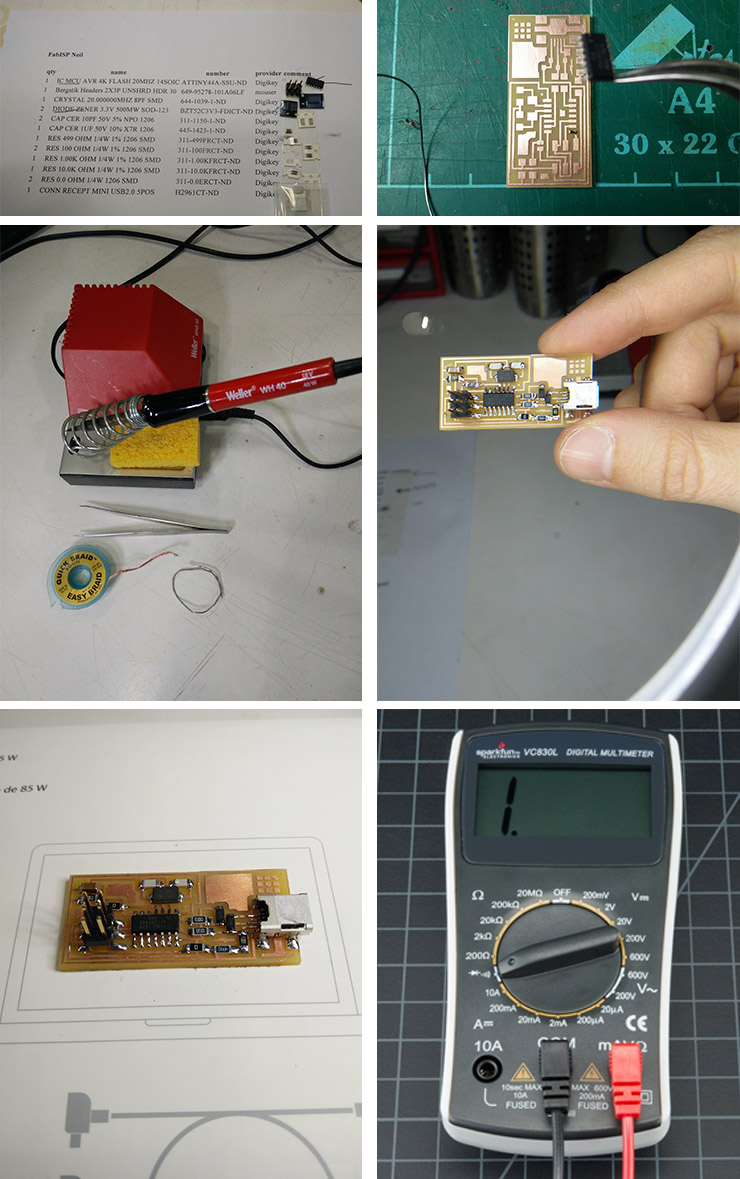
Stuffing your PCB:Ready for some soldering? Let's first find all components so once we begin we can go all the way, not wasting time standing up, looking for parts, coming back, turning on and off the soldering machine or leaving it on for too long. Remember, we like our green planet and we also do like the tip of our soldering machine NOT oxidized (This is what happens when the tip of your solder is for too long hot without solder to seal it. It oxidizes, then soldering is no fun any longer).
All componets listed and sticked to a double-face tape on the side of your list so you won't loose any littly tiny part?
The tip of your soldering-machine touches the copper plus the part of the component you want to solder. 4 or 5 seconds might do, depending on your device or tip. I had a very thin one so it took this. Now you add the soldering-wire. Be sure you have tin on the component and on the copper. Remove the wire, then remove the tip of the solder-machine. Try it first somewhere else. We had some old PCB's laying around we could practice.
HINT: Start with the microchip first then the USB adapter. Then straight to the tiny parts. Leave the Headers (The high spiky 6 legged thing) since it is the higher part, it will block you to solder some other minor parts.
Use a Multimeter to check all your soldered components with their path. This is called Continuity Testing. In the picture below, you see the right set of the Multimeter to verify the continuity.
All good? Nice! Now it's time to:
Program your ISP:Programming your programmer can be a nightmare. If you have windows 8 or newer versions of MACs, for what I heard. I have Windows 8. So it was NOT fun.
I installed WinAVR, got the firmwares but couldn't make it for windows 8 to find it.
Please if you made it, please share it! You find my email at the bottom of this page. At a level I gave up and used Arnau's macbook to program it. I advise you to read this tutorial by 2016 Fab-Academies' archives. Once programming is done, on the Mac I was able to find my Programmer in one of the USB ports as "FabISP". Happy!!
Thank you Arnau Tàsies for your help. "Bunda"! (Inside joke, don't bother)
Now:
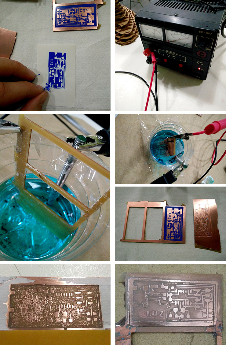
Experimenting Etching with Electrolysis: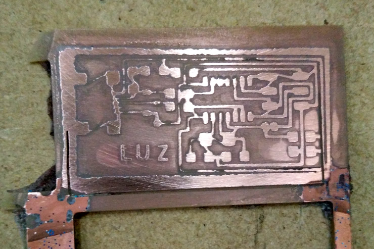
We can consider ourselves lucky to be where we are (Fal-Labs, Fab-Academy) and have access to all we do have.
But not everyone has access to a PCB milling machine.
Electrolysis is a simple process and very accessable, so if we can make it to ace this process, I see it as a very nice way to democratizing PCB Making.
Ingredients: Power-supply;
Water;
Citric Acid; (I will also try lemon to see what happens, I'll let you know.)
Vinyl Cutted sticking Mask, or Nail polisher hand-made traces, or anything to seal the path you want to remain.
Just google "Citric Acid", I bought mine in cristals, looking like kitchen salt. It's very easy to find. In supermarkets, drugstores,...
Solve the citric acid in water. 3 tea spoons in 200ml water and stir.
Important is that the Negative electrode will reduce and the Positive will oxide. From both electrodes we can profit, but now what we want is to oxide the PCB, giving away all its unprotected copper, that will be deposited on the negative electrode.
From Chemestry lessons I remember that the Cathode reduces and Anode oxidizes. So the Copper PCB is the Anode, and for Cathode I used a screwing steel rod (first thing I found that would be OK to use as Cathode).
I set my power-supply for 13.5 volts. The higher the faster, but lower also works. I've seen people doing it with less voltage.
It's nice to remind you that if you invert this, setting the PCB as the Negative electrode (Cathode now) and for Anode you use Tin, well, you are now coating your PCB with Tin. It works, I tested. But How good this is, I want to hear from you cause I didn't try soldering on it yet.
My results were not satisfatory for the small traces we have in this project, so I'll design a bigger version and try again. Would be nice to produce a programmer like that.
More pictures on Flickr:

-Download my files:
-Files week04 on Dropbox
Back to top