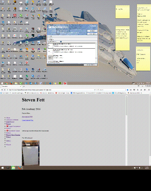
Steven Fett
Fab Academy 2016
3D SCANNING AND PRINTING
Electronics Design
3D SCANNING AND PRINTING
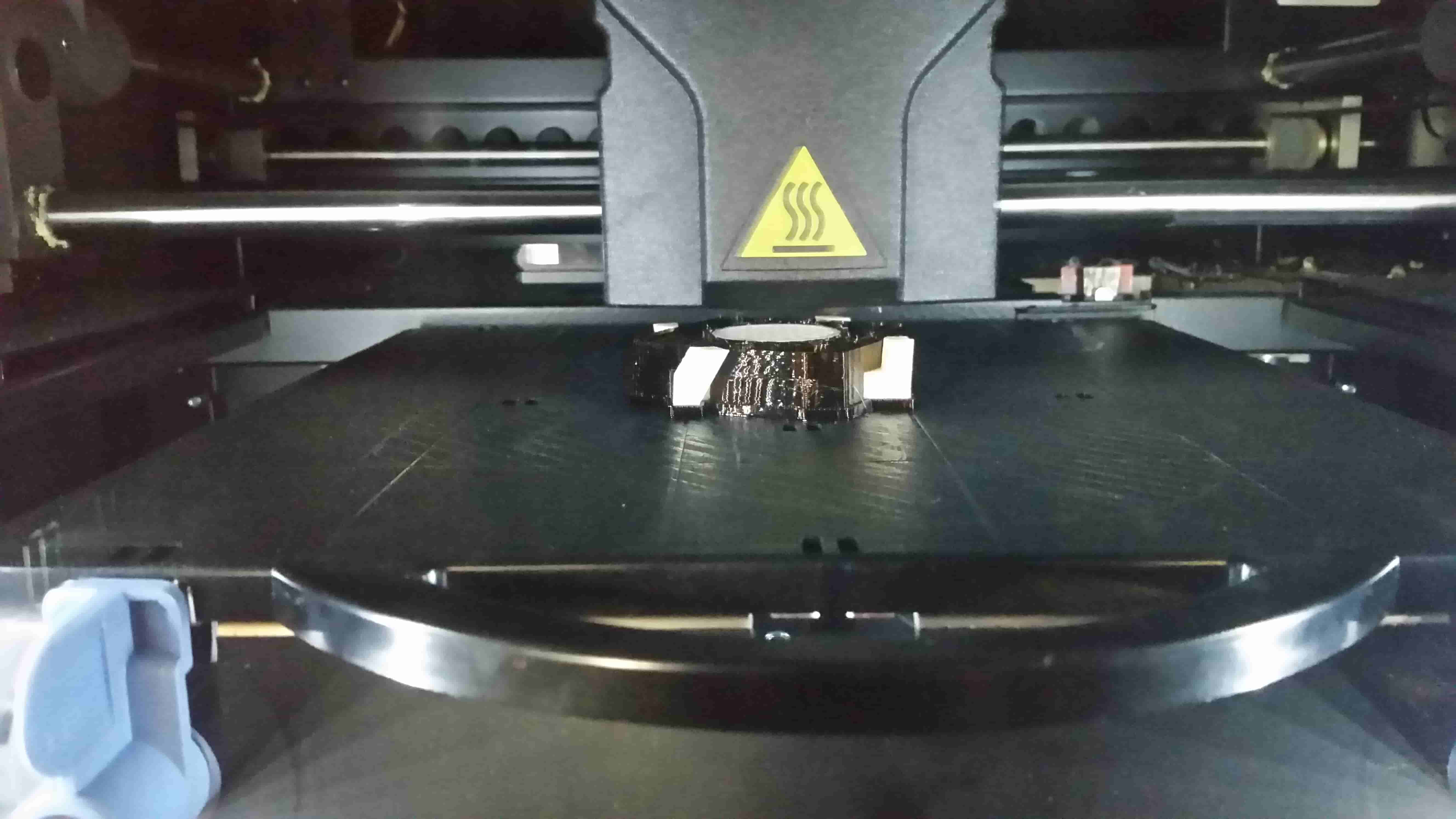
I'll be trying a couple of things this week. I'll try to print a mock-up of my final project, and a scanned object that can not be easily made from subtractive methods.
Creating an object that cannot be easily made through subtractive methods.
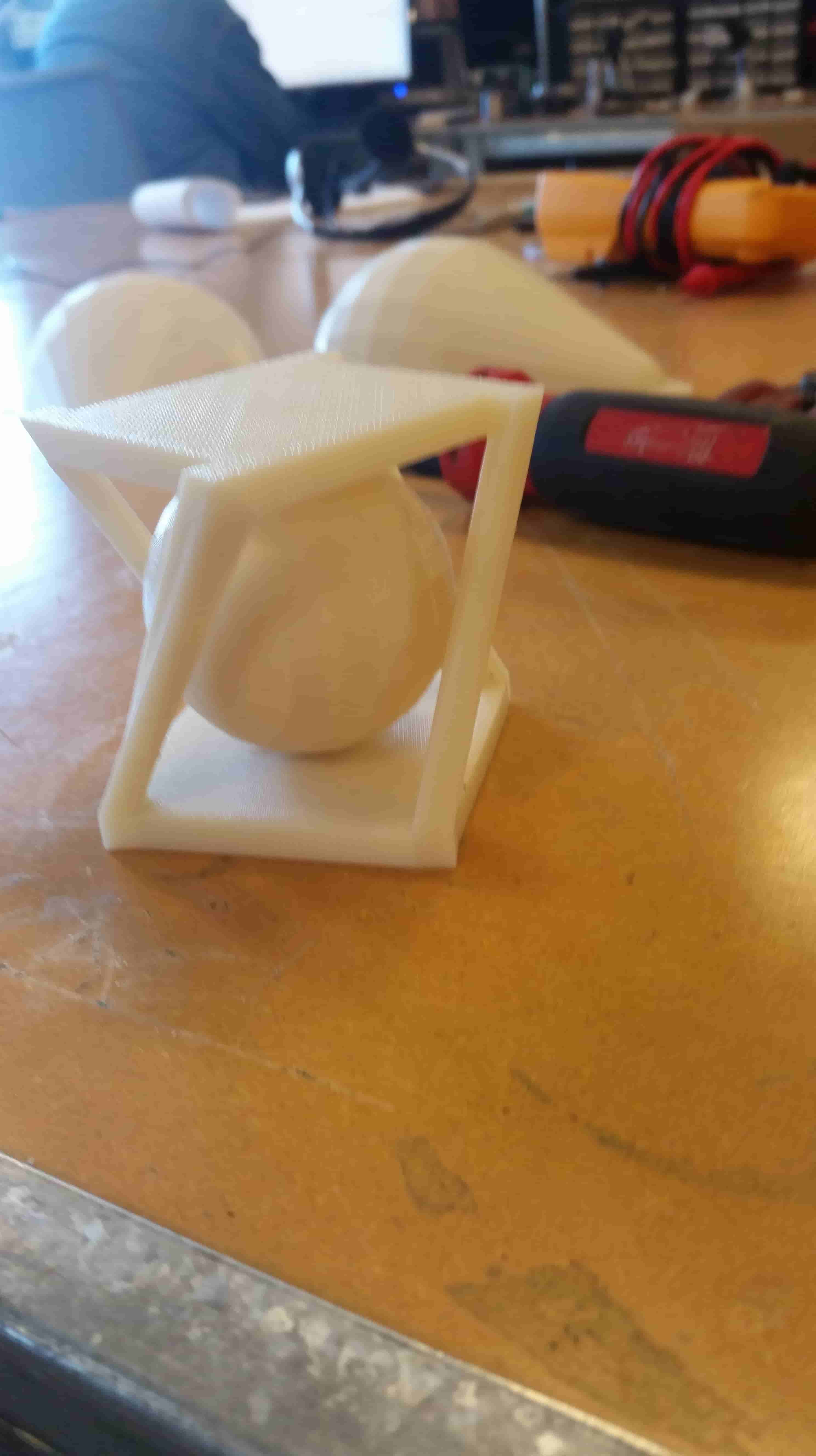
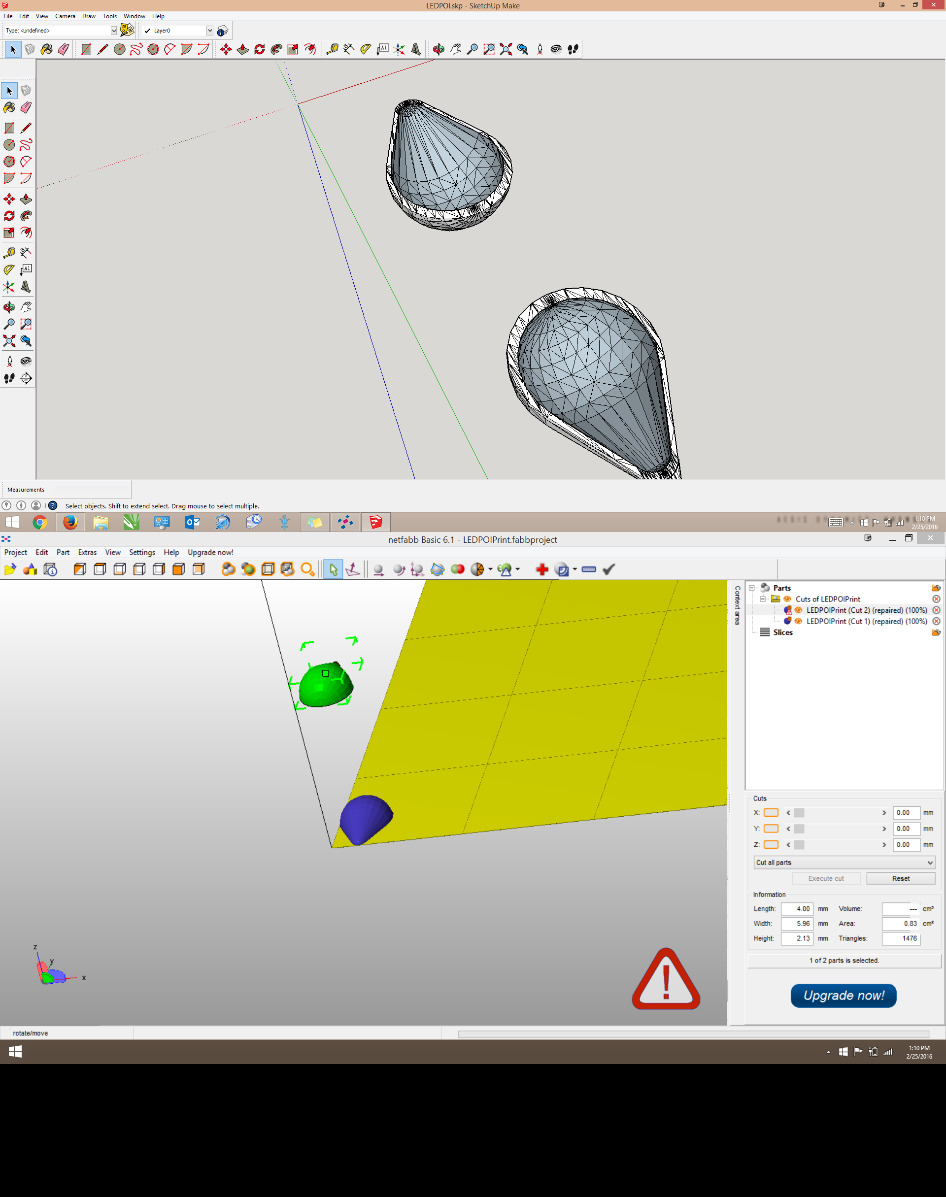
Using Sketch up I built a Captive Sphere.
File can be downloaded Here
Bonus: Gif of how I made the last gif
( project files for these gifs are located here )
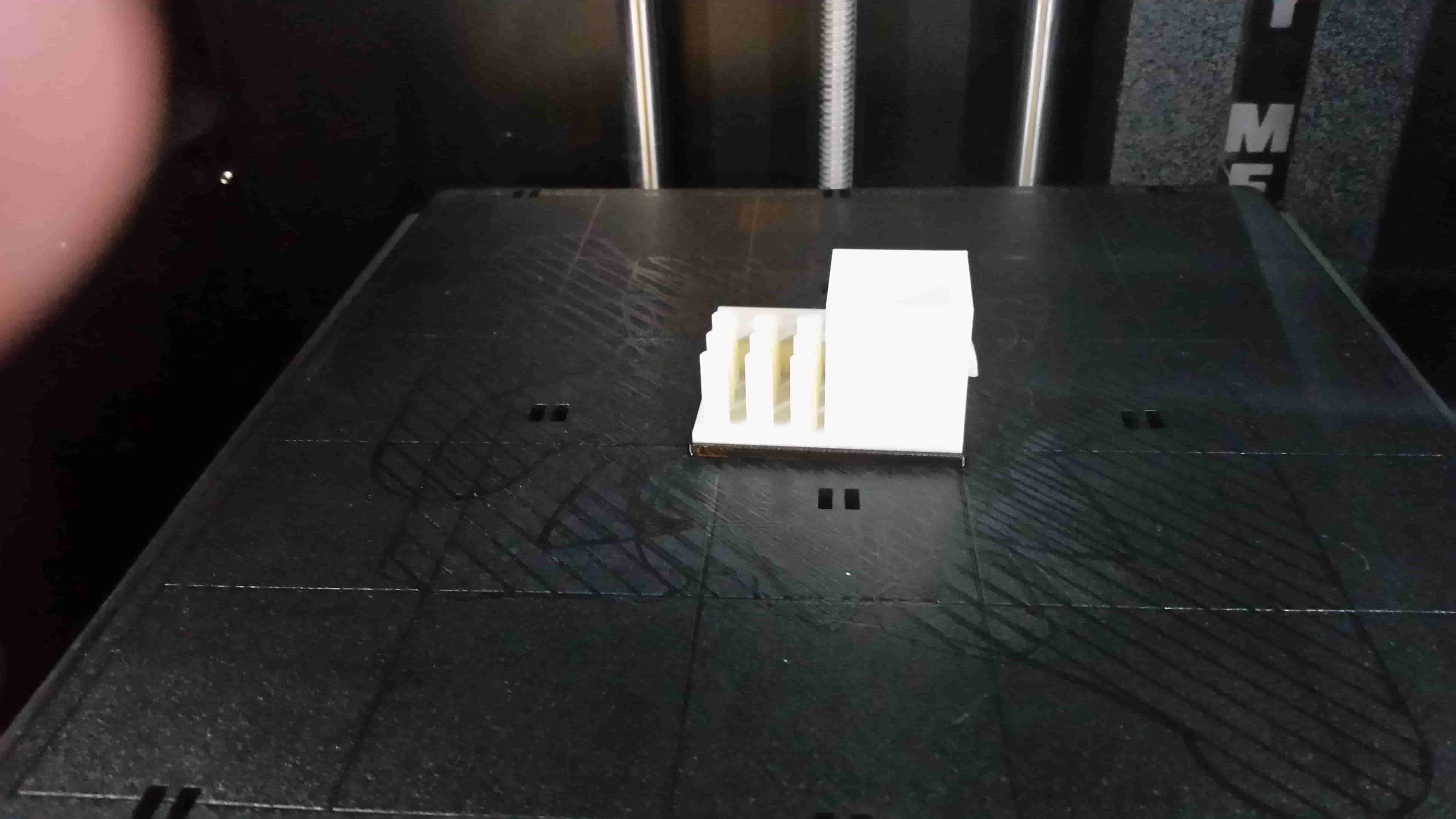
At this time my Captive Sphere is still printing. (3/1/16 14:55 AKST)
Update: It Lives!
3D Printer Torture Test
We ran the Make(TM) Torture Test on our Dimension and MakerGear 3D Printers.
Dimension 1200ES
Maker Gear M2
Update:
Dimension Settings:
Layer Resolution: .2540
Model Interior: Sparse - Low Density
Support Fill: Sparse
MK2 Settings:
Skirt: On
Resolution: .23
Infill : %15
Shells: 2
Tool 1: 215°C
Bed : 60°C
Print Speed: 40mm/sec
Travel : 80mm/sec
The results showed that the Dimension although expensive almost never fails. There is also very little control over the Dimension's print settings. Infill has 3 options, and support is ALWAYS ON.
The Maker Gear has some bed leveling issues and possible filament consistency issues. The bed leveling might be solved by having the bed fit better in its magnetic (not magnetic) cradle. I believe one issue may be that the PCB that mechanically interfaces with the magnetic cradle may have poor thermal expansion properties. I will consider having the mounting interface use the glass instead. The cradle is four 3d printed components. Since the bed is oversized slightly I may extend these clips to interact with the glass instead and fasten the heated board to the glass with binder (bulldog) clips. Inconsistent resolution on the z axis shows possible extrusion rate issues. These days simply updating the firmware of a printer can remarkably remove many issues with these DIY consumer printers.
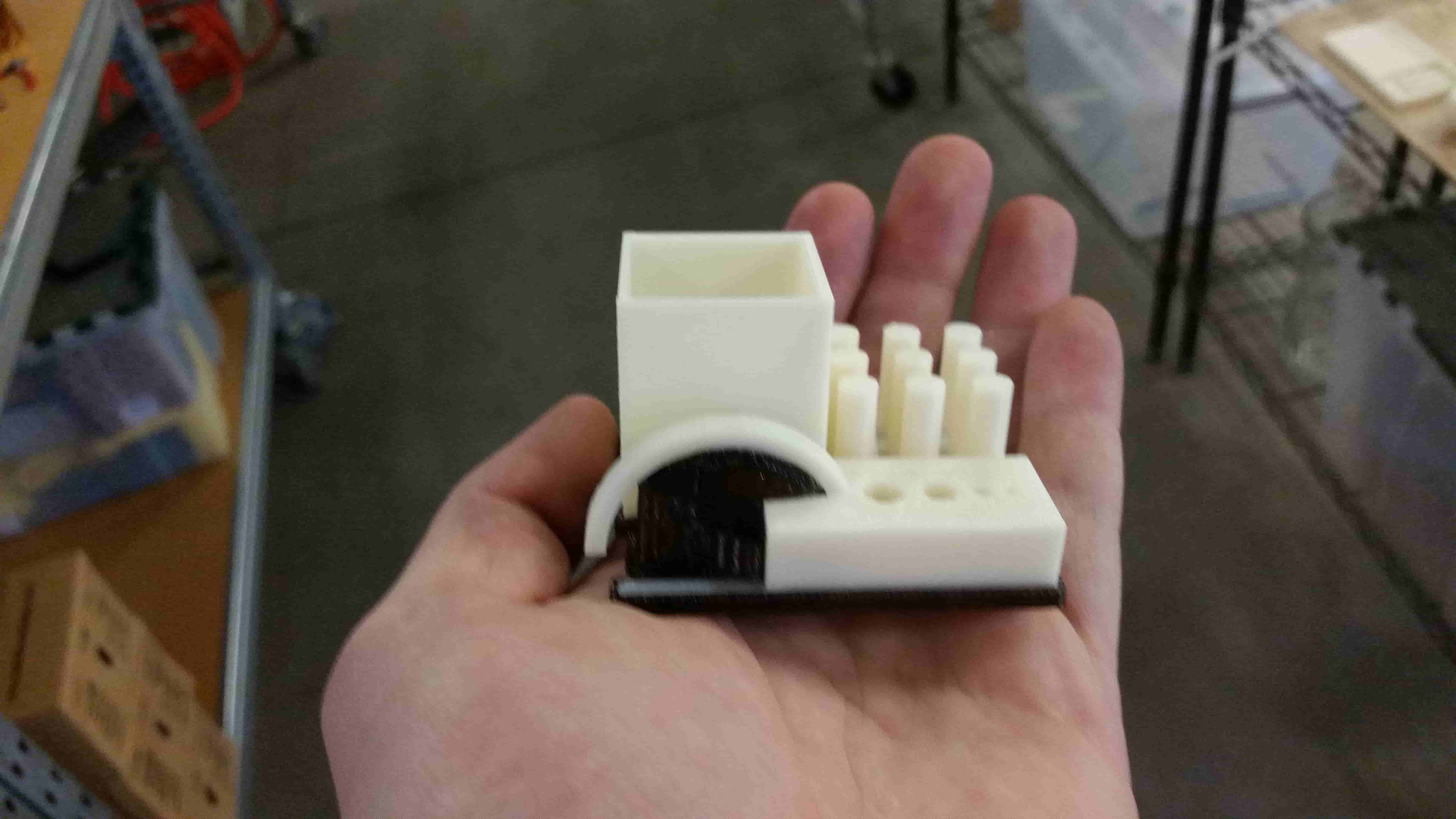
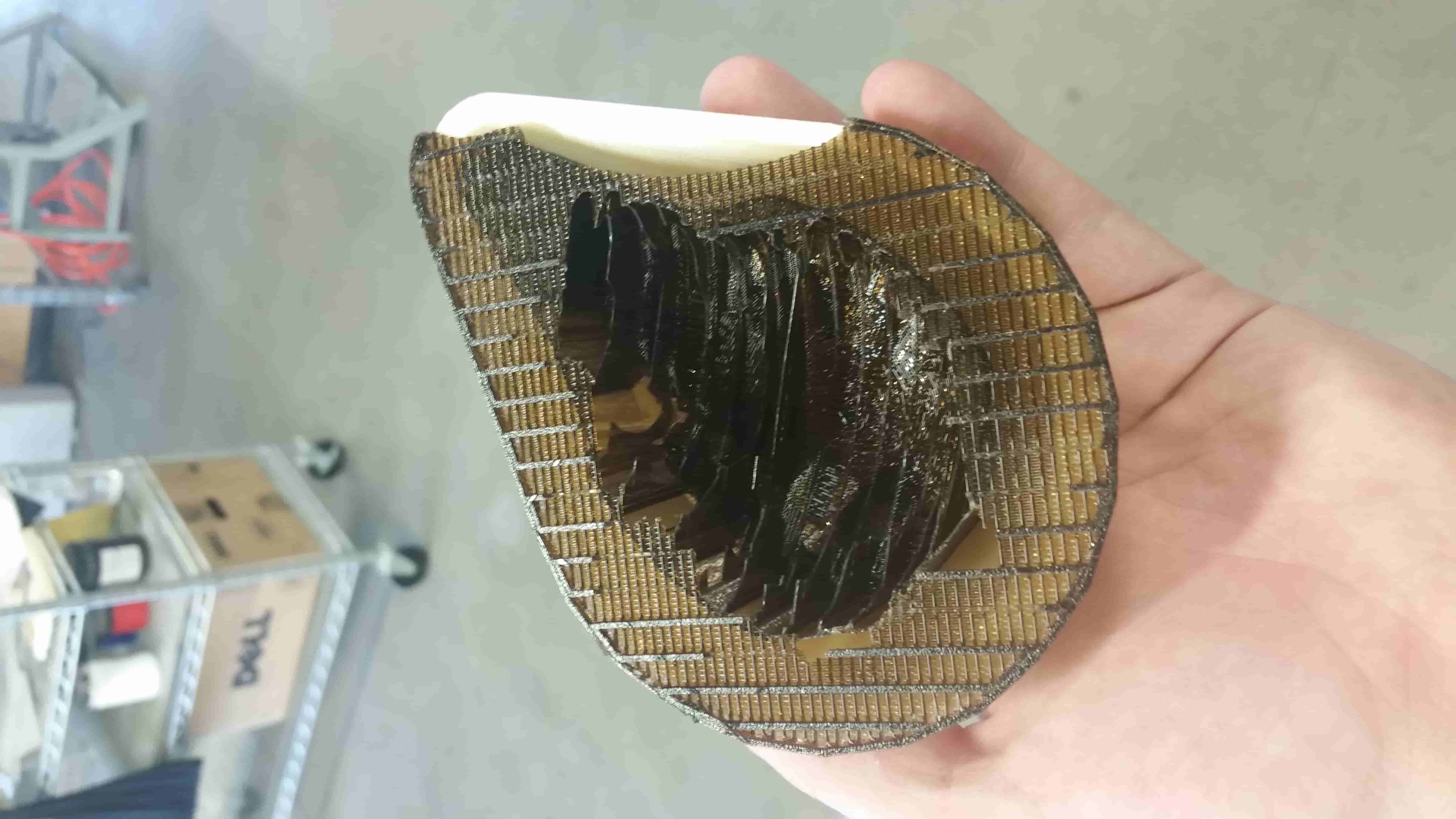
Due to what looks like poor adhesion to the print bed on the MK2 a portion of the arc could not find purchase. This left a scrambly ball of melted plastic. This ball eventually managed to find itself part of the foundation of the arc. I found the pockets (holes) to be irregular in shape and of inconsistent size in comparison to the Dimension.
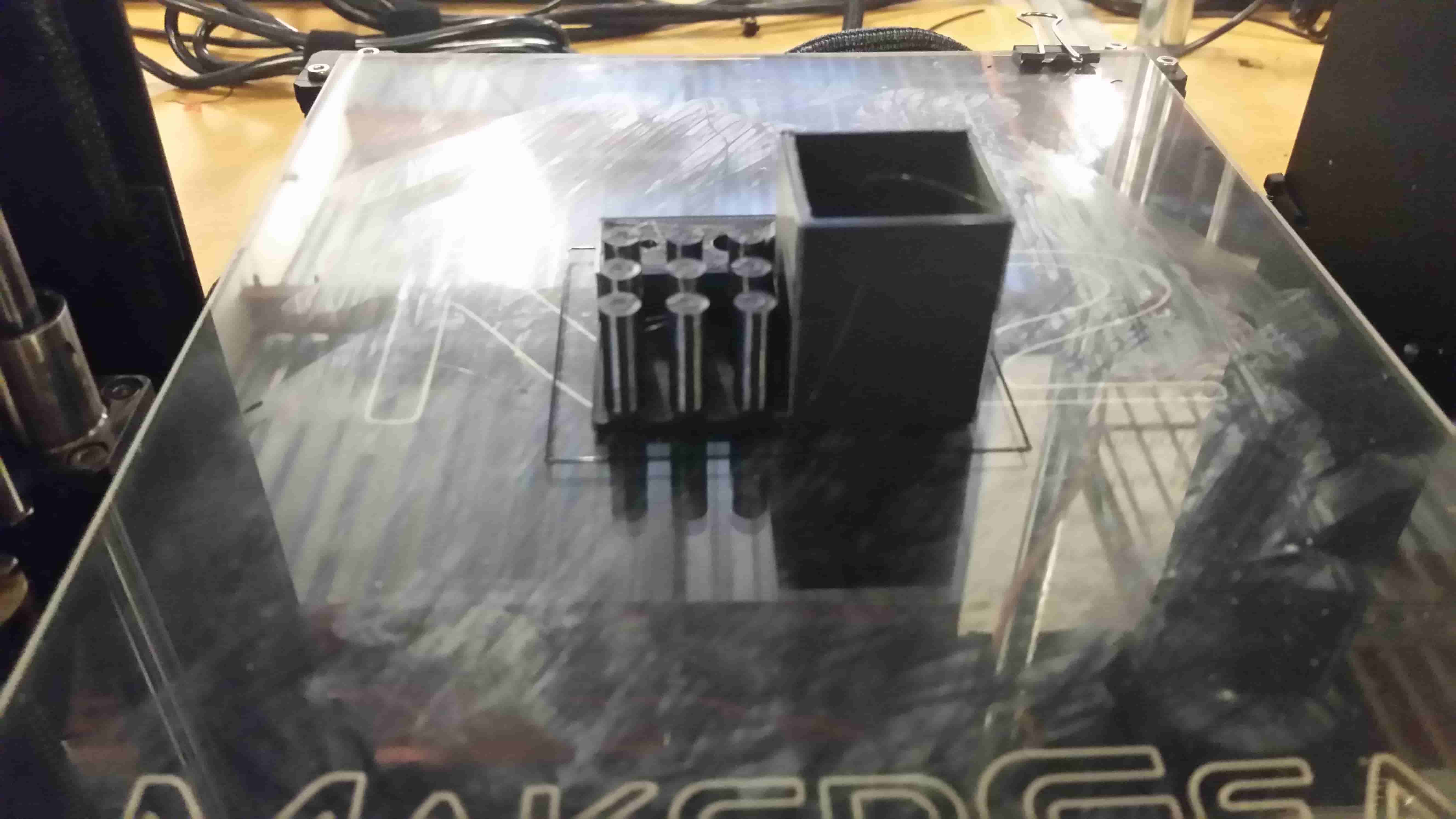
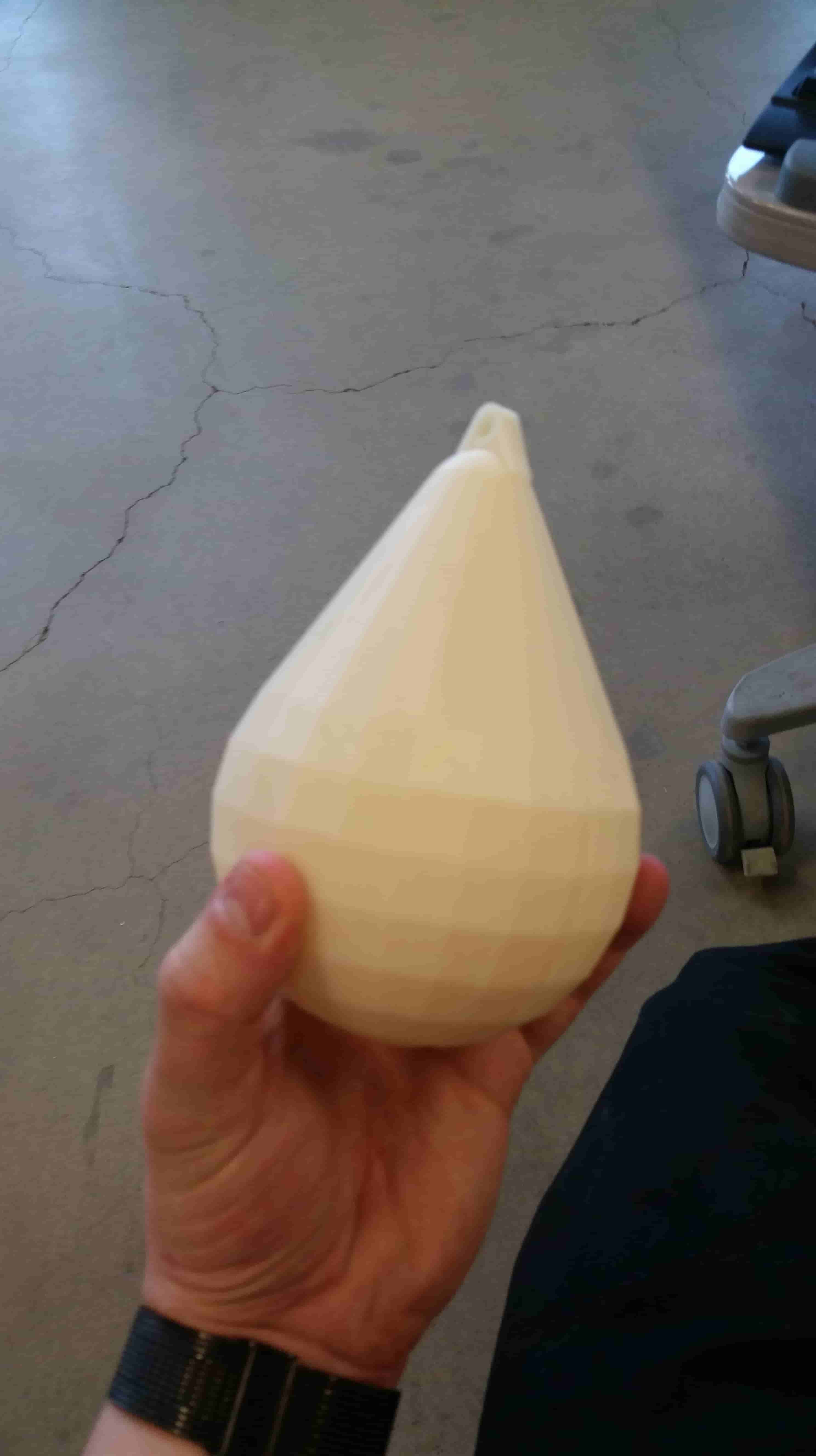
I printed a portion of my Final Project on the Dimension
Files Located here
After printing on the Dimension the parts typically need to be left in a solution to dissolve the support structure.
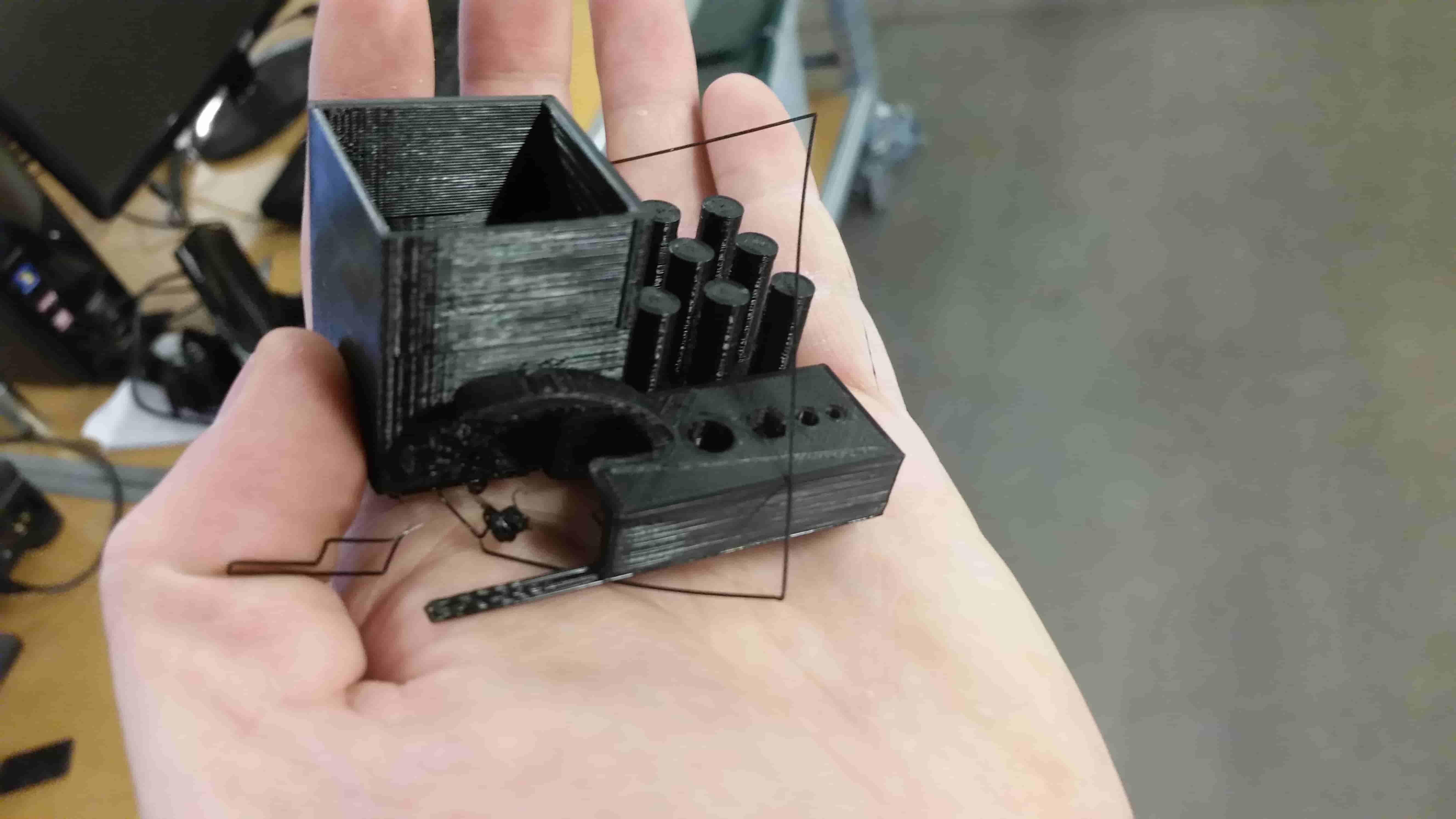
In order to allow the solution (which isn't cheap) to go a bit further I smash out as much support material as possible.
After leaving the parts in solution over night its time for a test fit.
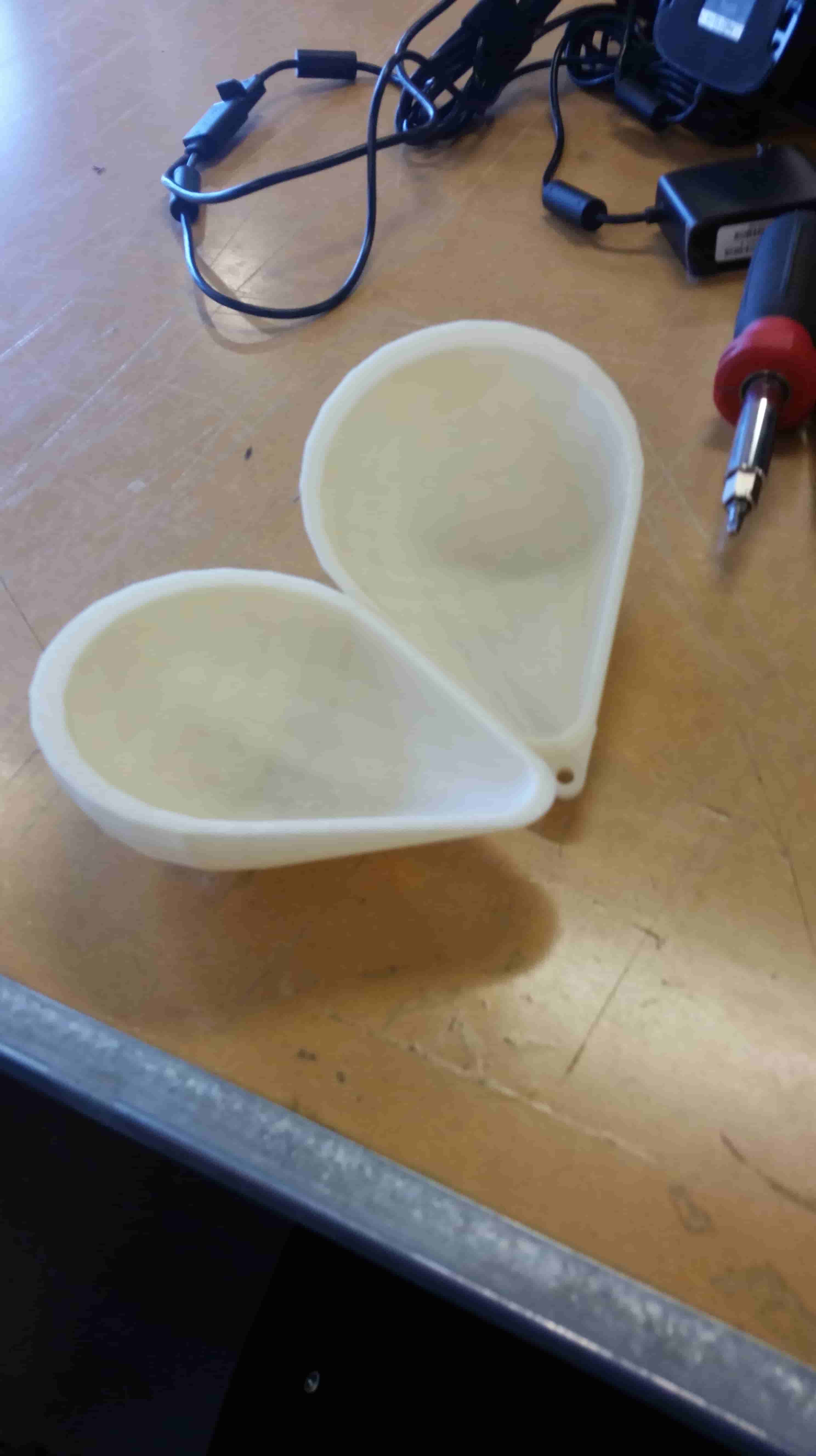
Looking pretty good.
Week 6
Electronics Design
Redraw the echo hello-world board and add at least a button and LED with current-limiting resistor or design your own
Select and use software for circuit board design
Demonstrate work-flows used in circuit board design
I spent quite a few hours on class day trying to track down the libraries and resources needed for week6. Having still not completely understood the scope and function of the project I found the lack of summary quite frustrating. I had begun to duplicate another students project in EAGLE Step by step. Yet found myself on a path that had diverged from any other design I was seeing on the FabAcademy Site.
I switched over to observing David Mason's page. I found his documentation clearer than some others.
Having spent an angry evening with EAGLE I knew my only option was to begin anew.
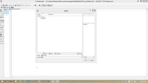
Taking nothing with me from my previous adventure except the knowledge of the software. Just for good measure I'll try building my board using different references.
I ended up drawing my sketch from the ground up.
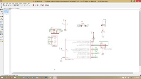
After populating my board and drawing my nets, then naming them I adjusted my component orientation.
Naming NETS is a paramount part of EAGLE without naming the NETS; the NETS will not connect to anything.
I was left with 3 orphaned traces that were not easily drawn between their components. I added three 0 ohm resistors to my sketch and manually moved them into place on my board drawing. I physically drew the traces from my orphaned components to these resistors allowing me to jump over existing traces. EAGLE did not see that these traces closed the circuits, still showing me the yellow lines that normally mean there is an open portion of the circuit.
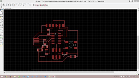
I had trouble exporting my board image. All my outputs would be images of EVERYTHING. This included component outlines and component names. I used this script I found here
http://www.instructables.com/id/Automating-Eagle-export-and-preparing-for-printing/
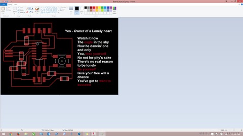
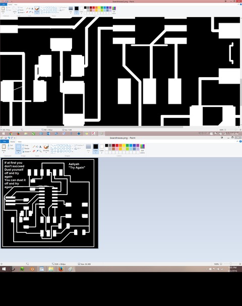
This simplified my displayed output. The image EAGLE gave me was closer, but still not ready to be milled. I took the image into paint and erased lines from the image I knew I didn't’t want milled. Also threw a bit of inspirational text on the board.
"
DISPLAY ALL
RATSNEST
DISPLAY None
DISPLAY Bottom Pads Vias
EXPORT IMAGE C:\Users\Steven\Documents\eagle\Week62ndTryMONOCHROME 600;
DISPLAY Top Unrouted Dimension tPlace bPlace
"
Milling the Board. While setting up for milling I noticed my traces were not defined enough for the interpreter. So It's time to jump back into EAGLE and move stuff around. I moved some of the traces apart hopefully giving myself more definition. I ran into an issue where the Fab Module lost scale and tried to mill my board at something like %200 in size. I couldn't find a way to get EAGLE to tell me the physical size of my board, I decided to measure a resistor, which sit at about 2mm. I measured the size of my solder pads by pixel count and figured out my board needed to be ~40mm wide. Inside the fabmodule for milling on the Modella after loading the desired png for milling there is an option to resize png. this allowed me to scale the image to a physical size in mm.
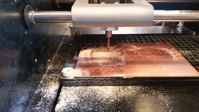
After running the board and checking the size I realized there was no way I was going to be able to load the board back into the machine to cut the circuits out of the drop. I simply ran over to our scroll saw and trimmed the board down, then filed the edges.
Stuffing the Board, this part was pretty straight forward. I called on my experience from week 4. Use a liberal amount of solder paste on each of the pads. With a razor blade clear the areas in between the traces. Referencing my board layout in EAGLE I placed my components on my board. Set the Re flow gun to 270 °C and began moving the reflow gun over the components in a sweeping motion. The components slipped around in their liquid metal pools and slid into their homes. Taking the Continuity function of the Fluke-Meter to my board, I saw no shorts, and no open circuits. I suppose the board is as complete as it can be without writing code to it.
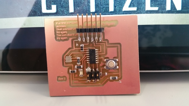
My project Files can be found here.
Archive can be opened with winrar
Update:Correct Z Zero
I was let onto another way to home the Z axis of the modela. I was originally thought to bring the bit down till it was just on the surface of the Cutting material, then run the job.
The CORRECT way I learned is to bring the bit to just above the surface of the PCB, Loosen the chuck of the Mill and drop the bit onto the surface of the PCB and tighten the chuck again.
Using the Move command it is now possible to check if the PCB is level to the cutting head.