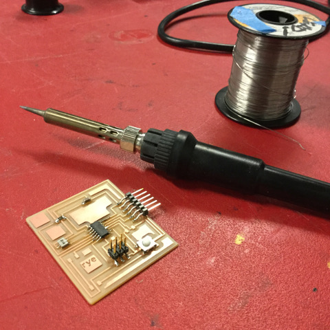
The work flow this week has been pretty eye opening. Although we had already used the milling machine to create traces and pads on a circuit board before cutting it out, we took things a step further this week. Using Eagle, a circuit board design software, we each set out on the task of creating a PCB that could be programmed to use a switch to flash an LED.
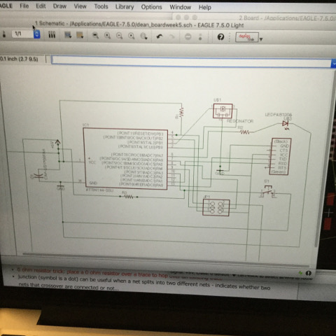
Eagle works in two related parts, a schematic and a board. I worked with the schematic first, as it is the plan needed for making a board. To create a schematic, I first downloaded a library of parts that I would be utilizing to make the PCB board, including resistors to reduce the current that would flow to parts of the board, a crystal to keep time as the board functions, a microcontroller, and a header that would be used to connect the board to the computer. As I laid out the parts on the schematic, traces, the paths connecting different parts of the board, got crossed and the web of lines got a bit confusing to look at. Since the schematic isn't an accurate visual representation of what the board will look like when created, this was okay. Traces could cross, so long as they did not come together in a junction, which would connect them in the the board representation in Eagle. After working in the schematic for a while, and believing I had completed the schematic, I began to work on the traces in the board layout. After using the ERC function, which alerts the maker to potential errors in the schematic, I learned that I had a good deal to fix. It is not always clear in the schematic that traces are shorted. I also had an instance where a trace ran through a resistor, instead of being separated by it. I found this ERC function very handy and was able to correct my errors as a result of using it. This time of correcting errors also allowed me to fine tune my use of the program. My colleague, Siron, showed me how to use the name and label functions of the program to create a neater and more efficient schematic.
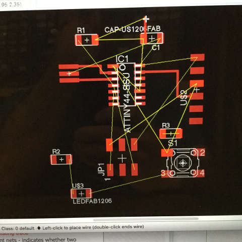
Next, I needed to begin working on the board in Eagle. After making the schematic, the parts needed were laid out on the board but left unconnected by traces. Yellow lines connected the pieces that would need to be connected on the same circuit so that no matter how you arranged the pieces, it was evident which ones needed to be connected. This allowed me to lay the components out in a more efficient way. It proved difficult, however, to create all of the traces needed to connect the proper components, since none could overlap with others that would result in a short. My first handful of attempts each ended in a dead end, with one trace left stranded and unable to be connected to its proper union. Shawn, my local instructor, finally suggested bringing the trace close enough to its destination and then jumping a trace with a zero ohm resistor. This would have been a viable solution and caused me to think about alternative methods of creating the proper circuits. In the end, I took an unconventional route to my solution. I realized that not all of the pads beneath the microcontroller were connected to something else, and so I deduced that they did not serve a function. I took a risk in using an unconnected pad below the microcontroller as a connection of the final trace that would have been otherwise stranded. I did not know if this would be a viable option, but the more that I work on these weekly projects, the more I realize that these errors are all learning experiences. In the end, Shawn told me that using the pad below the microcontroller to connect the traces was a clever solution to the problem; my attempts actually milling the board, however, confirmed my philosophy that my errors were opportunities to learn more and fine tune my skills.
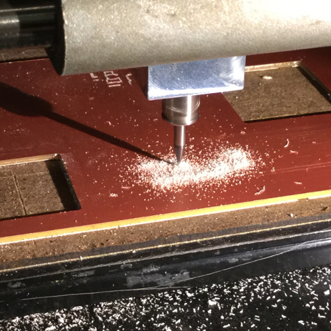
In order to have the milling machine cut the traces designed in Eagle, I needed to first convert the file into a PNG and adjust the colors to black and white. For this, I used Gimp, a simple open source image editor. After converting the board to a black and white image, I also typed my name into the image so as to customize the PCB. Once this was completed, I then created an image file for the milling machine to follow, so that it could cut out my board. For this, I simply created a box around the traces and made it black. This way, the bit would follow that design, but simply on a different setting and using a bigger bit. These two images were saved as two separate PNG files.
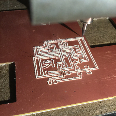
The first attempt at cutting the board was a bit clumsy. It resulted in the traces being cut out of the board, as I accidentally used the wrong default settings. It was interesting to see and I wondered if it was salvageable. In the end, I decided that it would be a better decision to use a board that was not so flimsy, as I wanted one that would last a longer time. My second attempt at milling the traces onto the board went flawlessly. When I attempted the second pass, however, in which the board would be cut out, the board came loose. The tape had not adhered the board strongly enough to the spoiler board below and it came loose, allowing the end mill to rip through a trace. In my final attempt, I ran the file again, and accidentally broke a bit by zeroing the Z-axis incorrectly after changing the big from a 1/64th to a 1/32nd bit. After learning from my mistake, I properly zeroed the Z-axis and finally cut the board out.
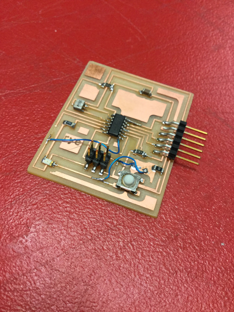
I am glad to have had plenty of practice soldering my other boards. This one seemed to go much more easily. I had thought that I accidentally damaged one of my traces with the soldering iron, and so I attempted to patch it up with solder. In reality, I had a few other mix-ups with the labels on the ATtiny in the schematic and needed to find other solutions. Having already milled the traces and soldered the pieces on there, I used a more hands on technique and made connections using some blue wires and cut traces with a utility knife when necessary. It does not look professional, but it was a learning experience, and in the end, I now have a physical reminder not to mix up the labels on the schematic with the microprocessor's layout.
Files for Electronics Design
Traces Board Schematic